Acceptor and compensating donor doping of single crystalline SnO(001) films grown by molecular beam epitaxy and its perspectives for optoelectronics and gas-sensing
Abstract
(La and Ga)-doped tin monoxide (stannous oxide, tin (II) oxide, SnO) thin films were grown by plasma-assisted and suboxide molecular beam epitaxy with dopant concentrations ranging from cm-3 to cm-3. In this concentration range, the incorporation of Ga into SnO was limited by the formation of secondary phases observed at cm-3 Ga, while the incorporation of La showed a lower solubility limit. Transport measurements on the doped samples reveal that Ga acts as an acceptor and La as a compensating donor. While Ga doping led to an increase of the hole concentration from cm cm-3 for unintentionally (UID) SnO up to cm-3, La-concentrations well in excess of the UID acceptor concentration resulted in semi-insulating films without detectable -type conductivity. Ab-initio calculations qualitatively agree with our dopant assignment of Ga and La, and further predict In to act as an acceptor as well as Al and B as donor. These results show the possibilities of controlling the hole concentration in -type SnO, which can be useful for a range of optoelectronic and gas-sensing applications.
Email: egbo@pdi-berlin.de, bierwagen@pdi-berlin.de
Reliable bipolar carrier transport remains a challenge in most transparent semiconducting oxides (TSOs), limiting the widespread adoption of oxides for optoelectronic devices.1 Many widely applied TSOs can readily be doped -type, while their -type doping remains challenging, if not untenable. However, few TSOs show -type conductivity,2 with tin (II) oxide (SnO) being among them. Compared to other binary -type TSOs, its optical bandgap of eV and hole mobility of -5 cm2/Vs, for phase-pure single crystalline (001) layers, makes it a candidate material for oxide complementary integrated circuits, -channel thin film transistors, or transparent oxide heterojunctions with -type materials.3, 4, 5, 6, 7 Polycrystalline, Sn-rich SnO has even been shown to exhibit a room-temperature hole mobility of up to 30 cm2/Vs.8, 9 Conductometric gas sensors are another large application domain of TSOs. While SnO has not yet been widely explored for this application, -type oxides are generally considered to allow for high sensitivity and selectivity.10
Unintentionally doped (UID) -type conductivity in SnO is believed to originate primarily in Sn-vacancies11 or their complexes with hydrogen.12 Theoretical studies have also suggested the possibility for bipolar doping in SnO12, 13 and enhancement of -type properties by native defects.14 However, experimental studies exploring the effect of intentional impurities in SnO towards possible bipolar conductivity are still rare and partially conflicting: Hayashi et. al.,15 showed electron density of cm-3 in UID SnO. Hosono et. al., showed that the doping of SnO with 8 cation at% of Sb (NSb cm-3) can produce an electron density of cm-3,16 whereas Guo et. al., demonstrated slight improvement in -type properties by also Sb- doping.17
While acceptor doping of SnO should increase its hole concentration beyond the UID level, donor doping holds promises for obtaining -type SnO conductivity or semi-insulating material which can be useful for desirable oxide homojunctions or isolating buffer layers, respectively, for SnO-based devices.
Here, we revisit the possibility for reliable bipolar doping in single crystalline, phase-pure SnO thin films. An experimental study, backed by theoretical verification, on the effects of La and Ga dopants in SnO is presented. Transport measurements evidence that Ga acts as acceptors in SnO, which we attribute to a preferential incorporation of GaSn in SnO in the Ga1+ oxidation state. La dopants, in contrast, show clear compensating donor behavior as highly La-doped SnO thin films became semi-insulating. These measurement results are corroborated by density functional theory calculations, which predict that In and Ga are soluble acceptors in SnO, while La and other group III dopants like B and Al behave as donors.
Approximately 100-300 nm-thick UID and (La and Ga)-doped SnO (001) films were grown on YSZ(001) substrates by molecular beam epitaxy (MBE). We explored two growth techniques for SnO; plasma-assisted-MBE (PA-MBE) with a metallic Sn source and an activated oxygen source18 and suboxide-MBE (S-MBE)19 using a SnO2+Sn mixture as efficient and pure SnO source20 without the use of additional oxygen. In both growth techniques, the dopant elements were incorporated using the metal effusion cells and the dopant concentration was varied by changing the dopant cell temperatures for different growths. Hence, the dopant flux reaching the substrate, being proportional to the metal vapour pressure, is controlled by the metal cell temperature. All samples were grown at similar substrate temperatures between 350 ∘C and 400 ∘C. The grown films were analyzed in-situ by reflection high-energy electron diffraction (RHEED) and the thickness of the films was determined by in-situ laser reflectometry. The grown layers were structurally investigated ex-situ by x-ray diffraction (XRD) and atomic force microscopy (AFM). The dopant concentration was derived from energy dispersive x-ray spectroscopy (EDX) measurements and time of flight- secondary ion mass spectrometry (TOF-SIMS) as described in the Supplementary material. Detailed electrical properties of the doped films were obtained from van der Pauw-Hall measurements. Hybrid functional calculations of dopant formation energies with projector-augmented wave (PAW) potentials were performed using the HSE-screened hybrid functionals implemented in Vienna Ab Initio Simulation Package (VASP).21, 22, 23, 24 Defect calculations were performed using supercells adopting 192 atoms for the bulk SnO structure, with the same calculation parameters as described in Ref.12. For the bulk and dopant PAW potentials, we consider Sn:[5s25p2], In:[5s25p1], Ga:[4s24p1], Al:[3s23p1], B:[2s22p1], and La:[5s25p65d16s2] electron configurations treated as valence states. Solubility limiting phases considered for the respective dopants were In2O3, Ga2O3, Al2O3, SnB4O7 and La2Sn2O7.
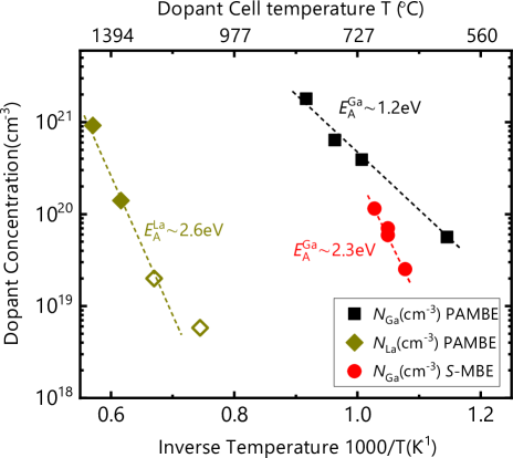
Figure 1 shows the Ga- and La-concentrations as a function of dopant cell temperature for doped samples grown using PAMBE, as well as the Ga-concentration for Ga-doped samples from S-MBE growth. An increasing cell temperature coincides with increasing dopant concentration for all dopants. These dopant concentrations follow an Arrhenius-like behavior indicating efficient incorporation of the dopants in the film. While an activation energy of eV is obtained for Ga-doped samples grown using S-MBE, i.e., without additionally supplied oxygen, the Ga activation energy obtained for samples grown using the PA-MBE method is almost two times lower. This points to a possibility that during doping with the elemental Ga source, the oxygen background during PA-MBE growth leads to the formation and subsequent evaporation of the suboxide Ga2O in the source, which has a lower activation energy in the range of 1.0-1.2 eV.25
The solubility limit of dopants in SnO was estimated from XRD. On-axis 2- scans in Figure 2 show that phase-pure, single-crystalline SnO(001) films are obtained up to the solubility limit of the various dopants. XRD data in Figure 2(a) indicate phase-pure SnO(001) samples at Ga concentrations up to cm-3. At a higher Ga content of cm-3, a weak peak due to -Ga2O3 (004) is present while the SnO related peak is absent. Similarly, in Figure 2(b), at a La concentration of cm-3, no SnO related peak is observed. Hence, in the concentration range studied, the incorporation of the extrinsic dopants was limited by the formation of secondary phases or amorphous layers. These XRD data indicate that the solubility limit of Ga and La in SnO are between cm-3 and cm-3, respectively. In Figure S1 (Supplementary material), the AFM micrographs of an nm UID layer grown at 350∘C by PA-MBE show fine and dense surface morphology films with a root-mean-square roughness of nm. Approximately 300 nm thick, PA-MBE grown, Ga-doped layers also maintained similar morphology as the UID layer, however for La doping at a similar film thickness, slightly different morphology is observed which showed an increase in roughness and less coalesced grains.
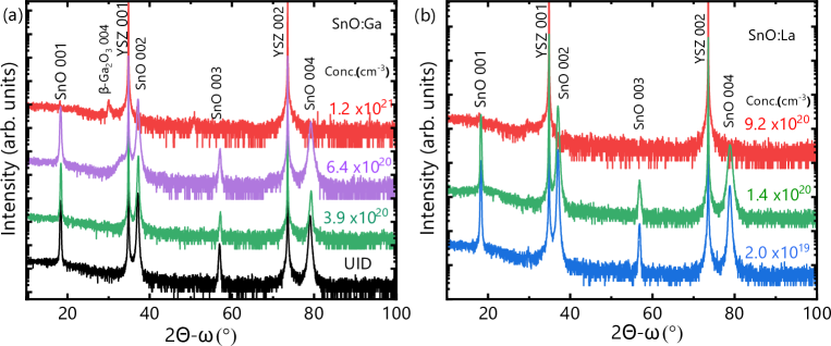
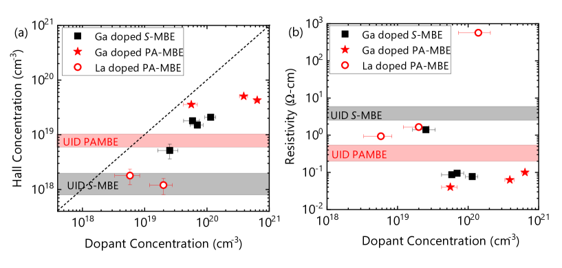
Figure 3(a) and (b) show the Hall-measured hole concentrations and resistivities, respectively, of doped SnO thin films as function of the dopant concentration. For comparison, red and black shaded areas correspond to the range of properties of UID reference samples grown for this study via PA-MBE and S-MBE, respectively. The UID -type conductivities obtained for SnO(001) layers obtained from S-MBE and PA-MBE are markedly different with higher hole concentrations for the PA-MBE grown films. This difference in transport properties for the different growth methods could be due to the enhanced formation of Sn vacancies resulting from the energetics of the different growth processes with negligible dependence on the film growth rate. For S-MBE growth, SnO molecules formed in the crucible are reaching the substrate surface, which is expected to decrease the formation of Sn vacancies and complexes compared to the PA-MBE growth, where elemental Sn and activated oxygen are supplied to the substrate. Unintentional impurities in the MBE chamber may also play a role in the UID hole concentration as these values are higher than previously reported values for MBE-grown single crystalline SnO(001).17, 26, 18
The reference UID SnO(001) layers grown for this study under different conditions by PA-MBE exhibit room temperature (RT) Hall hole concentrations () in the range of – cm-3, Hall hole mobilities () of 2.4-3.5 cm2/Vs, and bulk resistivities () of –0.2 cm. We find that increases to cm-3 and decreases to 0.063 cm for films doped with increasing amounts of Ga. SnO (001) films grown for this study by S-MBE show lower UID in the range of – cm-3,19 and –5.0 cm, increases up to cm-3 and decreases to 0.08 cm with increasing Ga doping. In contrast, thin films doped with increasing concentrations of La show a reduction in and a remarkable increase of up to 580 cm without transition to -type conductivity. Samples with higher La doping became semi-insulating and were not measurable in our Hall setup.
| Material | Grown by | UID (cm-3) | Dopant Conc. (cm-3) | Doped (cm-3) | Doped (cm ) | Ref. |
|---|---|---|---|---|---|---|
| Ga-doped SnO(poly) | sputtering | Ga | 0.27 | 27 | ||
| Na-doped SnO(poly) | sputtering | Na | 0.12 | 27 | ||
| Y-doped SnO(001) | EBE111Electron Beam Evaporation | Y | 3.8 | 17 | ||
| Sb-doped SnO(001) | EBE111Electron Beam Evaporation | Sb | 5.5 | 17 | ||
| Y-doped SnO(001) | EBE111Electron Beam Evaporation | Y | 120 | 28 | ||
| Ag-doped SnO(poly) | sputtering | Ag | 0.5 | 29 | ||
| Ga-doped SnO(001) | MBE222Molecular Beam Epitaxy | Ga = | 0.063 | This work | ||
| La-doped SnO(001) | MBE222Molecular Beam Epitaxy | La = | - | 580 | This work |
Compared to previous studies on extrinsic doping in SnO using Ga, Na, Y, Sb, and Ag and their corresponding UID films, summarized in Table I, our Ga-doped SnO shows the highest hole concentration. Closer inspection of Figure 3(a), however, suggests that dopant efficiency in SnO is limited for the range of dopants in our study. The reduction in hole concentration is weaker than the increase of La (compensating donor) concentration. Likewise, the increase of hole concentration is well below that of the Ga (acceptor) concentration, and a strong saturation of the hole density is observed with increasing Ga concentration above cm-3 in both the S-MBE and PA-MBE growths. Below a Ga concentration of cm-3, where Ga begins to form a secondary phase, transport data suggests that Ga dopants are not particularly shallow acceptors in SnO and likely not all acceptors can be ionized at RT.
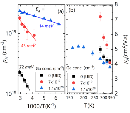
The approximate acceptor activation energies are determined from the temperature-dependent Hall measurements as shown in Figure 4 for S-MBE grown samples. The Arrhenius plot of the hole concentration for UID SnO and SnO with different Ga-doping levels indicates an apparent activation energy of 74 meV for UID SnO grown via S-MBE. The activation energy decreases from 43 meV to 14 meV with increasing Ga concentrations from cm-3 to cm-3, indicating a likely impurity band formation near the valence band with increasing acceptor doping. To estimate the UID acceptor concentration, the temperature dependent Hall data for the UID sample is extrapolated to () indicating a UID acceptor concentration of cm-3.30
The temperature dependent hole mobility in Figure 4(b) shows a strongly increasing mobility with decreasing temperature for UID SnO and Ga-doped SnO with acceptor concentrations of cm-3, indicating dominant phonon scattering. For samples with higher Ga doping of cm-3, the influence of scattering due to ionized donors, which is dominant at low temperature, led to the decrease in the mobility at low temperatures.
To explain the acceptor(donor) doping of SnO(001) with Ga(La), it is proposed that the ionic radii of the elements in different charge states promote the solubility and substitution of Ga1+ (La3+) in the Sn2+ lattice leading to the observed acceptor(donor) doping behavior31. While Ga prefers the more stable 3+ state, 1+ states have been shown to be obtainable during molecular beam epitaxy by the formation of Ga2O on the growth front or in the effusion cell.25, 32, 33 Interestingly, as shown in Table S1 (Supplementary material) the ionic radius of Ga1+ (113 pm) is close to that of Sn2+ (118 pm), while Ga3+ has a drastically different ionic radius of 62 pm. From a structural perspective, the similarity in the ionic radii of Ga1+ and Sn2+ could suggest that the substitutional incorporation of Ga1+ will be favored over Ga3+, thus promoting acceptor doping of SnO(001) with Ga. Also, La3+ with an ionic radius of 103 pm should be structurally favored over La1+ with ionic radius of 139 pm, leading to the observed compensating donor doping in SnO:La.
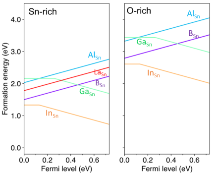
To further understand the behavior of these and other dopants, their ab-initio-calculated formation energies and charge transition levels for Sn-rich and O-rich conditions are shown in Figure 5. The results suggest that La act as a shallow donor in SnO. However experimental data indicate that semi-insulating rather than theoretically expected -type conductive films are obtained as the La concentration exceeds the UID acceptor concentration. This observation suggests that the incorporated La is being compensated by an increasing acceptor concentration relative to UID samples, such as V or related complexes. This could be a result of the Fermi level position during growth, where higher concentrations of La donors shift the Fermi level deeper into the band gap, facilitating increased incorporation of native acceptor compensators. Fig. 5 also indicates that Ga and In act most favorably as acceptors. Relative to the valence band maximum (VBM), the calculated (0/–) transition levels are 0.25 eV for Ga and 0.13 eV for In, suggesting InSn to be a more effective acceptor than Ga. While uncertainties on the order of 0.1 eV can be expected for the calculations, Ga and In acceptors are likely to exhibit incomplete ionization at room temperature. An additional (+/0) donor state exists approximately 0.02 eV below the VBM for Ga and 0.04 eV below the VBM for In, which suggests that these dopants may be effectively pinning the Fermi level in the vicinity of the VBM through self-compensation. The results are consistent with the experimental observation of a saturating hole concentration with increasing Ga doping owing to the fact that it exhibits a localized electronic character. The stabilization of 1+ oxidation states for the Ga dopant is also in contrast to the other group III dopants like Al and B, which we theoretically find to preferentially act as shallow donors. Further measurements are needed to clarify the dominant electronic contributions and ionization energies of these dopants, as well as the role of compensator species that may be simultaneously incorporated to counteract the intended doping.
In conclusion, we have shown in this study that SnO (001) can be controllably doped using La and Ga atoms. X-ray diffraction data show the solubility limits of Ga and La in SnO are between – cm-3 and – cm-3 respectively. The hole concentration increases to cm-3 and decreases to 0.063 cm for PA-MBE-grown, Ga-acceptor-doped SnO(001) films. While SnO (001) films grown via S-MBE show a lower unintentional cm-3 and, cm and increases up to cm-3 and decreases to 0.07 cm with Ga doping. In contrast, thin films doped with higher concentrations of La show a reduction in and a remarkable increase of up to 580 cm without transition to -type conductivity. Computational results identify that Ga and In preferentially act as deep acceptors with modest ionization energies in SnO, while La, Al, and B act as donors. Our results reveal that -type conductivity in SnO can be controlled by intentional Ga- and La-doping over several orders of magnitude, whereas the successful -type conduction of SnO remains challenging.
By extending the boundary of conductivity in SnO across highly conductive SnO by Ga doping and semi-insulating SnO by La doping, we demonstrated material that can be applied in a wide variety of devices: SnO-based -channel thin film transistors can thus be optimized and even tuned from normally-on (high hole concentration) to normally-off (semi-insulating SnO)34, 35. Highly conductive Ga-doped SnO can be applied in -type low resistance transparent contacts as well as promote the formation of the depletion zones inside (ultra-)wide bandgap -type oxides in heterojunction -diodes and field effect transistor devices.5 Last but not least, La-doping of SnO can lead to highly sensitive thin film conductometric gas sensors by reducing the gas-insensitive bulk conductivity of the film 36 which is electrically in parallel to the gas-sensitive, conductive surface.37
See the Supplementary material for details of the EDX measurement and AFM images of UID and doped SnO(001) thin films.
The authors thank H.-P. Schönherr and C. Hermann for MBE support, G. Hoffmann and A. Ardenghi for useful discussions and D. Dinh for critically reading the manuscript. This work was performed in the framework of GraFOx, a Leibniz-ScienceCampus partially funded by the Leibniz association. The work by J.B.V was performed under the auspices of the U.S. DOE by Lawrence Livermore National Laboratory under contract DE-AC52-07NA27344.
References
- Grundmann et al. [2016] M. Grundmann, F. Klüpfel, R. Karsthof, P. Schlupp, F.-L. Schein, D. Splith, C. Yang, S. Bitter, and H. von Wenckstern, J. Phys. D: Appl. Phys 49, 213001 (2016).
- Egbo et al. [2020] K. O. Egbo, C. E. Ekuma, C. P. Liu, and K. M. Yu, Phys. Rev. Materials 4, 104603 (2020).
- Zhang et al. [2016] K. H. L. Zhang, K. Xi, M. G. Blamire, and J. P. C. R. G. Egdell, J. Phys.: Condens. Matter 28, 383002 (2016).
- Budde et al. [2020a] M. Budde, D. Splith, P. Mazzolini, A. Tahraoui, J. Feldl, M. Ramsteiner, H. von Wenckstern, M. Grundmann, and O. Bierwagen, Appl. Phys. Lett. 117, 252106 (2020a).
- Tetzner et al. [2022] K. Tetzner, K. Egbo, M. Klupsch, R.-S. Unger, A. Popp, T.-S. Chou, S. B. Anooz, Z. Galazka, A. Trampert, O. Bierwagen, and J. W”urfl, Appl. Phys. Lett. 120, 112110 (2022).
- Parisini et al. [2022] A. Parisini, P. Mazzolini, O. Bierwagen, C. Borelli, K. Egbo, A. Sacchi, M. Bosi, L. Seravalli, A. Tahraoui, and R. Fornari, Journal of Vacuum Science & Technology A 40, 42701 (2022).
- Wang et al. [2015] Z. Wang, P. K. Nayak, A. Albar, N. Wei, U. Schwingenschlögl, and H. N. Alshareef, Advanced Materials Interfaces 2, 1500374 (2015).
- Caraveo-Frescas et al. [2013] J. A. Caraveo-Frescas, P. K. Nayak, H. A. Al-Jawhari, D. B. Granato, U. Schwingenschlögl, and A. N. . H. N. Alshareef, Acs Nano 6, 5160 (2013).
- Miller et al. [2017] S. A. Miller, P. Gorai, U. Aydemir, T. O. Mason, V. Stevanović, E. S. Toberer, and J. M. G. J. Snyder, J. Mater. Chem. C 5, 8854 (2017).
- Kim and Lee [2014] H.-J. Kim and J.-H. Lee, Sensors and Actuators B: Chemical 192, 607 (2014).
- Togo et al. [2006] A. Togo, F. Oba, I. Tanaka, and K. Tatsumi, Phys. Rev. B 74, 195128 (2006).
- Varley et al. [2013] J. B. Varley, A. Schleife, A. Janotti, and C. G. V. D. Walle, Appl. Phys. Lett. 103, 082118 (2013).
- Grauz̈inytė et al. [2018] M. Grauz̈inytė, S. Goedecker, and J. A. Flores-Livas, Phys. Rev. Materials 2, 104604 (2018).
- Granato et al. [2013] D. B. Granato, J. A. Caraveo-Frescas, H. N. Alshareef, and U. Schwingenschlögl, Appl. Phys. Lett. 102, 212105 (2013).
- Hayashi et al. [2015] H. Hayashi, S. Katayama, R. Huang, K. Kurushima, and I. Tanaka, Phys. Status Solidi RRL 9, 192 (2015).
- Hosono et al. [2011] H. Hosono, Y. Ogo, H. Yanagi, and T. Kamiya, Electrochem. Solid-State Lett. 14 (2011).
- Guo et al. [2010] W. Guo, L. Fu, Y. Zhang, K. Zhang, L. Y. Liang, Z. M. Liu, H. T. Cao, and X. Q. Pan, Appl. Phys. Lett 96, 042113 (2010).
- Budde et al. [2020b] M. Budde, P. Mazzolini, J. Feldl, C. Golz, T. Nagata, S. Ueda, G. Hoffmann, F. Hatami, W. T. Masselink, M. Ramsteiner, and O. Bierwagen, Phys. Rev. Materials 4, 124602 (2020b).
- Egbo et al. [2022] K. Egbo, E. Luna, J. Lähnemann, G. Hoffmann, A. Trampert, J. Grümbel, E. Kluth, M. Feneberg, R. Goldhahn, and O. Bierwagen, “Epitaxial synthesis of unintentionally doped -type SnO(001) via suboxide molecular beam epitaxy,” (2022).
- Hoffmann et al. [2020] G. Hoffmann, M. Budde, P. Mazzolini, and O. Bierwagen, APL Materials 8, 031110 (2020).
- Heyd et al. [2006] J. Heyd, G. E. Scuseria, and M. Ernzerhof, J. Chem. Phys 124, 219906 (2006).
- Kresse and Furthmüller [1996] G. Kresse and J. Furthmüller, Phys. Rev. B 54, 11169 (1996).
- Kresse and Joubert [1999] G. Kresse and D. Joubert, Phys. Rev. B 59, 1758 (1999).
- Blöchl [1994] P. E. Blöchl, Phys. Rev. B 50, 17953 (1994).
- Hoffmann et al. [2021] G. Hoffmann, Z. Cheng, O. Brandt, and A. M. . O. Bierwagen, APL Materials 9, 111110 (2021).
- Mei et al. [2019] A. B. Mei, L. Miao, M. J. Wahila, G. Khalsa, Z. Wang, M. Barone, N. J. Schreiber, L. E. Noskin, H. Paik, T. E. Tiwald, Q. Zheng, R. T. Haasch, D. G. Sangiovanni, L. F. J. Piper, and D. G. Schlom, Phys. Rev. Materials 3, 105202 (2019).
- Kwok et al. [2022] C. K. G. Kwok, Y. Wang, K. Egbo, and K. M. Yu, The Journal of Physical Chemistry C 126, 18963 (2022).
- Liang et al. [2012] L. Y. Liang, Z. M. Liu, H. T. Cao, W. Y. Xu, X. L. Sun, H. Luo, and K. Cang, J. Phys. D: Appl. Phys. 45, 085101 (2012).
- Pham et al. [2017] H. P. Pham, T. G. L. Thuy, Q. T. Tran, H. H. Nguyen, H. T. M. Hoa, H. T. Thu, and T. V. Cuong, Journal of Nanomaterials 2017, 1 (2017).
- White et al. [2009] M. E. White, O. Bierwagen, M. Y. Tsai, and J. S. Speck, J. Appl. Phys. 106, 93704 (2009).
- Gilardi et al. [2017] E. Gilardi, E. Fabbri, L. Bi, J. L. M. Rupp, T. Lippert, D. Pergolesi, and E. Traversa, J. Phys. Chem. C 121, 9739 (2017).
- Vogt and Bierwagen [2018] P. Vogt and O. Bierwagen, Physical Review Materials 2, 120401(R) (2018).
- Vogt et al. [2021] P. Vogt, F. V. E. Hensling, K. Azizie, C. S. Chang, D. Turner, J. Park, J. P. McCandless, H. Paik, B. J. Bocklund, G. Hoffman, O. Bierwagen, D. Jena, H. G. Xing, S. Mou, D. A. Muller, S.-L. Shang, Z.-K. Liu, and D. G. Schlom, Apl Materials 9, 031101 (2021).
- Hung et al. [2018] M. P. Hung, J. Genoe, P. Heremans, and S. Steudel, Applied Physics Letters 112, 263502 (2018).
- Zhang et al. [2022] W. Zhang, R. Hong, W. Qin, Y. Lv, J. Ma, L. Liao, K. Li, and C. Jiang, Journal of Physics: Condensed Matter 34, 404003 (2022).
- Rombach et al. [2016] J. Rombach, A. Papadogianni, M. Mischo, V. Cimalla, L. Kirste, O. Ambacher, T. Berthold, S. Krischok, M. Himmerlich, S. Selve, and O. Bierwagen, Sensors and Actuators B: Chemical 236, 909 (2016).
- Barsan et al. [2010] N. Barsan, C. Simion, T. Heine, S. Pokhrel, and U. Weimar, Journal of Electroceramics 25, 11 (2010).