Moiré pattern formation in epitaxial growth on a covalent substrate: Sb on InSb(111)A
Abstract
Structural moiré superstructures arising from two competing lattices may lead to unexpected electronic behavior, such as superconductivity or Mottness. Most investigated moiré heterostructures are based on van der Waals (vdW) materials, as strong interface interactions typically lead to the formation of strained films or regular surface reconstructions. Here we successfully synthesize ultrathin Sb films, that are predicted to show thickness-dependent topological properties, on semi-insulating InSb(111)A. Despite the covalent nature of the substrate surface, we prove by scanning transmission electron microscopy (STEM) that already the first layer of Sb atoms grows completely unstrained, while azimuthally aligned. Rather than compensating the lattice mismatch of by structural modifications, the Sb films form a pronounced moiré pattern as we evidence by scanning tunneling microscopy (STM) topography up to film thicknesses of several bilayers. Our model calculations based on density functional theory (DFT) assign the moiré pattern to a periodic surface corrugation. In agreement with DFT predictions, irrespective of the moiré modulation, the topological surface state known on thick Sb film is experimentally confirmed to persist down to low film thicknesses, and the Dirac point shifts towards lower binding energies with decreasing Sb thickness.
keywords:
moiré pattern, Sb film, InSb(111)A, topological surface state, quasi-particle interferenceThese authors contributed equally to this work \alsoaffiliationWürzburg-Dresden Cluster of Excellence ct.qmat, Universität Würzburg, D-97074 Würzburg, Germany \altaffiliationThese authors contributed equally to this work \alsoaffiliationWürzburg-Dresden Cluster of Excellence ct.qmat, Universität Würzburg, D-97074 Würzburg, Germany \altaffiliationThese authors contributed equally to this work \alsoaffiliationWürzburg-Dresden Cluster of Excellence ct.qmat, Universität Würzburg, D-97074 Würzburg, Germany \alsoaffiliationWürzburg-Dresden Cluster of Excellence ct.qmat, Universität Würzburg, D-97074 Würzburg, Germany \alsoaffiliationWürzburg-Dresden Cluster of Excellence ct.qmat, Universität Würzburg, D-97074 Würzburg, Germany \alsoaffiliationWürzburg-Dresden Cluster of Excellence ct.qmat, Universität Würzburg, D-97074 Würzburg, Germany
![[Uncaptioned image]](/html/2212.06297/assets/TOC.png)
1 Introduction
Recently the exotic properties in moiré superstructure have attracted immense research attention in the field of material physics. These can be constructed via twisting angles or lattice mismatching at the interface of layered materials.1, 2, 3 Up to now, the vast majority of studied moiré systems are based on two-dimensional (2D) materials with interlayer van der Waals (vdW) interactions,4 such as twisted bilayer graphene (TBG),5, 6 graphene/BN heterostructures,7 and transition-metal dichalcogenide (TMDC) heterostructures.8, 9, 10 Especially the band structure of TBG can be tuned by rotational twisting, inducing superconductivity or Mott insulating behavior.5, 11, 12, 13 Contrary to vdW materials, covalent materials are terminated with unsaturated dangling bonds on the surface,14 usually resulting in strong interface interaction with epitaxial films on top.15 Therefore, it is challenging to prepare moiré superstructures in a 2D film on a covalent substrate,16 however it may result in extraordinary properties, especially for a topological film.
Antimony (Sb), a material featuring strong spin-orbit coupling, has been widely investigated and proven to be a three-dimensional (3D) topological semimetal by experiment and theory.17, 18, 19 Despite coexisting with bulk carriers, its spin-polarized two-dimensional (2D) surface states are topologically protected, which has been supported by the experimental observation of high transmission rate through surface barriers such as step edges.18 Decreasing the thickness of a 3D topological insulator (TI) is known to induce a gap opening in the 2D topological surface states through the hybridization between the opposite surfaces (i.e., between surface and substrate interface) below a critical thickness.20, 21 Indeed, first principle calculations for free-standing Sb films predict a series of phase transitions upon reducing their thickness towards the few-layer regime: from the 3D topological semi-metal for bulk Sb to a 3D TI, further to a quantum spin Hall (QSH) phase, and finally to a topologically trivial semiconductor in the case of -antimonene, a single buckled honeycomb bilayer (BL) of Sb.19
The interaction with the inevitable substrate will affect the topological states of antimony films in real systems. So far, Sb films have been realized on a plethora of substrates: metal surfaces (e.g., Ag(111),22, 23, 24 Cu(111)25), 3D TIs (e.g., Bi2Se3,26, 27, 28 Bi2Te3,26, 29 Sb2Te3,26, 29 Bi2Te2Se26, 30), or semiconductor surfaces (Bi-modified Si(111),31 Ge(111)32). Most of these substrates strain the epitaxial antimony film to the corresponding substrate lattice and strongly tune its electronic properties by, e.g., interfacial charge transfer or even a topological proximity effect.30, 27 In contrast, Sb films grown on the covalent Ge(111) surface are unstrained, thereby forming an interfacial moiré pattern.32 However, the mechanism underlying this remarkable observation has not been studied in any detail so far. An additional interesting question concerns the effect of the moiré structure on the topological surface states of the Sb film.
Here, we report on the first successful preparation of Sb films on an InSb(111)A substrate by molecular beam epitaxy (MBE), with film thicknesses ranging from the few-layer limit to more than BL. Despite the covalent nature of the InSb(111) surface and very similar to the case of Ge(111), already the first Sb BL grows unstrained, i.e., does not adapt to the substrate lattice but rather assumes the lattice constant of bulk Sb, as revealed by scanning transmission electron microscopy (STEM). As seen by scanning tunneling microscopy (STM), the corresponding lattice mismatch at the interface induces a moiré pattern with an in-plane unit cell size of nm, which matches integer multiples of the lattice constants of substrate and films ( and , respectively).
In order to address the large moiré supercell with first principles calculations, we have locally approximated the stacking configuration for distinct high-symmetry sites of the supercell. In agreement with experimental evidence, these density functional theory (DFT) calculations show that the moiré pattern can be attributed to a surface corrugation of the Sb films which is observable even for film thicknesses of several BLs. The calculations demonstrate that the unstrained configuration is energetically more stable than a model in which the Sb film is strained to the InSb(111) substrate. Additionally, DFT reveals that a topological surface state, which has been proven on bulk Sb,17, 18 is preserved above a critical thickness. This is experimentally confirmed by the observation of quasi-particle interference probed by scanning tunneling spectroscopy (STS). Experiment and theory also agree on a shift of the surface state’s Dirac point towards lower binding energies with decreasing film thickness.
2 Results and discussion
For the epitaxial growth of our Sb films we start from a clean InSb(111)A (i.e., indium-terminated) substrate surface of reconstruction (see Figure S1), obtained by cycles of Ar+ sputtering and a subsequent anneal to C. After Sb deposition, islands with thicknesses ranging from BL to BL, dependent on the duration of evaporation, form on the InSb(111)A surface (Figure S2). While the outline of the first Sb BL is mostly arbitrary, all further layers crystallize in a pyramid-like triangular shape. Around the Sb islands, a Sb wetting layer forms which can be removed without affecting the Sb islands by post-annealing to C (Figure 1a). The anneal exposes the clean InSb(111)A substrate surface in a Sb-rich surface reconstruction of periodicity.33 The line profile across several steps of the Sb layers in Figure 1b allows to determine the step height between two Sb terraces to nm, in good agreement to the single atomic step height of bulk Sb in the [111] orientation 34. The step height of the first Sb layer to the substrate is nm. This difference could be attributed to either a different bond length between substrate and Sb layers compared to the bond length between Sb layers or to the fact that STM does not show the actual topography of the surface but rather a mixture of topography and the local density of states (LDOS). The right most step with height of 0.38 nm comes from the substrate, which can be identified from the obvious reconstruction on top and also corresponds well to the known single-step height height of InSb(111).35 Figure 1c shows the close-up image of a BL terrace with atomic resolution of the Sb lattice and an additional superimposed intensity modulation that can be attributed to the moiré pattern. The symmetry and lattice constant of the surface unit cell of nm (Figure 1d) is identical to that of the (111) surface of a pristine Sb crystal.34 Therefore, the Sb films are determined to be composed of vertically stacked -antimonene layers (called antimonene in the remainder of this paper), in which the Sb atoms form a buckled honeycomb lattice as depicted in Figure 1e.
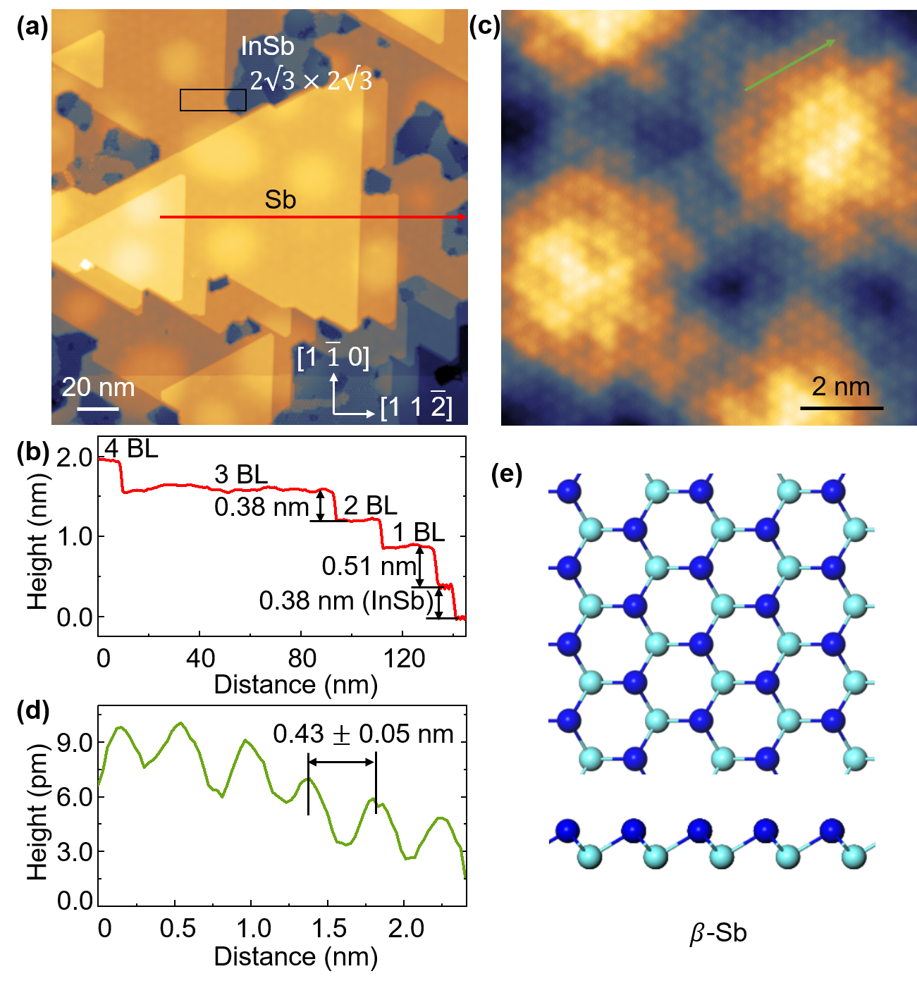
For further insight into the origin of the moiré superstructure, Figure 2a shows an STM image of the hexagonal moiré lattice, which is acquired on a BL Sb island. Each moiré unit cell (green rhombus) shows one section of maximal intensity and two sections with local intensity minima, similar to the moiré superstructures in TBG and TMDC systems.36, 37, 8 Cross-sectional STEM is used to obtain the side view of the interface, shown in Figure 2b. It is apparent that the Sb film does not adapt to the periodicity of the substrate but rather assumes the lattice constant of its bulk structure. This finding is rather unusual for a covalent substrate, like InSb(111)A, which possesses energetically unfavorable unsaturated dangling bond states at its In-terminated surface that are prone to form covalent bonds. The strong tendency of Sb to bond with itself rather than with a covalent substrate has already been reported for Sb films on Ge(111) which also show a lattice mismatch induced moiré pattern.32 Such behaviour can be understood by considering the energy required to strain free-standing Sb layers to the larger (smaller) lattice constant of the InSb(111) (Ge(111)) substrates. Our 1x1 calculations indicate that adopting to the InSb(111) lattice constant with the ideal stacking position is energetically less favorable for the Sb films than retaining the free-standing lattice constant (see section III in Supporting Information). Interestingly, bismuth (Bi), another group V element, was also recently reported to grow on InSb(111) without adapting to the substrates lattice.38 However, rather than forming a moiré structure as in the case of Sb, the ultra thin Bi films were found to relieve their lattice mismatch-induced strain by forming a Sierpiński structure. These two different ways of strain relief suggest that compared to Bi, Sb forms stronger intra-layer bonds, which keep the bulk structure of Sb fully intact already from the first bilayer.
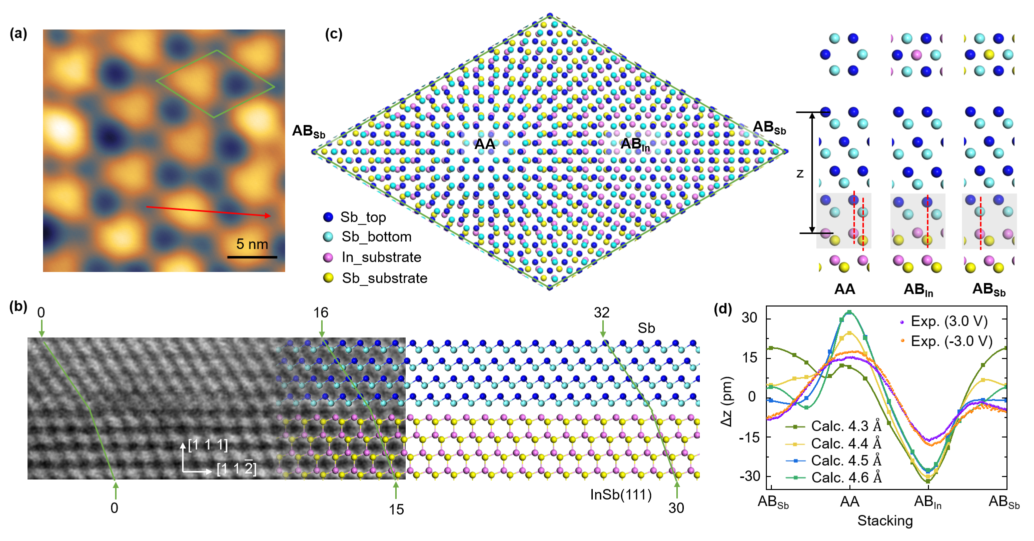
It is noteworthy, that after Sb deposition the substrate shows a bulk lattice configuration at the interface, as seen by STEM, which indicates that the Sb growth suppresses the surface reconstruction of the clean substrate and stabilizes the atomic configuration of its bulk. Therefore, even though there is no adaptation of the lattice structures, an interaction of both materials at the interface takes place. STEM unambiguously shows that the lattice mismatch-induced moiré pattern forms immediately at the film-substrate interface, i.e., already at the first Sb bilayer, rather than between two adjacent Sb layers within the film. Additionally, the lattices of the substrate and Sb films are azimuthally aligned to each other, i.e., the moiré pattern is not generated by a rotational misalignment of substrate and Sb films. In total, Sb lattice constants (nm) cover lattice constants of InSb(111)A (nm), forming the moiré superlattice of nm seen in STM. Further confirmation for the rotational alignment of the lattices is provided by the STM topographies which simultaneously show the atomic lattices of the Sb films and of the substrate (Figure 1a and Figure S4).
Figure 2c shows the atomic representation of the moiré situation at the interface in top view which is limited, for the sake of clarity, to a single layer of antimonene on top of the InSb(111)A surface layer. In this moiré supercell, three local atomic geometries of distinct symmetries can be identified, labeled here as AA, AB and AB. The notation is adapted from that used for bilayer graphene and TMDCs 8, 39 and denotes by the index which atom species of the lower lattice remains uncovered by the upper lattice in top view. For AA, the atomic positions of both lattices match while for AB (AB), the In (Sb) substrate atoms are (in top view) centered in the honeycombs of the first antimonene bilayer of the film (see schematic atomic structure in Figure 2c).
For a better understanding of the interfacial bonding situation and the mechanism underlying the moiré pattern formation we now turn to a theoretical analysis. We will start by looking at the different local bonding situations, i.e., by performing DFT calculations for simple lattices whose unit cell represents the various interface alignments. This approach explicitly excludes interactions between the different stacking configurations in the full moiré lattice. The analysis of the latter would require the simulation of the full Sb on InSb moiré unit cell, for which a brute-force systematic ab-initio simulation is computationally out of reach. Despite the local approximation, these calculations allow for a surprisingly accurate inspection of the stacking-dependent electronic and structural properties, as we demonstrate in the following.
By comparison of the relaxed atomic structures of different sites inside the moiré unit cell, it becomes evident that the height of the Sb adatoms above the substrate (visualized in Figure 2d) varies for different stacking configurations. In our primitive cell calculations, substrate and film possess the same in-plane lattice parameter for which we assumed various values between those of bulk InSb(111) (Å) and bulk Sb (Å). In Figure 2d we show the resulting theoretical height profiles for a BL Sb film in comparison to their experimental counterparts. These profiles are taken along the horizontal diagonal of a moiré unit cell (cf. Figure 2c), covering all high-symmetry sites (i.e., from AB on the left corner via AA and AB to the next AB on the right corner). Both experiment and theory find a maximal (minimal) corrugation at the AA (AB) stacking. The height for the AB alignment is instead sensitively affected by the lattice constant, which is plausible as this is the portion of the unit cell experiencing the strongest interface interaction (more detail further below). In contrast to the experimental moiré structure, the bonding described by this simplified approach strongly depends on the film’s and substrate’s local strain. Notwithstanding this limitation, it is able to satisfactorily describe the overall trend in the observed structural pattern.
In this context we wish to point out that the STM data is robust against a variation of the tunneling voltage (purple and orange curves in Figure 2d are acquired at V and V, respectively), demonstrating that the measured line profile is dominated by the surface topography and not by variations in the local density of states. A similar height trend of the calculated interface Sb layer, i.e., the first BL Sb film, is shown in Figure S5. These results show that the moiré pattern manifests itself as an atomic height modulation between interface and first Sb layer, which translates to surface corrugations even for several bilayers, similar to the Sb/Ge(111) case.32 As expected, the corrugation of the moiré pattern decreases with increasing layer thickness (see Figures S2, S8, and S9). The overall good agreement between theory and experiment suggests that the moiré surface corrugation is mostly driven by the local stacking energies, with long-range interactions being of only minor importance.
| bond length [nm] | AA | AB | AB |
|---|---|---|---|
| SbIn | |||
| SbSb | |||
| SbIn | |||
| SbSb | |||
| SbSb |

The local atomic models for the BL Sb films on InSb(111) additionally allow us to take a closer look at the bond length between the substrate and the Sb films at the high-symmetry sites (Table 1). For AA and AB, the shortest bond between substrate and Sb film is found to be nm (Sb atom of substrate to the bottom Sb atom of Sb layer) and nm (In atom of substrate to the bottom Sb atom of Sb layer), respectively. Both are much larger than the intra-bilayer Sb-Sb bonds (nm), indicating a weak interaction at the interface. In contrast, the AB geometry corresponds to a regular continuation of InSb(111) with the bottom Sb atom on top of the In atom at the interface, resulting in the shortest interfacial bond length (nm) within the moiré supercell. For stackings close to AB, the dominating interface bond is close to the Sb intra-bilayer distances of 0.29 nm, hereby indicating a much stronger interaction with the substrate.
Having established the local substrate-Sb bonding conditions, the influence on the electronic properties will be investigated in the following with the focus on the Sb-surfaces. The surface states of Sb thick films connect conduction and valence states. With decreasing thickness, the surface and interface film layers interact more strongly, resulting in a hybridization gap and Rashba-type surface states (see Figures S6 and S7). This transition occurs below thicknesses of 4 and 5 BL depending on the high-symmetry position, determined by the interplay of substrate/interface-Sb interaction and Sb surface/interface interaction (see Figures S6 and S7).
As shown in the band structure of Figure 3 for AB, the top Sb surface state (indicated in yellow) moves down w.r.t. to the Fermi level with increasing film thickness. The same height-dependent trend is also found for most of the sites inside the moiré supercell including the high-symmetry AA layering (Figures S6 and S7). For stackings close to AB the opposite trend is observed, where the Sb surface state shifts up in energy with increasing thickness (see Figures S6 and S7). In contrast, the energy positions of the interface states colored with red in Figures 3, S6 and S7 are determined by the stacking configuration and are barely influenced by the film thickness.
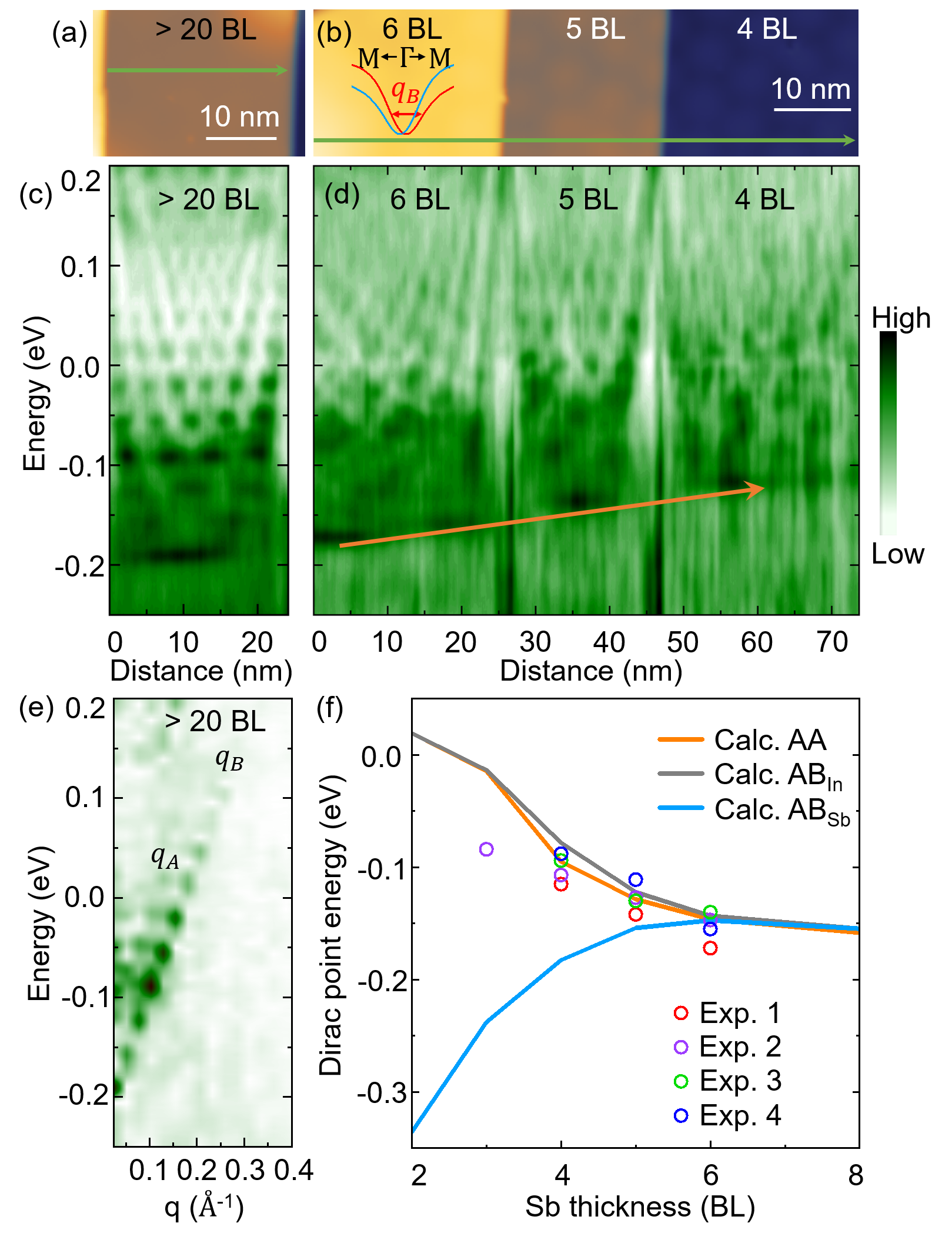
In order to study the thickness-dependent evolution of the electronic structure of Sb films experimentally, we performed scanning tunneling spectroscopy (STS) measurements. Spectra are acquired on Sb terraces of varying thickness ( BL, BL) along lines perpendicular to Sb step edges, as depicted by green arrows in Figures 4a and b. The corresponding spatially resolved variation of the local density of state (LDOS) is shown in Figures 4c and d, respectively. The spectra taken on a thick Sb film ( BL) show a standing wave pattern similar to that observed on the (111) surface of a single crystal of Sb by Seo et al.18 For bulk Sb, this quasiparticle interference (QPI) pattern is generated by the scattering of the two-dimensional topological surface state from adjacent parallel step edges. The dominant scattering vector q is shown in the inset in Figure 4b (red arrow) and connects surface states with the same spin (see the detailed scattering geometry in Ref. 18). A fast Fourier transform (FFT) (Figure 4e) of the spectra in Figures 4c confirms that the scattering features coincide with that observed for the topological surface state on bulk Sb. For lower film thickness, the interference pattern is still visible but become blurrier and the background intensity stronger (Figure 4d). We attribute this trend to the increasing surface corrugation of the moiré pattern towards lower thickness, which may induce additional scattering centers for the surface state. The fact that the QPI is still visible for few-layer Sb films indicates that a surface state, similar to that of bulk Sb, is preserved despite the presence of a substrate.
Finally, the QPI pattern also allows to extract the position of the surface state’s Dirac point. For the thick Sb film ( BL), the Dirac point is located at meV, slightly higher than that of bulk Sb meV, which may be attributed to the influence of the substrate. For BL, BL, and BL Sb, we find the Dirac point at mV, mV, and mV, respectively, indicating a shift towards lower binding energies with decreasing thickness (see Figure 4f for the experimental data measured in various sample areas). This thickness-dependent trend of the Dirac point is also predicted by our DFT calculations for most local stacking configurations with topological nontrivial surface states, i.e., AA, AB, and other non-high-symmetry stackings, while calculations close to AB stackings show the opposite trend. However, as stated before, AB is a unique local area that shows rather strong substrate-Sb interaction and particular electronic properties inside the moiré unit cell. According to the experimentally observed trend of the Dirac point and the calculation results, we can assume, that the Sb films of BL on InSb(111)A preserve the general topological properties theoretically predicted for most sites of the film, typified by AA and AB sites.
Unfortunately, due to the rather 3D growth which prevents thickness-dependent angle-resolved photoelectron spectroscopy (ARPES) studies and the influence of the moiré pattern on Sb films of low thickness, our experimental data can not provide information about a thickness-dependent topological phase transition as predicted by DFT calculations. On the other hand, moiré superstructures are recently extensively studied in twisted bilayer graphene or TMDCs due to their rich physics, such as flat bands and quantum-confined electronic states40, 41, 39, 42, 43. A moiré pattern on a covalent surface could therefore evoke interesting properties which deserve further studies with more elaborated theoretical models.
3 Conclusion
In summary, we successfully synthesized high-quality Sb films on a covalent InSb(111)A substrate with thicknesses down to the few-layer limit. The Sb layers do not adapt their lattice to the covalent substrate, but keep their bulk Sb lattice structure already from the first deposited bilayer, thereby generating a lattice-mismatch induced moiré pattern with a supercell lattice constant of nm. Our DFT calculations for specific local stacking geometries occurring throughout the supercell provide support for an energetic stabilization of the moiré pattern compared to the case of strained Sb film. These calculations also show that the Rashba-type surface states of the few BL films transform above a critical film thickness into the 2D topological surface states known from bulk Sb. The existence and thickness evolution of these surface states, i.e., shifting towards lower binding energy as decreasing Sb thickness, are experimentally confirmed by the detection of corresponding QPI patterns using STS. Our work not only introduces a new substrate for the epitaxy of ultrathin Sb films, but also provides first insights into the mechanism underlying the surprising occurrence of a lattice mismatch-induced moiré structure on a covalent substrate.
4 Methods
Sb with high purity (99.9999 ) was evaporated from a Knudsen cell with the substrate held at C. All STM data was acquired with a commercial Omicron LT-STM at K. Cross-sectional lamellae for STEM investigations were prepared on a Dual-Beam System (FEI Helios Nanolab) equipped with an Omniprobe micromanipulator. Scanning transmission electron microscopy was performed using an uncorrected FEI Titan 80-300 operating at kV, pA beam current and a convergence semi-angle of mrad. The images were recorded using a high-angle annular dark-field electron detector.
The theoretical studies of local structures with different stackings and numbers of Sb layers were carried out with first-principle density functional calculations as implemented in the Vienna ab initio simulation package (VASP) 44, within the projector augmented-plane-wave (PAW) method 45, 46. For the exchange-correlation potential the PBE-GGA functional 47 was used, by expanding the Kohn-Sham wave functions into plane waves up to an energy cutoff of eV. We sample the Brillouin zone on a Monkhorst-Pack mesh and employ spin-orbit coupling self-consistently 48.
We consider two-dimensional systems of 6 InSb BL with hydrogen-passivated Sb-termination (B face) and BL to BL of Sb on the In-terminated (A face) surface with different in-plane alignments. To disentangle the electronic states of both surfaces, a vacuum distance of at least Å between periodic replicas in z-direction is applied. The structures are relaxed vertically to the surface until forces converged below eV/Å. The height of the InSb bilayers are strained to Å to exhibit a band gap similar to calculations of the bulk substrate with hybrid functionals as HSE06.49 The relative alignment between film and substrate bands might be influenced by this approach, however the effect of the substrate on the general trends and behaviour of the surface state should be negligible.
This work has been funded by the Deutsche Forschungsgemeinschaft (DFG, German Research Foundation) through the Würzburg-Dresden Cluster of Excellence EXC2147 on Complexity and Topology in Quantum Matter ct.qmat (Project ID 390858490) as well as through the Collaborative Research Center SFB 1170 ToCoTronics (Project ID 258499086). B.L. gratefully acknowledges support by the Alexander von Humboldt Foundation, Bonn, Germany. G.S. and S.E. acknowledge the support from the Deutsche Forschungsgemeinschaft (DFG, German Science Foundation) through FOR 5249-449872909 (Project P5). S. E., P. E. and G.S. thank Domenico Di Sante for useful discussions.
The following files are available free of charge.
-
•
InSb(111)A surface, as-grown Sb islands, energetic analysis of Sb films on InSb(111)A substrate, orientation of moiré pattern, calculated bond length, height and band structures of Sb films, moiré intensity and fast Fourier transform (FFT) results
References
- Cao et al. 2020 Cao, Y.; Rodan-Legrain, D.; Rubies-Bigorda, O.; Park, J. M.; Watanabe, K.; Taniguchi, T.; Jarillo-Herrero, P. Tunable correlated states and spin-polarized phases in twisted bilayer–bilayer graphene. Nature 2020, 583, 215–220
- Pierce et al. 2021 Pierce, A. T.; Xie, Y.; Park, J. M.; Khalaf, E.; Lee, S. H.; Cao, Y.; Parker, D. E.; Forrester, P. R.; Chen, S.; Watanabe, K., et al. Unconventional sequence of correlated Chern insulators in magic-angle twisted bilayer graphene. Nat. Phys. 2021, 17, 1210–1215
- Liu et al. 2021 Liu, Y.; Zeng, C.; Yu, J.; Zhong, J.; Li, B.; Zhang, Z.; Liu, Z.; Wang, Z. M.; Pan, A.; Duan, X. Moiré superlattices and related moiré excitons in twisted van der Waals heterostructures. Chem. Soc. Rev. 2021, 50, 6401–6422
- Geim and Grigorieva 2013 Geim, A. K.; Grigorieva, I. V. van der Waals heterostructures. Nature 2013, 499, 419–425
- Cao et al. 2018 Cao, Y.; Fatemi, V.; Fang, S.; Watanabe, K.; Taniguchi, T.; Kaxiras, E.; Jarillo-Herrero, P. Unconventional superconductivity in magic-angle graphene superlattices. Nature 2018, 556, 43–50
- Nimbalkar and Kim 2020 Nimbalkar, A.; Kim, H. Opportunities and challenges in twisted bilayer graphene: a review. Nano-Micro Lett. 2020, 12, 1–20
- Dean et al. 2013 Dean, C. R.; Wang, L.; Maher, P.; Forsythe, C.; Ghahari, F.; Gao, Y.; Katoch, J.; Ishigami, M.; Moon, P.; Koshino, M., et al. Hofstadter’s butterfly and the fractal quantum Hall effect in moiré superlattices. Nature 2013, 497, 598–602
- Zhang et al. 2017 Zhang, C.; Chuu, C.-P.; Ren, X.; Li, M.-Y.; Li, L.-J.; Jin, C.; Chou, M.-Y.; Shih, C.-K. Interlayer couplings, moiré patterns, and 2D electronic superlattices in MoS2/WSe2 hetero-bilayers. Sci. Adv. 2017, 3, e1601459
- Tang et al. 2020 Tang, Y.; Li, L.; Li, T.; Xu, Y.; Liu, S.; Barmak, K.; Watanabe, K.; Taniguchi, T.; MacDonald, A. H.; Shan, J., et al. Simulation of Hubbard model physics in WSe2/WS2 moiré superlattices. Nature 2020, 579, 353–358
- Seyler et al. 2019 Seyler, K. L.; Rivera, P.; Yu, H.; Wilson, N. P.; Ray, E. L.; Mandrus, D. G.; Yan, J.; Yao, W.; Xu, X. Signatures of moiré-trapped valley excitons in MoSe2/WSe2 heterobilayers. Nature 2019, 567, 66–70
- Yankowitz et al. 2019 Yankowitz, M.; Chen, S.; Polshyn, H.; Zhang, Y.; Watanabe, K.; Taniguchi, T.; Graf, D.; Young, A. F.; Dean, C. R. Tuning superconductivity in twisted bilayer graphene. Science 2019, 363, 1059–1064
- Po et al. 2018 Po, H. C.; Zou, L.; Vishwanath, A.; Senthil, T. Origin of Mott insulating behavior and superconductivity in twisted bilayer graphene. Phys. Rev. X 2018, 8, 031089
- Chen et al. 2021 Chen, B.-B.; Liao, Y. D.; Chen, Z.; Vafek, O.; Kang, J.; Li, W.; Meng, Z. Y. Realization of topological Mott insulator in a twisted bilayer graphene lattice model. Nat. Commun. 2021, 12, 1–7
- Gatos 1961 Gatos, H. C. Dangling bonds in III–V compounds. J. Appl. Phys. 1961, 32, 1232–1234
- Xu et al. 2018 Xu, C.-Z.; Chan, Y.-H.; Chen, P.; Wang, X.; Flötotto, D.; Hlevyack, J. A.; Bian, G.; Mo, S.-K.; Chou, M.-Y.; Chiang, T.-C. Gapped electronic structure of epitaxial stanene on InSb(111). Phys. Rev. B 2018, 97, 035122
- Bian et al. 2022 Bian, M.; Zhu, L.; Wang, X.; Choi, J.; Chopdekar, R. V.; Wei, S.; Wu, L.; Huai, C.; Marga, A.; Yang, Q., et al. Dative epitaxy of commensurate monocrystalline covalent van der Waals moiré supercrystal. Adv. Mater. 2022, 34, 2200117
- Hsieh et al. 2009 Hsieh, D.; Xia, Y.; Wray, L.; Qian, D.; Pal, A.; Dil, J. H.; Osterwalder, J.; Meier, F.; Bihlmayer, G.; Kane, C. L.; Hor, Y. S.; Cava, R. J.; Hasan, M. Z. Observation of unconventional quantum spin textures in topological insulators. Science 2009, 323, 919
- Seo et al. 2010 Seo, J.; Roushan, P.; Beidenkopf, H.; Hor, Y. S.; Cava, R. J.; Yazdani, A. Transmission of topological surface states through surface barriers. Nature 2010, 466, 343–346
- Zhang et al. 2012 Zhang, P.; Liu, Z.; Duan, W.; Liu, F.; Wu, J. Topological and electronic transitions in a Sb(111) nanofilm: The interplay between quantum confinement and surface effect. Phys. Rev. B 2012, 85, 201410
- Li et al. 2010 Li, Y.-Y.; Wang, G.; Zhu, X.-G.; Liu, M.-H.; Ye, C.; Chen, X.; Wang, Y.-Y.; He, K.; Wang, L.-L.; Ma, X.-C., et al. Intrinsic topological insulator Bi2Te3 thin films on Si and their thickness limit. Adv. Mater. 2010, 22, 4002–4007
- Zhang et al. 2010 Zhang, Y.; He, K.; Chang, C.-Z.; Song, C.-L.; Wang, L.-L.; Chen, X.; Jia, J.-F.; Fang, Z.; Dai, X.; Shan, W.-Y.; Shen, S.-Q.; Niu, Q.; Qi, X.-L.; Zhang, S.-C.; Ma, X.-C.; Xue, Q.-K. Crossover of the three-dimensional topological insulator Bi2Se3 to the two-dimensional limit. Nat. Phys. 2010, 6, 584–588
- Mao et al. 2018 Mao, Y.-H.; Zhang, L.-F.; Wang, H.-L.; Shan, H.; Zhai, X.-F.; Hu, Z.-P.; Zhao, A.-D.; Wang, B. Epitaxial growth of highly strained antimonene on Ag(111). Front. Phys. 2018, 13, 138106
- Shao et al. 2018 Shao, Y.; Liu, Z.-L.; Cheng, C.; Wu, X.; Liu, H.; Liu, C.; Wang, J.-O.; Zhu, S.-Y.; Wang, Y.-Q.; Shi, D.-X.; Ibrahim, K.; Sun, J.-T.; Wang, Y.-L.; Gao, H.-J. Epitaxial growth of flat antimonene monolayer: A new honeycomb analogue of graphene. Nano Lett. 2018, 18, 2133–2139
- Sun et al. 2020 Sun, S.; Yang, T.; Luo, Y. Z.; Gou, J.; Huang, Y.; Gu, C.; Ma, Z.; Lian, X.; Duan, S.; Wee, A. T. S.; Lai, M.; Zhang, J. L.; Feng, Y. P.; Chen, W. Realization of a buckled antimonene monolayer on Ag(111) via surface engineering. J. Phys. Chem. Lett. 2020, 11, 8976–8982
- Zhu et al. 2019 Zhu, S.-Y.; Shao, Y.; Wang, E.; Cao, L.; Li, X.-Y.; Liu, Z.-L.; Liu, C.; Liu, L.-W.; Wang, J.-O.; Ibrahim, K.; Sun, J.-T.; Wang, Y.-L.; Du, S.; Gao, H.-J. Evidence of topological edge states in buckled antimonene monolayers. Nano Lett. 2019, 19, 6323–6329
- Jin et al. 2016 Jin, K.-H.; Yeom, H. W.; Jhi, S.-H. Band structure engineering of topological insulator heterojunctions. Phys. Rev. B 2016, 93, 075308
- Holtgrewe et al. 2020 Holtgrewe, K.; Mahatha, S.; Sheverdyaeva, P.; Moras, P.; Flammini, R.; Colonna, S.; Ronci, F.; Papagno, M.; Barla, A.; Petaccia, L., et al. Topologization of -antimonene on Bi2Se3 via proximity effects. Sci. Rep. 2020, 10, 1–12
- Hogan et al. 2019 Hogan, C.; Holtgrewe, K.; Ronci, F.; Colonna, S.; Sanna, S.; Moras, P.; Sheverdyaeva, P. M.; Mahatha, S.; Papagno, M.; Aliev, Z. S.; Babanly, M.; Chulkov, E. V.; Carbone, C.; Flammini, R. Temperature driven phase transition at the antimonene/Bi2Se3 van der Waals heterostructure. ACS Nano 2019, 13, 10481–10489
- Lei et al. 2016 Lei, T.; Liu, C.; Zhao, J.-L.; Li, J.-M.; Li, Y.-P.; Wang, J.-O.; Wu, R.; Qian, H.-J.; Wang, H.-Q.; Ibrahim, K. Electronic structure of antimonene grown on Sb2Te3 (111) and Bi2Te3 substrates. J. Appl. Phys. 2016, 119, 015302
- Kim et al. 2016 Kim, S. H.; Jin, K.-H.; Park, J.; Kim, J. S.; Jhi, S.-H.; Yeom, H. W. Topological phase transition and quantum spin Hall edge states of antimony few layers. Sci. Rep. 2016, 6, 33193
- Yao et al. 2013 Yao, G.; Luo, Z.; Pan, F.; Xu, W.; Feng, Y. P.; Wang, X.-s. Evolution of topological surface states in antimony ultra-thin films. Sci. Rep. 2013, 3, 2010
- Fortin-Deschênes et al. 2017 Fortin-Deschênes, M.; Waller, O.; Mentes, T.; Locatelli, A.; Mukherjee, S.; Genuzio, F.; Levesque, P.; Hébert, A.; Martel, R.; Moutanabbir, O. Synthesis of antimonene on germanium. Nano Lett. 2017, 17, 4970–4975
- Nishizawa et al. 1998 Nishizawa, M.; Eguchi, T.; Misima, T.; Nakamura, J.; Osaka, T. Structure of the surface and its dynamical formation processes. Phys. Rev. B 1998, 57, 6317–6320
- Chekmazov et al. 2015 Chekmazov, S. V.; Bozhko, S. I.; Smirnov, A. A.; Ionov, A. M.; Kapustin, A. A. STM/STS study of the Sb(111) surface. Phys. Procedia 2015, 71, 323–326
- Li et al. 2020 Li, J.; Tang, C.; Du, P.; Jiang, Y.; Zhang, Y.; Zhao, X.; Gong, Q.; Kou, X. Epitaxial growth of lattice-matched InSb/CdTe heterostructures on the GaAs(111) substrate by molecular beam epitaxy. Appl. Phys. Lett. 2020, 116, 122102
- Xie et al. 2019 Xie, Y.; Lian, B.; Jäck, B.; Liu, X.; Chiu, C.-L.; Watanabe, K.; Taniguchi, T.; Bernevig, B. A.; Yazdani, A. Spectroscopic signatures of many-body correlations in magic-angle twisted bilayer graphene. Nature 2019, 572, 101–105
- Bistritzer and MacDonald 2011 Bistritzer, R.; MacDonald, A. H. Moiré bands in twisted double-layer graphene. Proc. Natl. Acad. Sci. 2011, 108, 12233–12237
- Liu et al. 2021 Liu, C.; Zhou, Y.; Wang, G.; Yin, Y.; Li, C.; Huang, H.; Guan, D.; Li, Y.; Wang, S.; Zheng, H.; Liu, C.; Han, Y.; Evans, J. W.; Liu, F.; Jia, J. Sierpiński structure and electronic topology in Bi thin films on InSb(111)B surfaces. Phys. Rev. Lett. 2021, 126, 176102
- Kim et al. 2017 Kim, K.; DaSilva, A.; Huang, S.; Fallahazad, B.; Larentis, S.; Taniguchi, T.; Watanabe, K.; LeRoy, B. J.; MacDonald, A. H.; Tutuc, E. Tunable moiré bands and strong correlations in small-twist-angle bilayer graphene. Proc. Natl. Acad. Sci. 2017, 114, 3364–3369
- Cao et al. 2018 Cao, Y.; Fatemi, V.; Demir, A.; Fang, S.; Tomarken, S. L.; Luo, J. Y.; Sanchez-Yamagishi, J. D.; Watanabe, K.; Taniguchi, T.; Kaxiras, E.; Ashoori, R. C.; Jarillo-Herrero, P. Correlated insulator behaviour at half-filling in magic-angle graphene superlattices. Nature 2018, 556, 80–84
- Cao et al. 2018 Cao, Y.; Fatemi, V.; Fang, S.; Watanabe, K.; Taniguchi, T.; Kaxiras, E.; Jarillo-Herrero, P. Unconventional superconductivity in magic-angle graphene superlattices. Nature 2018, 556, 43–50
- Li et al. 2021 Li, H.; Li, S.; Naik, M. H.; Xie, J.; Li, X.; Regan, E.; Wang, D.; Zhao, W.; Yumigeta, K.; Blei, M., et al. Imaging local discharge cascades for correlated electrons in WS2/WSe2 moiré superlattices. Nat. Phys. 2021, 17, 1114–1119
- Pan et al. 2018 Pan, Y.; Fölsch, S.; Nie, Y.; Waters, D.; Lin, Y.-C.; Jariwala, B.; Zhang, K.; Cho, K.; Robinson, J. A.; Feenstra, R. M. Quantum-confined electronic states arising from the moiré pattern of MoS2–WSe2 heterobilayers. Nano Lett. 2018, 18, 1849–1855
- Kresse and Furthmüller 1996 Kresse, G.; Furthmüller, J. Efficient iterative schemes for ab initio total-energy calculations using a plane-wave basis set. Phys. Rev. B 1996, 54, 11169–11186
- Kresse and Joubert 1999 Kresse, G.; Joubert, D. From ultrasoft pseudopotentials to the projector augmented-wave method. Phys. Rev. B 1999, 59, 1758–1775
- Blöchl 1994 Blöchl, P. E. Projector augmented-wave method. Phys. Rev. B 1994, 50, 17953–17979
- Perdew et al. 1996 Perdew, J. P.; Burke, K.; Ernzerhof, M. Generalized gradient approximation made simple. Phys. Rev. Lett. 1996, 77, 3865–3868
- Steiner et al. 2016 Steiner, S.; Khmelevskyi, S.; Marsmann, M.; Kresse, G. Calculation of the magnetic anisotropy with projected-augmented-wave methodology and the case study of disordered alloys. Phys. Rev. B 2016, 93, 224425
- Hilal et al. 2016 Hilal, M.; Rashid, B.; Khan, S. H.; Khan, A. Investigation of electro-optical properties of InSb under the influence of spin-orbit interaction at room temperature. Mater. Chem. Phys. 2016, 184, 41–48