\alsoaffiliation

Programmable Functional Materials Lab, Brain and Consciousness Research Center, Moscow, 121205, Russia \alsoaffiliationProgrammable Functional Materials Lab, Brain and Consciousness Research Center, Moscow, 121205, Russia \alsoaffiliationProgrammable Functional Materials Lab, Brain and Consciousness Research Center, Moscow, 121205, Russia

Supplementary Materials for ”Ultralow-noise terahertz detection by p-n junctions in gapped bilayer graphene”

Elena Titova Center for Photonics and 2D Materials, Moscow Institute of Physics and Technology, Dolgoprudny, 141700, Russian Federation titova.elenet@gmail.com    Dmitry Mylnikov Center for Photonics and 2D Materials, Moscow Institute of Physics and Technology, Dolgoprudny, 141700, Russian Federation    Mikhail Kashchenko Center for Photonics and 2D Materials, Moscow Institute of Physics and Technology, Dolgoprudny, 141700, Russian Federation    Sergey Zhukov Center for Photonics and 2D Materials, Moscow Institute of Physics and Technology, Dolgoprudny, 141700, Russian Federation    Kirill Dzhikirba Institute of Solid State Physics, RAS, Chernogolovka 142432, Russian Federation    Kostya Novoselov Institute for Functional Intelligent Materials, National University of Singapore, Singapore, 117575, Singapore    Denis Bandurin Department of Materials Science and Engineering, National University of Singapore, 117575 Singapore    Georgy Alymov Center for Photonics and 2D Materials, Moscow Institute of Physics and Technology, Dolgoprudny, 141700, Russian Federation    Dmitry Svintsov Center for Photonics and 2D Materials, Moscow Institute of Physics and Technology, Dolgoprudny, 141700, Russian Federation

SI I. Device fabrication

Refer to caption
Figure S1: hBN-BLG-hBN stack and lithography-defined contacts of the sample A
Refer to caption
Figure S2: hBN-BLG-hBN stack, metal contacts and final view of the sample B (we measured the right-placed device)

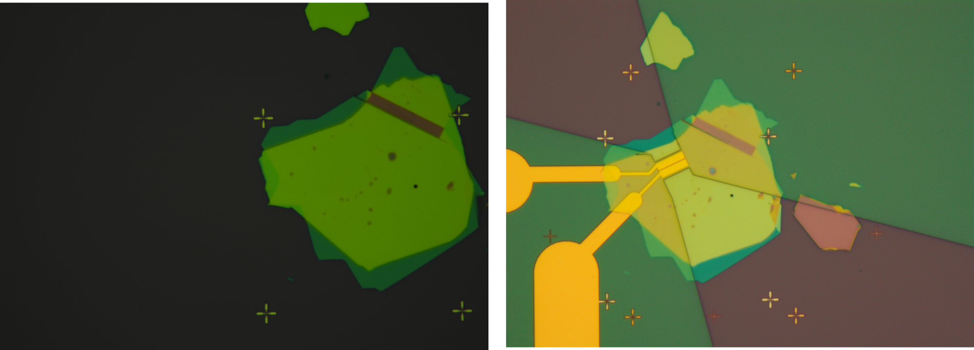
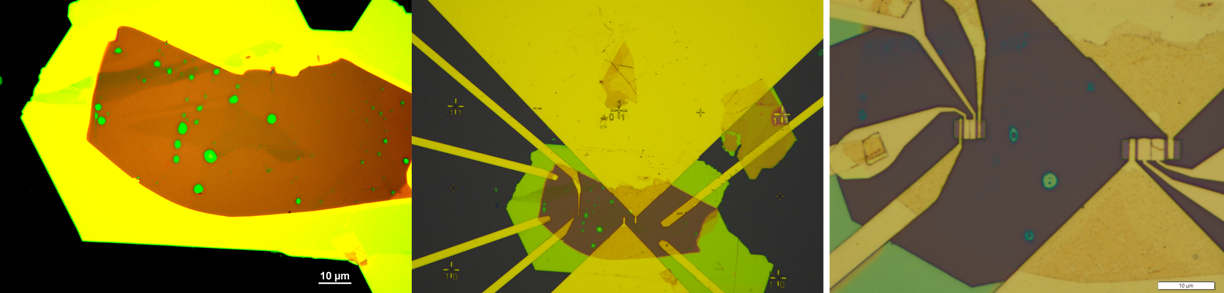
BLG flakes were identified after exfoliation by optical contrast using an optical microscope. Hexagonal boron nitride (hBN) flakes about 50nm thick were exfoliated from hBN bulk crystals and found in the same way as graphene flakes. We used e-beam lithography with PMMA A4, developing in cold IPA:DI water 3:1 and DI water as a stopper. After developing we etched the sample in oxygen plasma of 150W for 2-3s to remove residual resist in developed windows. To define the channel shapes we etched hBN-graphene outside of the future transistor channel in SF6 plasma. Ti/Au metal contacts was deposited by electron beam sputtering followed by a lift-off process in acetone. We did three rounds of electron lithography to fabricate the device - the first to make the top gates, the second to sputter the drain-source contacts, and the third to etch the excess hBN and graphene from the sample.

SII II. THz source calibration

Refer to caption
Figure S3: Integrated power of our 130 GHz source and 140 GHz reference source at a modulation frequency of 23 Hz, scanned by a #1 pyroelectric detector mounted on a motorized x-y stage.
Refer to caption
Figure S4: Measured THz source beam angle distribution in vertical and horizontal planes along with a Gaussian fit with σ=10o𝜎superscript10𝑜\sigma=10^{o}.

SIII III. Measurements

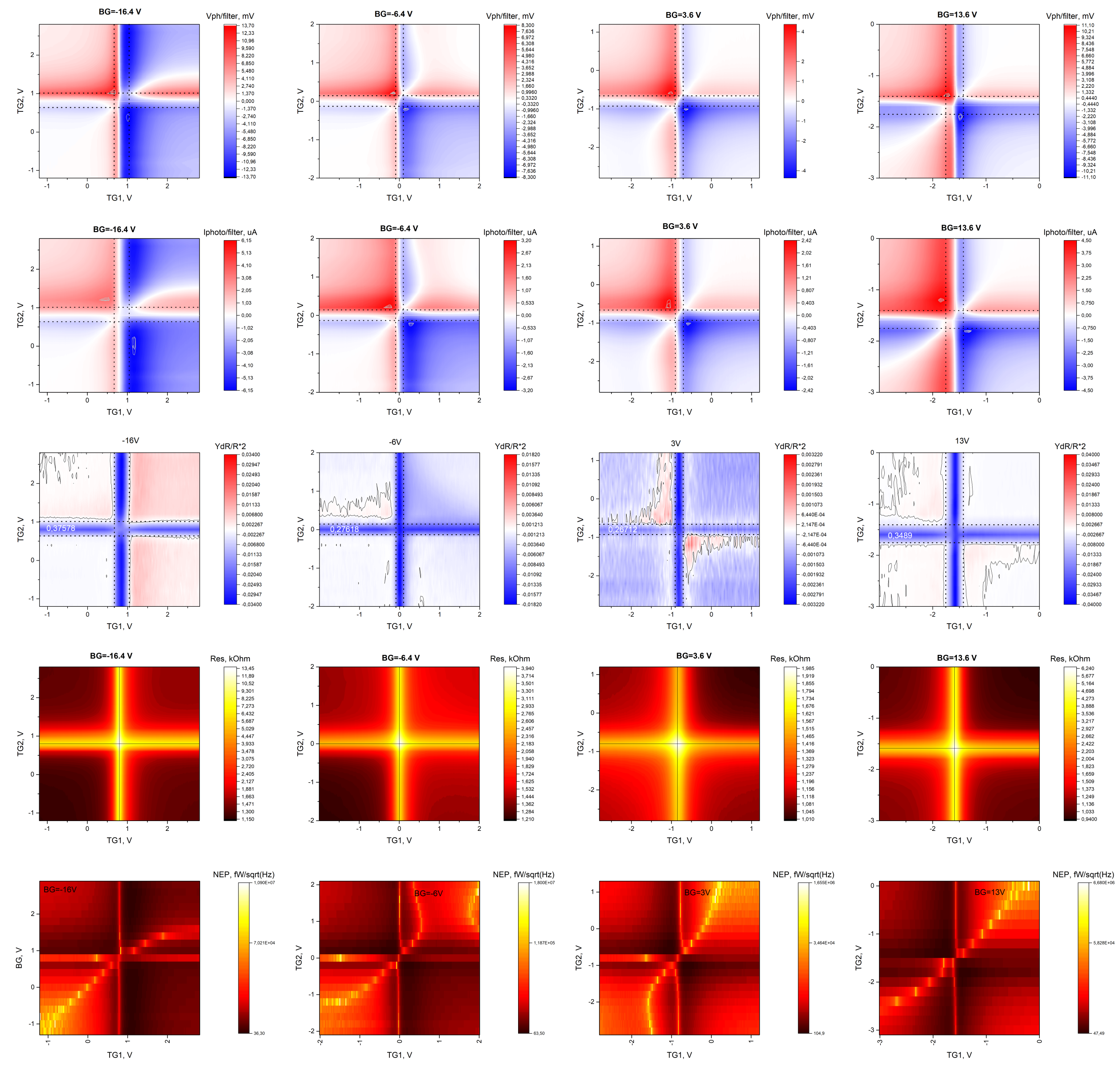
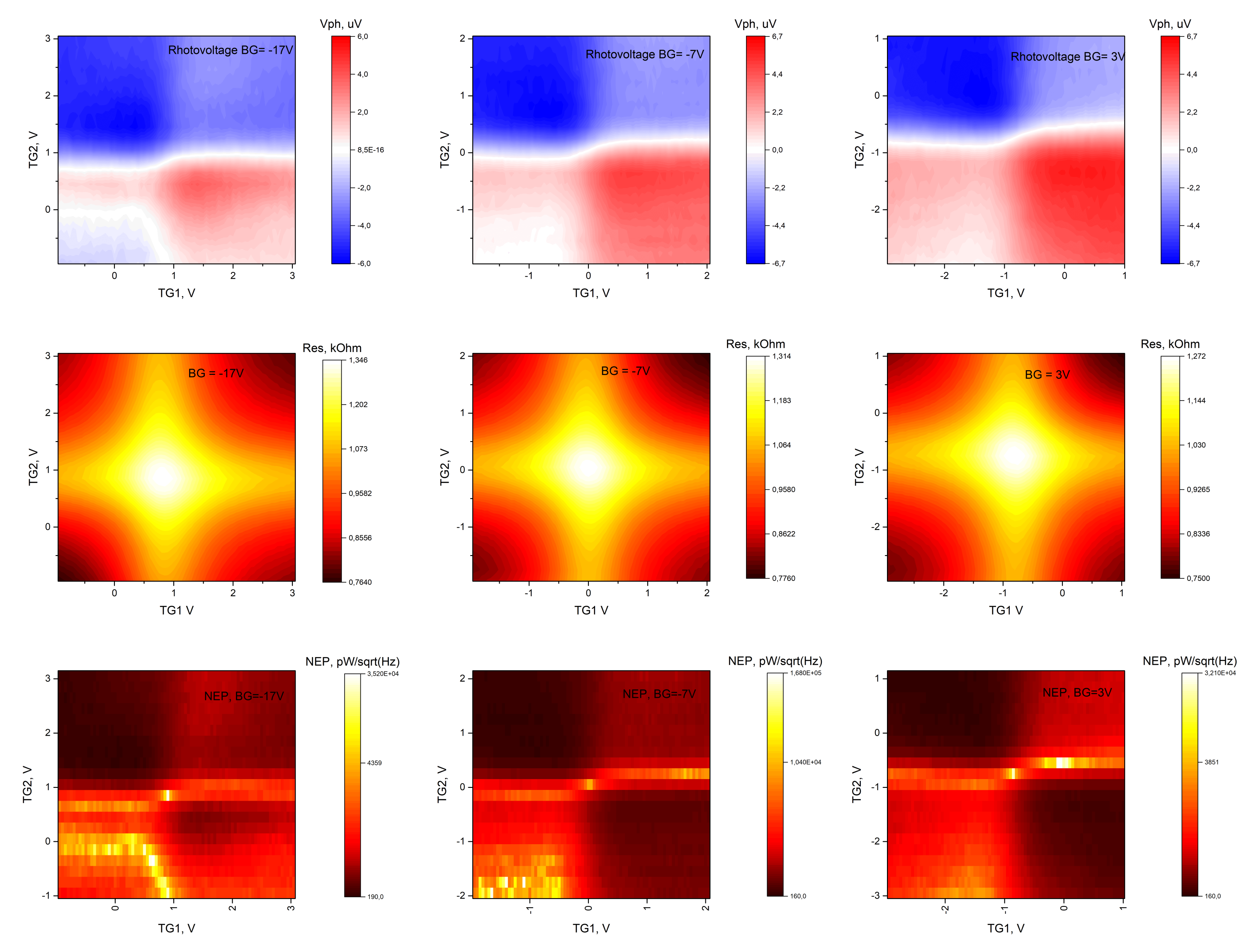
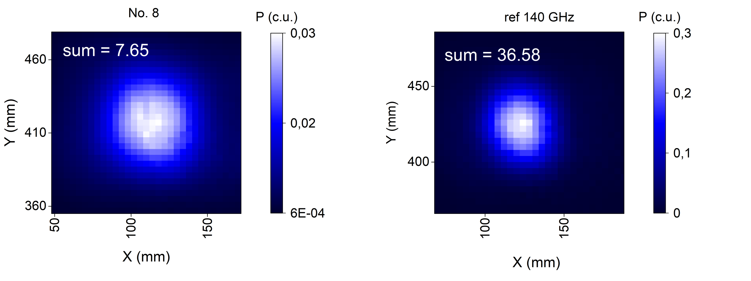
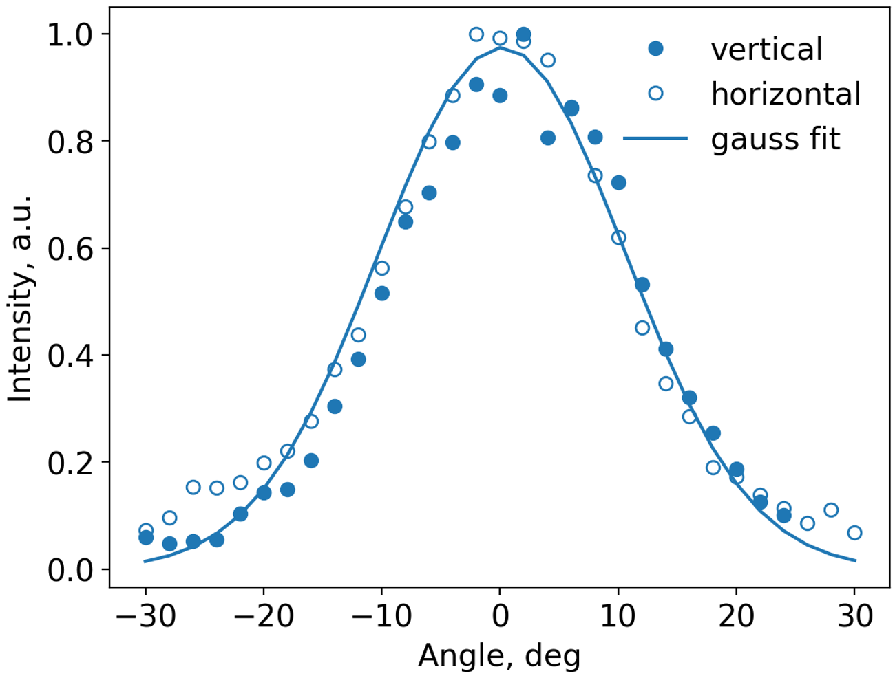
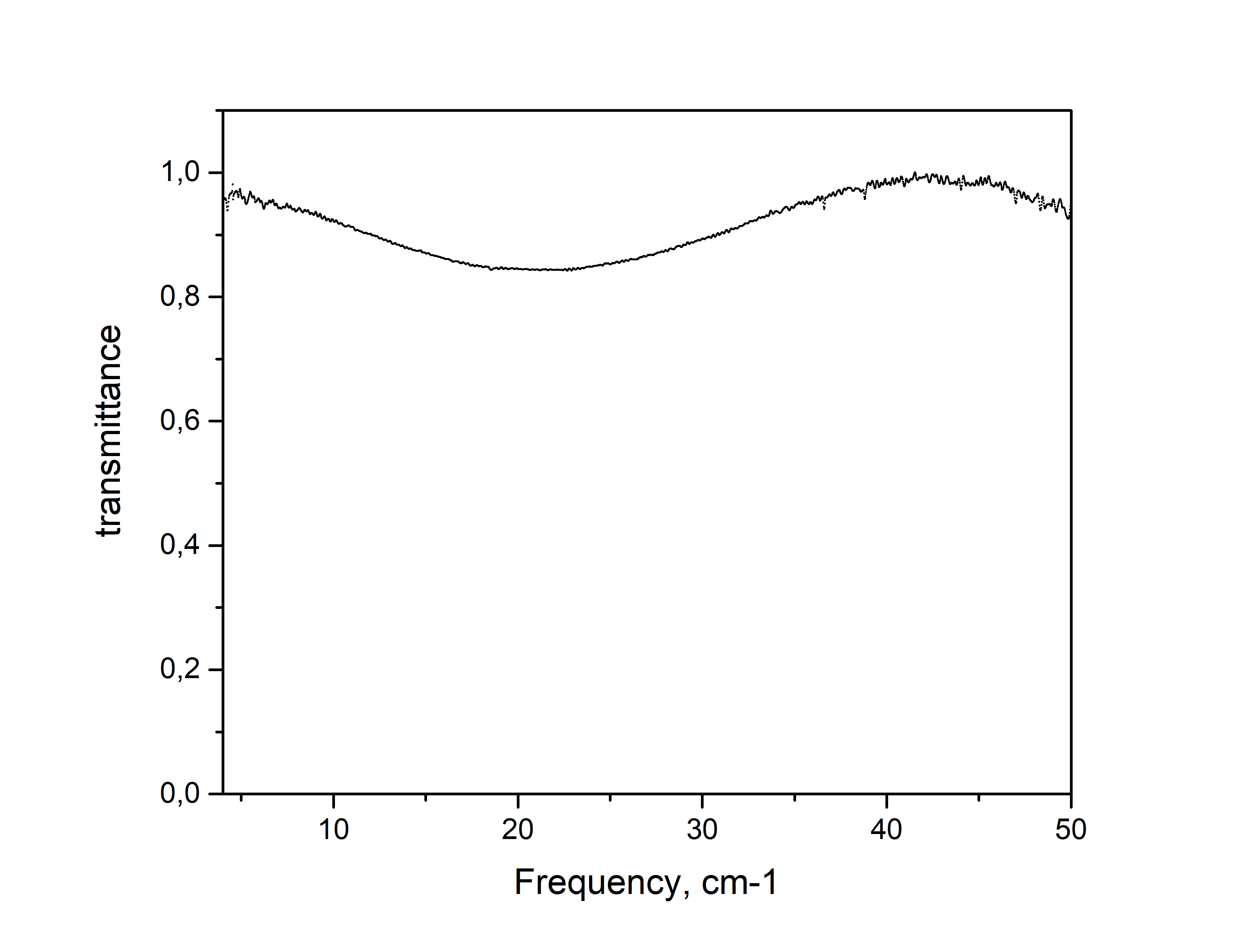
The pressure inside the cryostat was maintained no more than 1e-5hPa. We used 0.13 THz IMPATT-diode source with horn antenna output. We characterized sample A in a completely symmetrical configuration, applying Isd/2subscript𝐼𝑠𝑑2-I_{sd}/2 and +Isd/2subscript𝐼𝑠𝑑2+I_{sd}/2 to the source and drain, respectively, and measured all parameters (Rsd,Vphsubscript𝑅sdsubscript𝑉phR_{\rm s-d},V_{\rm ph} and δR𝛿𝑅\delta R) simultaneously as differential signals VdVssubscript𝑉𝑑subscript𝑉𝑠V_{d}-V_{s}. Sample B was characterized with grounded source, and we measured in series the resistance and then the photovoltage from this sample. Sample A was measured without Si lens at a distance of about 19 cm from the THz source, using filter with transmittance 0.03, and polarizer at 45osuperscript45𝑜45^{o} having the transmittance 0.5. We considered the sample absorption cross section to be equal to the maximum possible, resting on the fundamental limit 111Mylnikov, D.; Svintsov, D. Physical Review Applied 2022, 17, 064055. 3/2λ2/4π0.6mm232superscript𝜆24𝜋0.6𝑚superscript𝑚23/2\cdot\lambda^{2}/4\pi\approx 0.6mm^{2}, so we present here the values of photoresponsivity and equivalent noise power estimated from below. Sample B was measured with Si lens 12mm in diameter, and the sample was located at a distance of 17.5 cm from the THz source, filter 0.003, and the same polarizer angle, set parallel to the antenna. Assuming the lens focuses all radiation into a spot smaller than antenna (1mm21𝑚superscript𝑚21mm^{2}), we also considered the reflectance of external radiation from the lens surface (26%). The total power reached the sample B is P0=340nWsubscript𝑃0340𝑛𝑊P_{\rm 0}=340nW

Refer to caption
Figure S5: Transmittance of window material for cryostat - mylar film. It has an almost constant transmittance, about 100%.

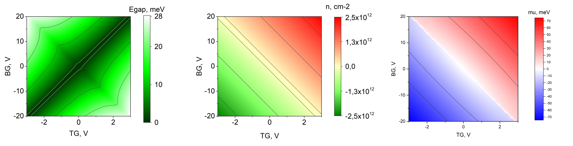
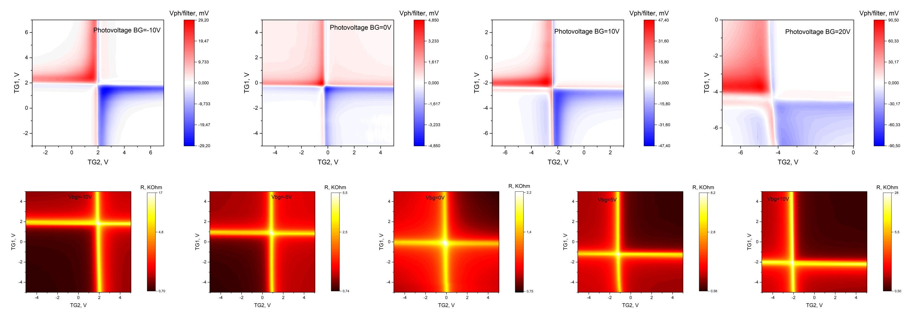
SIV IV.Additional results

Refer to caption
Figure S6: Photovoltage, photocurrent, photoresistance, source-to-drain resistance and NEP for the sample A at different fixed back gate voltages at 25K.
Refer to caption
Figure S7: Photovoltage, source-to-drain resistance and NEP for the sample A at different fixed back gate voltages at 300K.
Refer to caption
Figure S8: Calculated values of band gap, concentration and chemical potential as a function of top and back gate voltages
Refer to caption
Figure S9: Photovoltage and source-to-drain resistance for the sample B at different fixed back gate voltages at 25K.