Evaluation of HPK - planar pixel sensors for the CMS Phase-2 upgrade
Abstract
To cope with the challenging environment of the planned high luminosity upgrade of the Large Hadron Collider (HL-LHC), scheduled to start operation in 2029, CMS will replace its entire tracking system. The requirements for the tracker are largely determined by the long operation time of 10 years with an instantaneous peak luminosity of up to in the ultimate performance scenario. Depending on the radial distance from the interaction point, the silicon sensors will receive a particle fluence corresponding to a non-ionizing energy loss of up to . This paper focuses on planar pixel sensor design and qualification up to a fluence of .
For the development of appropriate planar pixel sensors an R&D program was initiated, which includes - sensors on (6”) wafers with an active thickness of with pixel sizes of and manufactured by Hamamatsu. Single chip modules with ROC4Sens and RD53A readout chips were made. Irradiation with protons and neutrons, as well was an extensive test beam campaign at DESY were carried out. This paper presents the investigation of various assemblies mainly with ROC4Sens readout chips. It demonstrates that multiple designs fulfill the requirements in terms of breakdown voltage, leakage current and efficiency. The single point resolution for pixels is measured as for non-irradiated samples, and after irradiation to .
keywords:
Pixel , Silicon , Sensors , CMS , HL-LHC , Radiation hardness.1 Introduction
To increase the potential for discoveries at the Large Hadron Collider (LHC) after Run 3, a significant luminosity increase of the accelerator is targeted [1]. CERN therefore plans to upgrade the machine to the high-luminosity configuration (HL-LHC) during the Long Shutdown 3 (LS3), scheduled for the years 2026-28, with the goal of achieving a peak luminosity of nominal, or even in the ultimate performance scenario assumed in the following. The machine is expected to run at a center-of-mass energy of with a bunch-crossing separation of and a maximum average of 200 collisions (pileup) per bunch crossing. For an expected 10 year operation of the HL-LHC, the CMS experiment aims to collect an integrated luminosity of . To maintain or even improve the performance of CMS in this harsh environment, the detector will undergo several upgrades during the next years. In particular, the entire Inner Tracker (IT), which is based on silicon pixel modules, will be replaced [2].
The IT will consist of four barrel layers (TBPX) and twelve forward disks (TFPX and TEPX), which themselves consist of up to 5 rings, at each end of the barrel to extend tracking to a pseudorapidity || = 4. The innermost barrel layer has a radius of , while for the other layers the radii are . The layers and disks are composed of modular detector units, consisting of silicon pixel sensors bump bonded to readout chips. In order to simplify detector construction and integration and to minimize the number of required spares, only two types of detector modules are foreseen, namely modules with and modules with readout chips.
In the innermost pixel layer, a fluence of particles corresponding to a non-ionising energy loss (NIEL) of a neutron equivalent fluence of and a total ionizing dose (TID) of will be reached after ten years of operation. To cope with these radiation levels, a readout chip using the TSMC 65 nm CMOS technology [3] is under development within the RD53 Collaboration [4]. The chip will have a non-staggered bump bond pattern with pitch, which allows a reduction of the pixel area by a factor of six compared to the current detector, thus improving the spatial resolution and reducing the cluster merging, e.g. in boosted jets or due to pileup events. For the studies presented in this paper, an R&D readout chip is used, the ROC4Sens [5], which is introduced in Sec. 2.2.1.
Radiation induced bulk damage leads to an increase of leakage current, changes of the electric field and a signal reduction due to charge carrier trapping [6, 7]. Planar silicon pixel sensors are the baseline choice for the entire pixel detector except for the innermost barrel layer, where 3D sensors are chosen due to their higher radiation tolerance and lower power dissipation. The maximum fluence for planar sensors will be reached in ring 1 of TFPX. For the full lifetime of the IT, with delivered, the fluence in this ring is expected to reach , while in ring 2 of TFPX and barrel layer 2 fluences of and are expected, respectively. The IT is constructed such that ring 1 in TFPX could be exchanged after half of the lifetime, which would result in a maximum fluence of about . At the time of writing it has not yet been decided whether TFPX ring 1 will be exchanged. It should also be noted that the fluence in the endcaps depends strongly on the radial distance from the beam line. The above quoted numbers refer to the maximum fluence, received at the inner module edge, while the mean fluence over the module is much lower, about over the full detector lifetime. The CMS readout chip has been tested up to a total ionizing dose of 10 MGy. Tests at the dose level of 15 MGy, expected for the detector region equipped with planar sensors for the full detector lifetime, are planned for 2023. This paper focuses on the characterization of planar silicon pixel sensors for fluences up to the maximum expected in a scenario with exchange of TFPX ring 1, namely . For this, pixel sensors with an active thickness of are required to achieve a hit efficiency of at least 99%, with a signal to threshold ratio of 3 or more.
The best spatial resolution is achieved when the projected charge is distributed over two pixels. The CMS Inner Tracker operates in a magnetic field of , which results in a strong Lorentz deflection in the direction orthogonal to the magnetic field and the electrical field , distributing the signal over two or more pixels in the barrel layers. For example, for a sensor thickness of and a Lorentz angle of this deflection amounts to . This means that for pixels with a pitch of the Lorentz angle has to be reduced by decreasing the mobility, which in turn requires a higher electrical field. For the configuration of thickness and pitch mentioned above, a straightforward estimate using the relationship between field-dependent mobility and Lorentz drift yields a bias voltage of about in the case of - sensors.
Overall, the sensor concept must allow for: a) operation at high bias voltage without electrical breakdown before irradiation, b) operation at up to 800 V to achieve the required hit efficiency after irradation, and c) operation without sparking between chip and sensor.
This paper presents the R&D program for planar silicon pixel sensors produced by Hamamatsu Photonics K.K. (HPK) [8] with the aim of obtaining sensors that meet the criteria for the CMS Inner Tracker as given in Table 1.
| Parameter | Value | Measured at |
|---|---|---|
| Polarity | - | |
| Active thickness | ||
| Breakdown voltage | 300 V | non-irradiated |
| Breakdown voltage | 800 V | > |
| Leakage current | ||
| at + 50 V | ||
| Leakage current | ||
| at 600 V | > | |
| Hit , before irradiation | 99% | + 50 V |
| Hit | 99% | , |
| Hit | 98% | , |
The paper is structured as follows. In Section 2 a detailed description of the pixel sensor layout is given. The sample preparation including irradiations is described in Section 3. The beam test setup and data analysis are presented in Sections 4 and 5. Finally, the results and conclusions are reported in Sections 6 and 7.
2 Sensor description
A brief and preliminary outline of the first sensor production of planar pixel sensors by HPK for this project can be found in Ref. [10]. In the following, a more comprehensive overview is given.
2.1 Technological choices
The goal of this production was mainly to evaluate different silicon substrates and to optimise the pixel layout. For this purpose, different types of - sensors were produced on a total of 35 high-resistivity (6”) -type float zone wafers with crystal orientation <100>. The decision for - sensors instead of - used in the current CMS pixel detector is not based on higher radiation hardness (after type-inversion the performance of both types is similar), but on the fact that - sensor production requires only a single-sided lithography and therefore is potentially cheaper and offered by more vendors. An inherent disadvantage of this approach is the risk for sparks to form between the sensor edges and the readout chip at high voltages (Section 3.2). To solve this issue, additional processing steps during bump bonding or module production are needed, which partially reduces the advantages of the - approach.
The active thickness of the wafers is chosen to be . For sensors with this thickness, a minimum ionising particle creates about electron-hole pairs (most probable value) [11]. A reduction by 60% is expected after the fluence collected in 10 years of operation, leading to an expected charge of 4400 electrons. As the final chip is designed to work with an in-time threshold of around electrons and with built-in data sparsification, the module would still have a signal/threshold ratio of about 3 for barrel layers 2-4 and for the disks at the end of operation.
To fabricate the pixel sensors three substrate options have been investigated:
-
1.
float zone thinned (FTH150),
-
2.
float zone Si-Si direct bonded (FDB150),
-
3.
and float zone deep diffused (FDD150).
The production of the FTH150 material starts with the same material and thickness as HPK’s standard thick sensors, which is a thick float zone with an approximately thick backside implant. After most of the frontside processing, the backside is mechanically thinned down to the final thickness. Since the frontside has already been processed, there is a limitation on the temperature and annealing time for the backside implant to avoid deformation of the front junction, so that the backside implant is much shallower compared to HPK’s standard sensors. As a result, the backside of these sensors has a higher sensitivity to scratches, which can lead to a high leakage current in case the depletion region touches the backside. The effect of such high leakage currents on the module production of large sensors must be evaluated.
The FDB150 material is obtained by bonding together two wafers: a high resistivity float zone wafer and a low resistivity handle wafer, which is usually manufactured with the Czochralski method. The float zone wafer is thinned down to an active thickness of . After processing the handle wafer is thinned down to , resulting in a total thickness of . Compared to the FTH150 wafers, the FDB150 wafers are more expensive to produce but less sensitive to scratches and handling, which should lead to a higher module yield.
The processing of the FDD150 material is similar to the processing of standard float zone material, but with a much deeper backside implant. Due to this deeper implant, a more gradual transition from the low-resistivity to the high-resistivity bulk is achieved compared to the direct-bonded or thinned material [12]. The diffusion parameters are chosen such that an active layer of is reached and then the wafer is thinned down to . It is known that deep diffusion can introduce material defects [13] and possibly dislocations during processing, which can lead to radial as well as axial non-uniform doping distributions.
On the -side of the sensor, which is the structured electrode side, an inter-pixel isolation is required to isolate neighbouring pixels. For this production, both -stop and -spray isolation were considered as options. For the -spray isolation, a maskless process was chosen, which, in contrast to the moderated -spray technique used for the current CMS barrel pixel sensors [14], does not require an additional mask. Since HPK prefers the -stop technique for reasons of production reliability, only a few wafers were produced with the -spray option.
The bulk resistivity was specified to be 3-5 kcm. All wafers were processed with a metal grid on the backside to allow light injection. A summary of the wafer specifications is given in Table 2.
| Parameter | Value |
|---|---|
| Silicon wafer diameter | (6”) |
| Wafer type | -type, float zone (FZ) |
| Crystal orientation | <100> |
| Active thickness | |
| Total thickness | (FDB/FDD), (FTH) |
| Resistivity | 3 – 5 kcm |
| Oxygen concentration | – |
| Number of FTH wafers | 10 (-stop) |
| Number of FDB wafers | 10 (-stop) + 10 (-spray) |
| Number of FDD wafers | 5 (-stop) |
2.2 Mask layouts
Two different mask sets were produced, one for the wafers with -stop isolation and one for the wafers with -spray isolation. Each mask set contains designs of pixel sensors compatible with different readout chips (bond patterns) and a variety of test structures, such as diodes of different sizes and shapes, MOS-capacitors, MOSFETs and gate-controlled diodes. A picture of a fully processed -stop wafer is shown in Fig. 1.
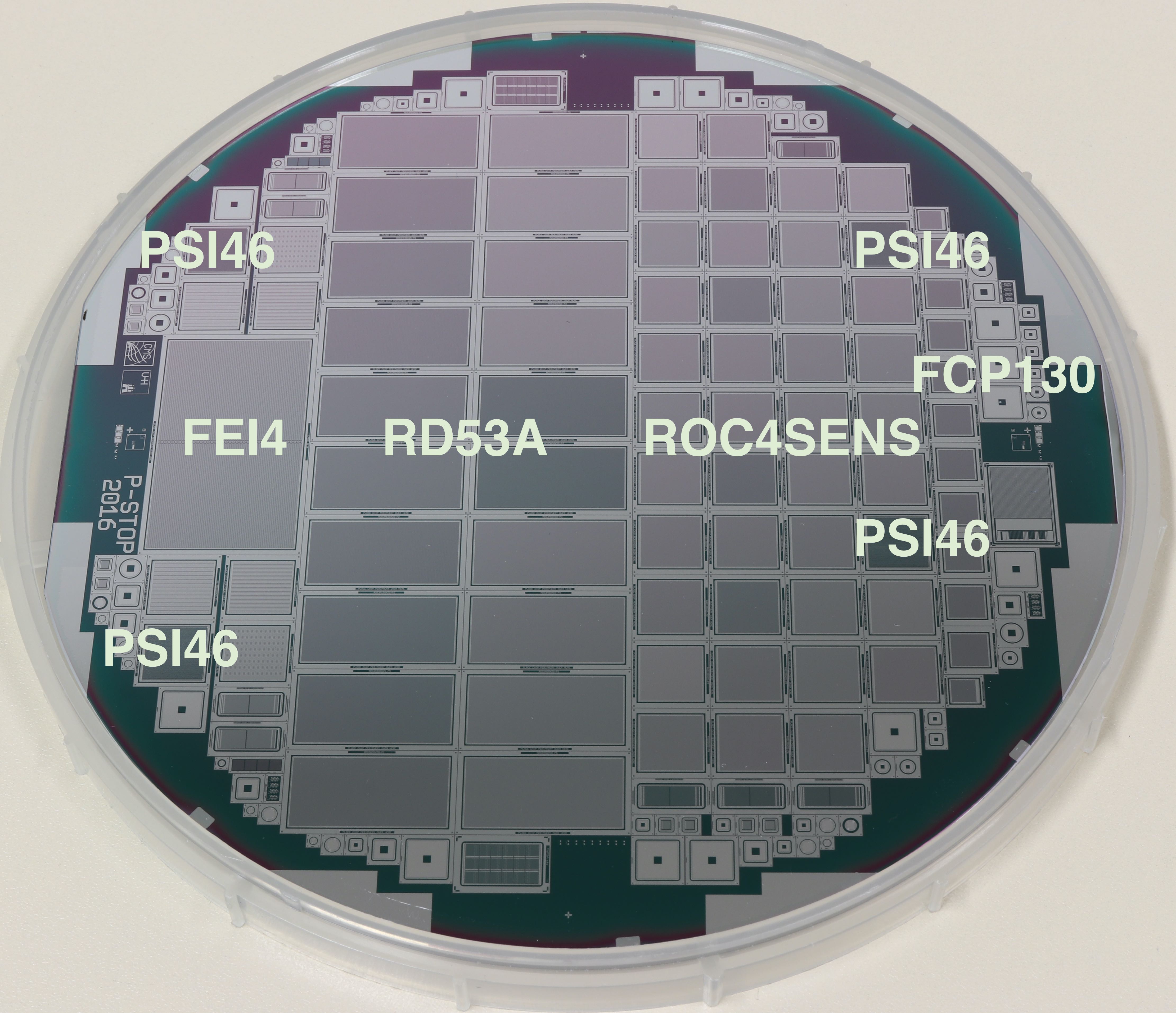
As neither the ROC4Sens nor the RD53A chip, both with pitch (see below), were available at the time of wafer design, sensors compatible with the PSI46 chip [15], which has a bump bond pattern of , and sensors compatible with the FE-I4 chip [16], whose bump bond pattern is , were processed as fallback options. The sensors designed for the FE-I4 chip were implemented as one double sensor (compatible with two chips) in the -stop mask, and as two single sensors in the -spray mask. Sensors compatible with the PSI46 chip were designed with the default readout pattern of , but also with a metal routing structure which allows reading out and subcells. Since these structures were not bump bonded to readout chips, these designs will not be discussed further in the following.
To achieve a high yield during module production, only sensors that fulfil (before irradiation) the specifications given in Table 1 should be used. In order to obtain meaningful results from a current-voltage (–) measurement of a pixelated sensor on the wafer before bump bonding, a bias structure is required to keep all pixel cells on the same potential. After testing, the bias structure is in general not needed anymore and one aim of this production is to find a bias structure that has a minimal impact on the charge collection and is compatible with high voltage operation after irradiation. For this purpose, sensors with common punch-through (PT) structures, polysilicon resistors, open -stop structures, and without biasing scheme have been designed. The implementation of the polysilicon resistors requires two extra mask layers. The designs are similar to the sensors described in Ref. [17] using bias rails made of polysilicon material.
2.2.1 Sensor designs for the ROC4Sens readout chip
The ROC4Sens is an R&D chip developed at PSI [5] with a staggered bump bond pattern of and 155 160 channels. The staggered bump bond pattern is ideal for sensors with cell size as no metal routing from the implants to the bumps on the sensors is required. In case of the -stop mask, eight different sensors with a cell size of and nine different sensors with a cell size of were designed. For the -spray mask, the number of variants was reduced. Common to all designs is a circular metallisation with a diameter of , which includes a passivation opening for the bump bond with a diameter of and the guard ring structure.
The mask layouts of the most promising pixel cells with -stop isolation are shown in Fig. 2.


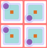
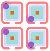
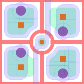

These are for the cell:
-
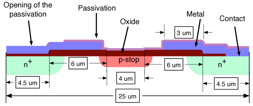
Figure 3: Cross section of the region between two pixels (marked as "cut 1" in Fig. 2(a)) for a sensor with no bias scheme (R4S100x25-P1). Horizontal dimensions are taken from the GDS file, vertical dimensions are only indicative. -
a)
Sensor with no bias scheme (R4S100x25-P1). The cross section along the direction, together with the relevant dimensions of the design, is shown in Fig. 3. The width of the implant is , the width of the metal overlap is and the -stop implant has a width of .
-
b)
Sensor with common punch-through for simultaneous biasing of four pixels and a straight bias rail (R4S100x25-P2). The bias dot has a diameter of , which is necessary to form the contact hole within the production tolerance. The total diameter, including the surrounding -stop implant, is . To reduce the losses along the bias rail, the -stop implantation underneath is wider than the metallisation of the rail [17].
-
c)
Sensor with bump bond pad in the middle of two pixels on top of the -stop implant. This is used for routing tests (R4S100x25-P4).
-
d)
Sensor with a wider implant (R4S100x25-P7). The width is and the metal overlap , resulting in a minimal distance between the metal plates of .
For the cell the designs are:
-
e)
Sensor with no bias scheme (R4S50x50-P1). The implant is wide.
-
f)
An open -stop design with an implant width of (R4S50x50-P2).
-
g)
Sensor with common punch-through for simultaneous biasing of four pixels and a straight bias rail (R4S50x50-P3). The implant size is . The bias dot and the bias rail are the same as for R4S100x25-P2.
-
h)
Sensor with common punch-through and a wiggle bias rail to prevent an overlap with the -stop implant. The implant size is .
In addition, sensors with bias dot, without a gap between the -dots and the surrounding -stop implant and sensors with polysilicon resistors have been designed for the ROC4Sens chip. The non-irradiated sensors with polysilicon functioned electrically, but exhibited problems in the test beam measurements, due to a too low resistance of the resistors. This manifested itself in a pattern in the hit map with a central band of pixels with signals and a cluster charge too small by a factor of two. Therefore, they are not considered as an option in the following.
2.2.2 Sensor designs for the RD53A chip
The RD53A chip is a prototype chip developed by the RD53 Collaboration with a non-staggered bump bond pattern of and 192 400 cells. The non-staggered bump bond pattern makes it necessary, in case of the pixel size, to implement a metal routing connecting the implant to the bump. Such routing on the sensor may result in additional cross talk between adjacent pixels. This issue needs to be further investigated with the RD53A readout chip.
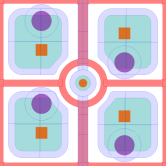
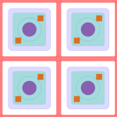
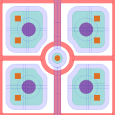
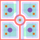
Twenty sensors (ten variants) for the RD53A chip are placed on a wafer. Of these, eight sensors have a cell and twelve sensors have a cell. For the -stop mask, the mask layout of the most promising designs are shown in Fig. 4. The dimensions of the implants, -stop implant and bias dots are the same as for the design for the readout with the ROC4Sens chip.




2.2.3 Guard ring
All sensitive sensor areas are surrounded by a guard-ring structure (Fig. 5) consisting of an inner or bias ring (in case of a bias structure), an outer ring and an edge ring. The inner and outer rings have openings in the passivation to allow for probing with needles.
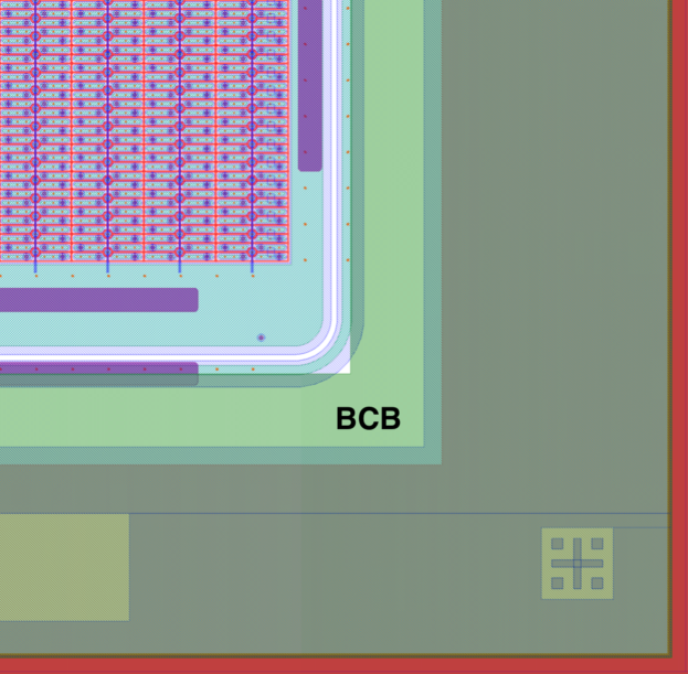
In addition, there are passivation openings for bumps on each side of the bottom of the inner ring that can be connected to the readout chip. This allows the inner ring to be either set to ground or left floating. In the case of a sensor without bias structure, grounding the inner ring should result in less noisy edge pixels, since the current from the inactive area is drained through this ring. The RD53A chip has the possibility of switching between both states by a jumper on the readout card, whereas this option is not available with the ROC4Sens chip. In this case, the UBM (Under Bump Metallisation) mask defines if the inner ring is grounded or left floating. The following measurements with the ROC4Sens chip are performed with the inner ring grounded, while for the measurements with the RD53A chip the inner ring was left floating.
2.3 Electrical measurements & yield
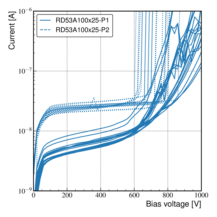
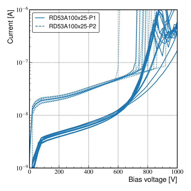
For an R&D production with new sensors, it is difficult to define meaningful acceptance criteria for the wafer. Therefore, sensor designs already successfully used during CMS’ HPK campaign [12] and pad diodes were used for this production to facilitate the acceptance of the wafers. Current-voltage measurements were performed by HPK on all sensors and diodes on the bias ring and inner guard ring, respectively. The measurements were done in steps up to . All delivered wafers met the requirements in terms of full depletion voltage, leakage current and breakdown voltage as specified in Table 1. In general the results indicated a high fraction of acceptable sensors with high breakdown voltage (> ) for the different sensor designs, but also revealed some problematic combinations of sensor design and material. For example, on the FDB150 wafers with -stop isolation the sensors of type R4S100x25-P2 have a yield of only 25%, while they have a yield of 100% on the FTH150 and FDD150 wafers. It is also observed that the leakage current on the FDD150 wafers is a factor of 10 larger compared to the FTH150 and FDB150 wafers, and it varies significantly across a wafer. As a consequence, sensors on FDD150 wafers with bias structure cannot be distinguished from sensors without bias structure based on – measurements. This is in contrast to the case on FTH150 and FDB150 wafers, whose – curves are shown in Fig. 6, and complicates the determination of good FDD150 sensors using the – measurements.
The reason for the high leakage current of sensors from FDD150 wafers is probably a deep hole trap with the designation , which was found using deep-level transient spectroscopy on similarly processed test structures [13] and is known as a possible current generator. In addition, a very high oxygen concentration and a thickness dependence of the defect concentration were found. From this it can be concluded that the defects were formed during the deep-diffusion process.
Capacitance-voltage (–) measurements on diodes of different sizes were performed to determine the full depletion voltages and doping profiles taking edge effects into account [18]. The full depletion voltage is in the range of 55 to , depending on the substrate. Examples of doping profiles of the different substrates are shown in Fig. 7, indicating that the active thickness of FTH150 and FDB150 sensors is close to the specified .
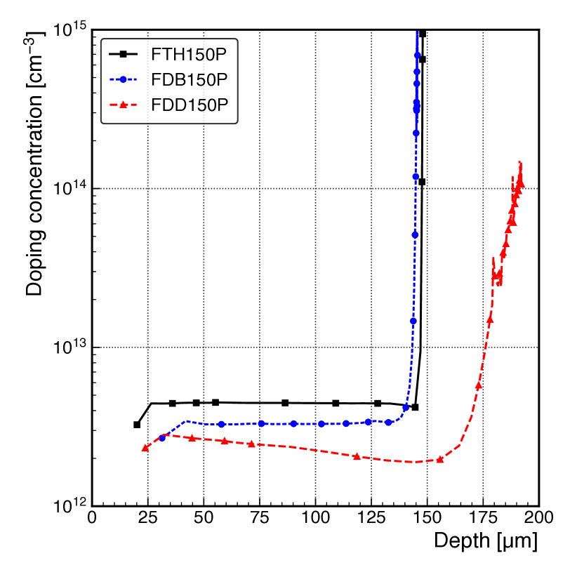
The bulk doping concentration of FTH150 sensors is around , while it is for FDB150 sensors. The doping profile of the deep diffused substrate is very inhomogeneous in the sensitive region of the sensor and the active thickness is larger than . As a result, this material is excluded from further consideration.
3 Sample preparation
3.1 Readout chips
Both types of readout chips, the ROC4Sens chip and the RD53A chip, were used to characterise the HPK sensors.
The ROC4Sens chip is based on the PSI46 chip (fabricated in the same IBM process) and is intended for sensor studies only. The chip has pixels and a total size of . The chip is easy to operate and can be read out with the same Digital Testboard (DTB) as used for the testing of the CMS Phase-1 pixel readout chips [19] after adapting the firmware, adapter and software. There are no DACs to be set, only two shift registers to be programmed, no discriminator threshold adjustment or trimming needed and only a small number of control signals is required. The signal processing of each pixel features a pre-amplifier and a shaper with fast pulse shaping. The collected charge can be stored on a sample-and-hold capacitor. When the charge of a hit is being stored, the pixel cannot accept further incoming hits. As there is no internal signal on the chip or pixel which indicates a hit, the storage and readout of a hit has to be triggered externally with the trigger signal distributed to all pixels simultaneously. With digitisation of all pixels with resolution in the DTB this allows for data taking without zero suppression at rates of around . To save disk space only regions of interest, pixels centred around a seed pixel with a charge above threshold, are stored.
The RD53A chip [4] is a prototype for the ATLAS and CMS readout chips planned for operation at the HL-LHC. The chip has three analogue front-end flavours. Only the linear front-end, which covers 1/3 of the entire pixel matrix and which is the front-end selected by CMS [20], is used in this study. It provides a self-triggering mode, which facilitates source scans to be performed, and stores the charge using the time-over-threshold method with accuracy. For non-irradiated chips a threshold 1000 electrons is achieved.
3.2 Flip chip & spark protection
Under-bump metallisation on the sensor wafer, bump deposition on the chip wafer and flip-chip bonding of single-chip ROC4Sens and RD53A modules were done at Fraunhofer IZM [21]. The technology chosen uses SnAg bumps on the readout chip and Ni-Cu pads on the sensor. The chips for the studies of this paper were thick. In case of the ROC4Sens modules, the bump-bond yield was usually above 99.5%.
To prevent sparking between sensor and chip at high bias voltage the option to use a benzocyclobutene (BCB) frame on the sensor [22] has been investigated. The BCB was deposited as a frame from the cut edge to the bias ring on the sensor, as shown in Fig. 5. However, measurements carried out on non-irradiated modules in the laboratory showed sparking at a voltage of , requiring alternative solutions. For the test beam measurements, it was found that a protection of the modules with SYLGARD 184 Silicone Elastomer [23] was sufficient to safely operate the modules up to without sparking. SYLGARD is not a practical option for the module production of the final detector, but we do not expect its usage to affect the results obtained in this paper.
3.3 Irradiations
At the radial position of the pixel sensors the fluence is dominated by charged hadrons, therefore those should be used in irradiation studies. Unfortunately, for higher proton fluences the shaping time in the ROC4Sens chip cannot be configured as needed. To achieve fluences above , the modules were irradiated with neutrons. Even though the electrical fields and trapping times are different after proton and neutron irradiations [24], it was shown in Ref. [25] that the collected charge in - sensors is similar.
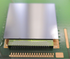
Before proton irradiation most of the modules were first glued to a printed circuit board (PCB), wire bonded and tested for basic functionality. An example module is shown in Fig. 8.
For neutron irradiation, untested bare modules were put into 3D-printed boxes, and irradiated before wire bonding.
A list of all samples used in the following studies is given in Table 3.
The neutron irradiation was performed in the TRIGA Mark II reactor in Ljubljana. The neutron equivalent fluences were 0.5, 3.6, 7.2 and , determined using a hardness factor of 0.9 [26].
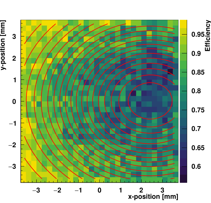
The proton irradiation was performed at the PS-IRRAD Proton Facility at CERN (PS) with a beam momentum of to fluences of 2.0 and averaged over the sensors. The hardness factor used in the following calculation is 0.62 [27]. All samples were not biased during irradiation and kept at room temperature. Contrary to the neutron irradiation, the proton irradiation was non-uniform with an approximately Gaussian beam profile with a FWHM between 12.5 and . In addition to the aluminum foils for dosimetry, several beam position monitors (BPMs) were installed in the IRRAD facility, which can be used to reconstruct the beam profile in horizontal and vertical direction orthogonal to the beam. Using this information and the aluminum foils for normalisation the total delivered proton fluence and the fluence profile for the modules can be estimated. For correct positioning of the profile with respect to the module, the position of the minimum in hit efficiency is set equal to the position of maximum fluence. An example is shown in Fig. 9. The fluences in the beam spot area are about and , the respective numbers are quoted in the legends of Figs. 16-19. For the sensors bump bonded to the ROC4Sens readout chip, the fluences, efficiencies, and signal-to-noise ratios are quoted for a circular region with radius around the point of highest irradiation. The uncertainties on the fluences are estimated to be 17%.
For the sensors bump bonded to the RD53A readout chip, the fluences are averaged over the area of the sensor read out by the linear front-end, which is about .
Except for the irradiation, transport and handling, the sensors are stored at to avoid annealing. The integrated annealing of these steps accounts to 2-3 days at room temperature, and it is not comparable to planned annealing steps in the detector, usually 2-4 weeks long.
3.4 I-V after irradiation
The leakage current as a function of the bias voltage was measured during the beam test and in the lab. Figure 10 shows the – curves of different ROC4Sens modules irradiated with neutrons or protons, measured at .
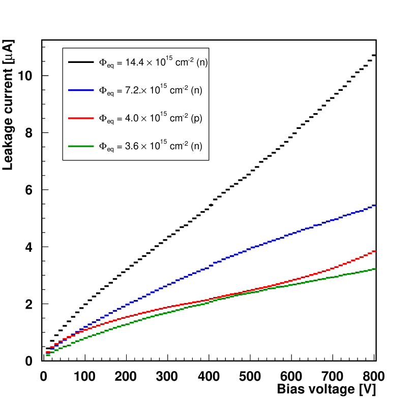
As expected, the leakage current increased with fluence. However, as none of the – curves shows saturation it is questionable how to extract the current-related damage factor [7]. Therefore, we refrain from presenting values of this parameter, instead we discuss values of current at a fixed voltage.
For the lowest fluence the – curve of the sample irradiated with neutrons is in good agreement with the – curve of the sample irradiated with protons, which shows that the non-ionizing energy loss scaling for the current applies. The NIEL hypothesis assumes that radiation damage effects scale linearly with NIEL irrespective of the distribution of the primary displacements over energy and space [7]. To estimate the power dissipation at a temperature of the current can be scaled using with the activation energy and being the Boltzmann constant [28]. For a fluence of the leakage current is expected to be at and the dissipated power is expected to be . It should be noted that this leakage current value is higher compared to the requirement in Table 1, but it is obtained for a fluence much higher than specified.
4 Beam test setup
The beam test measurements were performed at the DESY II test beam facility [29] in the period 2017-2019. DESY II provides an electron beam with momenta between 1 and , which is generated via a two-fold conversion and with momentum selection by a spectrometer dipole magnet. For the following measurements a beam momentum of was used.
4.1 Beam telescope
The EUDET DATURA beam telescope [30] installed in the beam line TB21 was used. The telescope consists of six planes, each equipped with MAPS-type MIMOSA26 sensors which have a pixel size of and are thinned down to a physical thickness of . As shown in Fig. 11 the planes are separated into three-plane triplets upstream and downstream with respect to the position of the device under test (DUT).
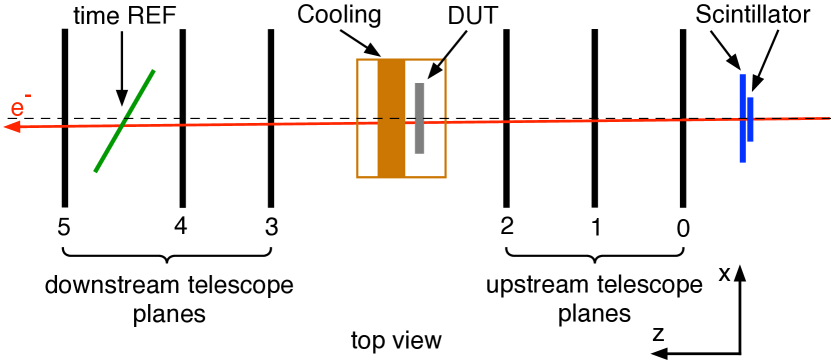
Operating the MIMOSA26 planes with threshold set six times the RMS noise an intrinsic hit resolution of a single plane of can be achieved. Due to the long integration time of for the MIMOSA26 planes, tracks in-time with the readout cycle of the DUT are selected with a CMS Phase-1 pixel module [19], serving as time reference plane with a time tagging capability of . Trigger scintillators upstream of the beam telescope provide a trigger signal for the telescope, the CMS Phase-1 pixel module and the DUT.
4.2 Pixel sensor assembly and cooling
The pixel sensor assembly and cooling are similar to those already used for previous CMS Phase-1 test beam measurements [31]. The investigated pixel module is glued on a PCB carrier board with edge connectors. This carrier board is attached to a readout card mounted on a copper plate and connected to the readout electronics. To reduce the material in the beam, the copper plate has a cut-out around the position of the DUT. Inside the plate, the coolant liquid from an ethanol-based chiller circulates through a cooling loop to control the temperature of the DUT. In addition, two Peltier elements operating at 5 to in direct contact with the PCB holding the DUT are used to improve the cooling. For thermal insulation and to prevent condensation, the copper support structure is placed in a plastic box, referred to as cold box, wrapped with ArmaFlex insulation and flushed with dry air. The cold box is mounted on a set of two translation stages and one rotation stage, which allows remotely controlled movements in the and -directions (orthogonal to the beam axis) and rotation around one axis of choice.
To limit the leakage current for the irradiated sensors, the modules are cooled to for the setup with the ROC4Sens modules and for the setup with the RD53A readout chip. The small difference is due to different thermal connections in the two cooling boxes used. Cold operation is especially important for the ROC4Sens modules since this chip has no leakage-current compensation and it has been found that already a leakage current of per pixel is sufficient to significantly reduce the resistance of the feedback transistor of the preamplifier [5].
4.3 Sensor readout and data acquisition
A coincidence trigger is generated from the signals of two scintillators, read out by photomultiplier tubes (PMTs). To define an acceptance window slightly bigger than the active region of the ROC4Sens module, two trigger scintillators in a cross configuration are placed upstream of the beam telescope. The output signals of the two PMTs are passed to the trigger logic unit (TLU). The TLU is configured to send out a NIM level trigger signal on a coincidence of the two scintillator signals. This trigger signal is fed to a NIM discriminator to suppress occasional double pulses by choosing a sufficiently long gate. The discriminated signal is converted to TTL standard, split using a fanout and passed to the DTBs for the DUT and the time reference plane. To optimise the efficiency of the time reference plane, its trigger signal needs an additional delay of several nanoseconds. The internal delays of the electronic devices on the trigger line accumulate to about . The total delay including cables corresponds to approximately . Therefore the pulse shape of the single pixels in the ROC4Sens modules is delayed to peak around the latter value.
5 Data analysis
In the following, only the data analysis for beam tests with the ROC4Sens modules as DUT is described in detail. Only one result with RD53A readout is included, and merely for completeness. A description of the tuning procedure for the RD53A readout chip is beyond the scope of this paper.
5.1 Online analysis
As the ROC4Sens chip has no zero suppression, all pixels are read out for each event by the DTB and the digitised response is sent to a PC. To reduce the amount of stored data, only the information of possibly hit pixels and pixels from a region of interest (ROI) around them is stored. This is done by applying the following procedure [32]:
-
1.
Pedestal correction for each pixel: the pedestal is first calculated as the average response of a pixel using the first 200 events of a run. Subsequently, it is updated as running average.
-
2.
Correction for baseline oscillations common to all pixels (common-mode correction): for this the differential pulse height, , defined as
(1) where is the pedestal corrected pulse height, measured in ADC counts, of the pixel with column and row indices and , respectively, is used. This correction can be applied in a column-wise or row-wise sequence. Both procedures were used for the later measurements.
-
3.
Finally, to select hits the time-dependent quantity (significance)
(2) is introduced as discriminator. Using a threshold a pixel , is marked as hit if:
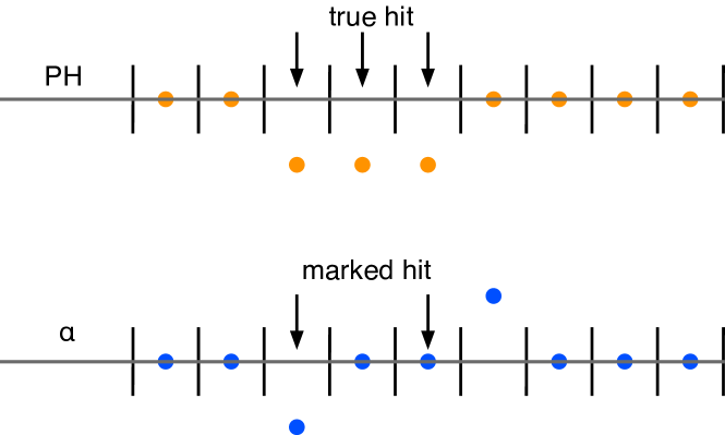
(3) The usage of instead of is advantageous, as effects of gain variations are mitigated and noisy pixels are automatically suppressed. The two conditions are needed to deal with clusters of hit pixels, especially if several consecutively read out pixels are hit. Figure 12 shows schematically a hit pattern of three hit pixels in and . It is clear that the conditions of Eq. 3 identify the leading and trailing hit of a cluster.
-
4.
The pulse heights are stored for a region of interest, which consists of pixels centered around a hit pixel.
As a compromise between efficiency of the hit identification, purity of the data sample and required disk space, all measurements were performed with .
For the six MIMOSA26 sensors, the threshold is applied on the chip and only the positions of the pixels exceeding the threshold are stored (binary readout). A threshold of 5 or 6 times the individual pixel noise is used.
For the CMS Phase-1 module used as time reference (time REF), the response of pixels above a threshold of 1500 e- is digitised with 8 bit precision and stored together with the pixel positions.
5.2 Offline reconstruction and alignment
A fast and flexible custom reconstruction and analysis software is used. The reconstruction is performed in two steps. In the first step the reference tracks of the telescope are reconstructed and the telescope planes are aligned. In the second step the reference tracks are matched to the DUT and to the time reference module. Their projected track positions are matched to hits on those modules and their alignment is determined. In both steps, an iterative approach is used, starting with loose cuts, still leaving a lot of combinatorial background, and iteratively using tighter cuts, resulting in a more precise alignment.
The alignment of the telescope starts with the readout of the binary pixel hit information from the MIMOSA26 sensors, where noisy pixels are detected and removed from further analysis. Afterwards, a topological cluster algorithm is applied, which combines adjacent hit pixels into a cluster and calculates its position in local coordinates as a weighted sum of the pixel positions with the number of neighbouring hit pixels as weights. Fixing the position of plane 1 for the upstream arm and plane 4 for the downstream arm of the telescope allows the calculation of cluster correlation histograms and profiles between the planes 0 and 2 with plane 1 and planes 3 and 5 with plane 4 to determine relative shifts in , and rotations around the -axis.
Next, a triplet method is applied separately to the upstream and downstream arm to find initial track candidates. In case of the upstream arm, for all possible hits in plane 0 straight lines connecting to all possible hits in plane 3 are formed. To reduce the number of combinations, track candidates with an absolute slope greater than are rejected. Remaining tracks are rejected, if no matching hit is found in plane 1 within in and of the interpolated line. The track candidates for the downstream arm are calculated using the same method. The slope of the upstream and downstream triplets is used to align the -position of planes 2 and 5. Finally the upstream and downstream triplets are extrapolated to the nominal -position of the DUT and correlated to determine the relative alignment between the upstream and downstream triplets. Only tracks for which the residuals of the and positions at the DUT between the two extrapolated triplets are smaller than are considered for the alignment.
The second step starts with the reconstruction of the hits in the DUT and the time REF. For the DUT pixel ROIs, which might overlap, are read out and a fixed threshold , whose value is optimised for the spatial resolution of each individual module, is applied. For non-irradiated modules, the response is corrected for gain variations, non-linearity, common-mode and cross talk, whereas for irradiated modules, due to the radiation effects on the calibration circuit, only common-mode and cross talk is corrected. For the DUT and the time reference plane, the same clustering algorithm as in Ref. [31] is applied. Starting with a seed pixel the number of hits in the cluster is obtained by adding neighbouring pixels that are above the threshold and adjacent to a pixel of the cluster. A new seed pixel is selected if there are still pixels above threshold after removing the pixels of the cluster. The cluster position is calculated with the Center-of-Gravity algorithm.
The alignment of the DUT and the time reference plane is carried out in a similar way as the alignment of the telescope. For the DUT, the residuals of the - and -coordinates are the difference between the cluster position reconstructed in the DUT and the average of the positions obtained by extrapolation from upstream triplet tracks and downstream triplet tracks to their intersection with the DUT plane. Small differences between upstream and downstream extrapolation are to be expected due to multiple scattering in the material traversed by the electrons. The extrapolated values are calculated from the intersection points between track and DUT, taking into account the -position and orientation of the DUT. Then the intersection points are transformed into local DUT coordinates and the alignment parameters are determined as for the telescope, taking into account rotations around the and axis in addition. In case of the time reference plane, only the downstream triplet tracks are considered for the alignment.
5.3 Event selection and definition of observables
For the determination of the properties of the DUT, the tracks have to fulfil additional requirements:
-
1.
Residuals in and between the interception points of the extrapolated upstream and downstream triplet at the DUT must be .
-
2.
For each extrapolated downstream triplet at the time reference plane the distance to the nearest other triplet must be .
-
3.
Residuals in and between the track intersections and the cluster positions in the time reference plane must be . Such tracks are considered as in time with the DUT.
-
4.
The tracks have to be inside of the sensitive area of the DUT (fiducial cuts).
-
5.
A time difference of between events recorded by the DUT and TLU is required to assure synchronization between them.
5.3.1 Hit detection efficiency
The hit detection efficiency and its error are defined as
| (4) |
where denotes the number of in-time telescope tracks and the subset of those tracks matched with a hit in the DUT. A hit is defined as a pixel fulfilling the conditions in Eq. 3 with . This threshold is the same as the online threshold and this definition ensures an approximately constant noise rate for all samples and conditions. To match a track with a DUT hit, the hit must be within a radius of of the track. For modules irradiated non-uniformly with protons, the efficiency is averaged over the beam spot area.
5.3.2 Charge
For each of the tracks the charge of the cluster with the largest cluster charge within a radius of around the track is stored. The signal is determined as the most probable value (MPV) of a Moyal distribution [33], with two free parameters, MPV and width, fitted to the cluster charge distribution. The Moyal function is chosen for single pixel distribution fits instead of a Landau distribution, due to its higher robustness in fits with low statistics.
5.3.3 Noise
The noise of each pixel is defined by the RMS of its response in the absence of particles. It defines the individual threshold of each pixel, as discussed above. To calculate the signal-to-noise ratio, the noise is averaged over all pixels inside the area (e.g. an area of radius for ROC4Sens modules irradiated with protons) considered for the determination of the efficiency and the signal.
5.3.4 Spatial resolution
To reduce non-Gaussian tails in the residual distribution the selection for the determination of the spatial resolution is more elaborate. A fixed threshold optimised for the resolution at the angle with the best resolution is used. In addition the track is required to be isolated at the DUT. This is ensured by requiring a minimum distance of the upstream triplet track extrapolated to the DUT to the nearest other triplet track of . If there are ambiguous combinations of hits and tracks, only the closest pairs are considered. In addition, there is a cut on the DUT residuals (Eq. 5) orthogonal to the investigated direction, which depends on the sensor pitch (it is for the sensors), and finally a charge cut where the events with the 10% highest charge are rejected to remove delta-electrons.
The resolution in the -direction (similarly for the -direction) is extracted from the distribution of the DUT residuals, , defined as
| (5) |
where denotes the position of a DUT cluster and the point of intersection of a telescope track in DUT coordinates, as discussed in Section 5.2. To determine the width of this distribution, a method which respects the non-Gaussian nature of the distribution for angles close to and which is stable with respect to outliers, a truncated RMS denoted as , is used. The calculation of the truncated RMS is performed iteratively by discarding values outside of . A similar approach is applied to residuals of the telescope, where
| (6) |
with being the -coordinate of the extrapolation of the upstream triplet to the -position of the DUT and defined similarly for the downstream triplet. The effective telescope resolution, defined as the uncertainty of , is given by
| (7) |
where is the rotation angle of the DUT around the -axis. The factor 2 in the denominator results from averaging the position prediction of upstream and downstream telescope tracks, assuming that the uncertainty of these is the same. Once the effective telescope resolution is known, the resolution of the DUT is
| (8) |
6 Results
6.1 Results for non-irradiated modules
Different non-irradiated types of pixel modules were investigated in the test beam to compare their performance to expectations and to identify less promising designs. As mentioned above, several sensor designs with polysilicon resistors showed problems already at this stage, which led to their exclusion from the further test program.
In Fig. 13 a typical cluster charge distribution together with a fit using a Landau distribution convolved with a Gaussian distribution is presented. The data are from a module with a sensor design R4S50x50-P1 which has a pixel size of and is from a FTH150 wafer.
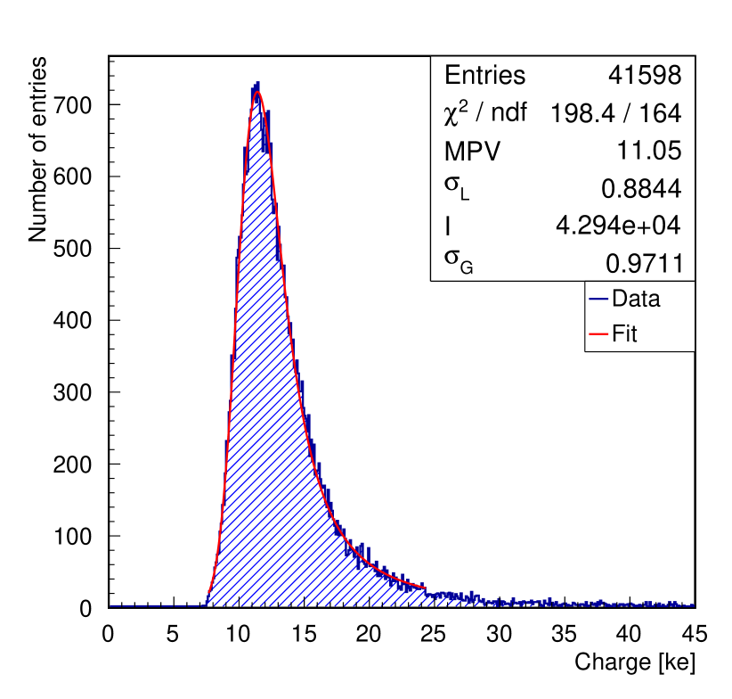
The sensor was biased at . The measurement was done at a beam energy of 5.2 GeV with normal beam incidence. For the absolute charge calibration, a gain calibration (pulse height vs. internal charge injection pulse for every pixel) was performed and the charge was scaled by a factor of 24.3 ADC counts/ke- so that the most probable value is e-, which is the expected value from simulations for a sensor with thickness.
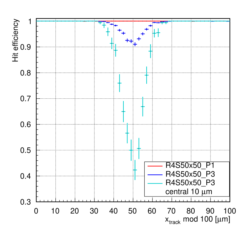
For the non-irradiated pixel modules at a bias voltage of the hit detection efficiency is typically well above 99%, with the exception of the designs with bias dot. Significant efficiency losses are observed at the bias dot position as shown in Fig. 14, where the projected hit efficiency as a function of the in-pixel position is plotted for a module without bias scheme (R4S50x50-P1) and a module with common punch-through and straight bias rail (R4S50x50-P3). For the sensor with bias dot, the projected hit efficiency drops to 92%. The drop in a region in the center of the bias dot is even more severe; here the efficiency is reduced to 40%, as shown by the cyan curve.
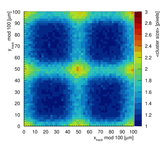
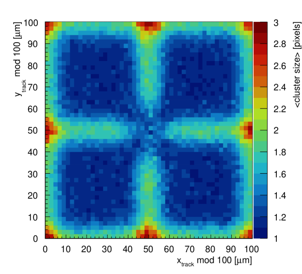
The reduction of performance due to introduction of a bias dot is also evident from the comparison of the mean cluster size as function of the in-pixel position of sensors with and without bias dot, as shown in Fig. 15. In Fig. 15(a) the case without bias scheme and in Fig. 15(b) the case with common punch-through and straight bias rail is presented. In both cases the pixel size is . The bias dot, which is in the centre, introduces a reduction of the cluster size.
6.2 Hit detection efficiency
To quantify the hit detection efficiency, defined in Sec. 5.3.1, as a function of fluence, measurements were performed with normal beam incidence for voltages up to . First, results after neutron irradiation with fluences of 0.5, 3.6, 7.2 and are discussed. The investigated sensors are read out with the ROC4Sens readout chip. The sensors feature a pixel size of and a -stop pixel isolation technology, as favoured by HPK. The pixel cell designs are without bias structure. Presented are the results of R4S100x25-P1 shown in Fig. 2(a) for the three sensors irradiated to the lower fluences, and the design R4S100x25-P7 with enlarged implants shown in Fig. 2(d) for the sensor irradiated to the highest fluence.
In Fig. 16 the hit detection efficiency measured for the four sensors is shown as a function of the applied bias voltage.
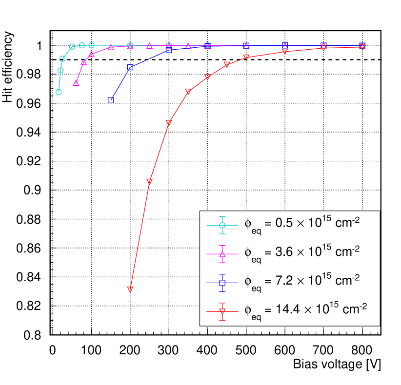
The required bias voltages for an efficiency of 99%, indicated as dashed horizontal line, are about 25, 85, 250 and from the lowest to the highest fluence, respectively. In general, the reason for the reduction of the hit efficiency with increasing fluence is two-fold: due to trapping of charge carriers the signal decreases with increasing fluence, while the noise increases with fluence. In addition, the electric field changes, with the region of high fields becoming smaller as the fluence increases.
The value of for a fluence of can be compared to the full depletion voltage of below before irradiation. For the highest fluence , the value of is well below the specified . However, even though there appears only little difference in the amount of collected charge in strip sensors after neutron- and proton irradiation, as shown in Ref. [34], such a conclusion must be taken with caution.
In Fig. 17(a) the signal-to-threshold ratio measured for the four sensors is shown as a function of the applied bias voltage.
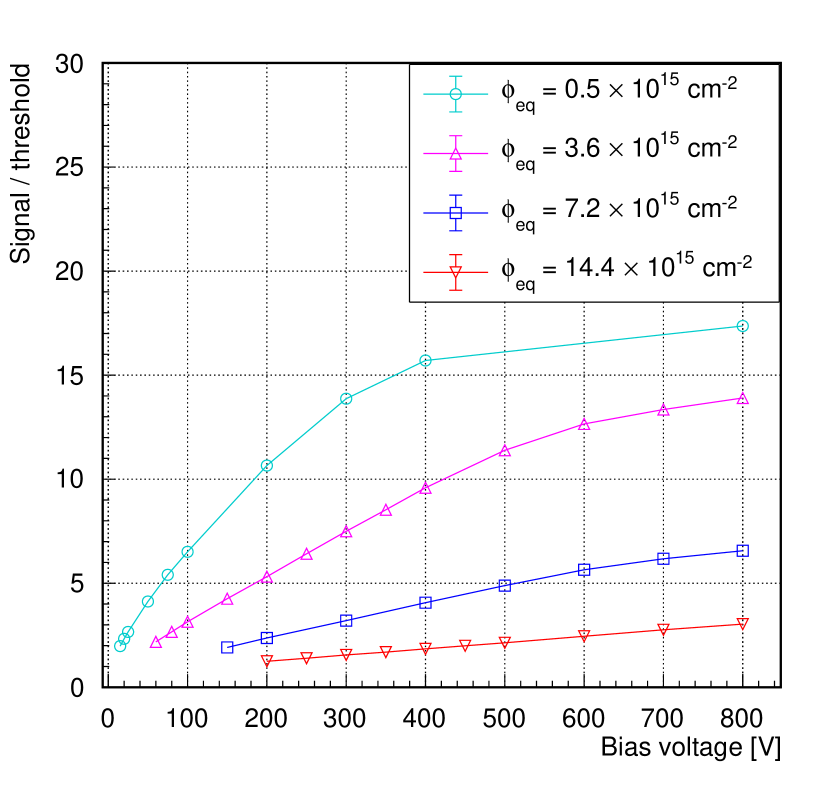
The threshold is chosen as four times the noise — therefore the noise rate stays constant — to ensure a fair comparison between the measurements taken under different conditions. The noise as a function of bias voltage is constant to within 5%, while it doubles from the lowest to the highest fluence. However the variation shown in the figure is by far dominated by the reduction of the signal, caused by the reduction of collected charge.
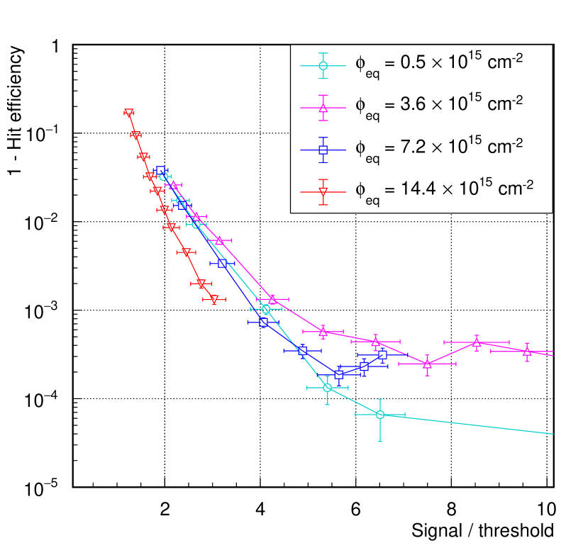
Figure 17(b) shows the inefficiency as a function of the signal-to-threshold ratio. Independently of the fluence, the three sensors of type R4S100x25-P1 reach an inefficiency of 1% at a signal-to-threshold ratio of about 2.6. This inefficiency is reached at a signal-to-threshold value of 2 in the case of the highest fluence. This is related to the larger implant of the sensor of type R4S100x25-P7, as will be shown below.
The mechanisms of neutron and proton radiation damage are known to differ at the microscopic level [35]. In the following, an attempt is made to quantify the different impacts on the performance of the sensors.
The efficiency as a function of the bias voltage for two sensors irradiated with protons to 5.2 and is shown in Fig. 18.
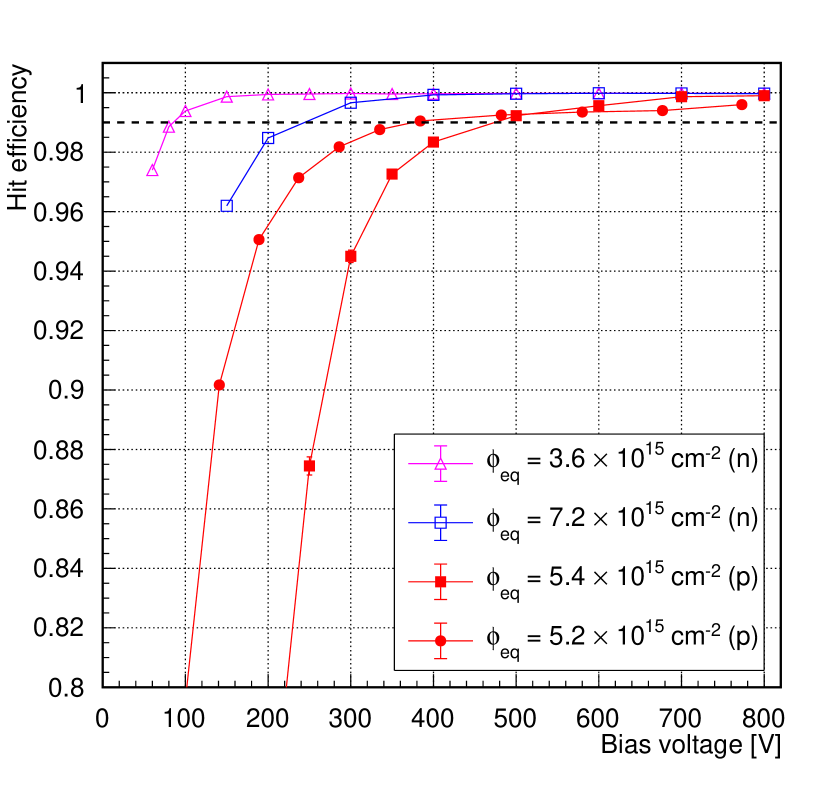
For comparison, the two intermediate neutron fluences from Fig. 16 are included. It is concluded that the modules irradiated with protons require significantly higher operating voltages than those irradiated with neutrons for an efficiency of 99%, for which there are two reasons. One is the higher (factor of 30) ionising dose deposited by the proton beam. Since the ROC4Sens readout chip is more sensitive to ionising radiation, the steep rise to about 95% occurs at higher bias voltages222The module with the RD53A readout chip has lower efficiency due to 0.5% of dead pixels, which have not been excluded from the analysis.. The second reason is the difference in bulk damage, which is investigated in Ref. [36] for neutron and pion irradiation.
These measurements show that the tested sensors reach an efficiency of 99% for bias voltages significantly below for a fluence of .
6.3 Sensor Design Comparisons
To choose the optimal sensor layout for the upgraded detector, modules with different sensor designs are compared after irradiation.
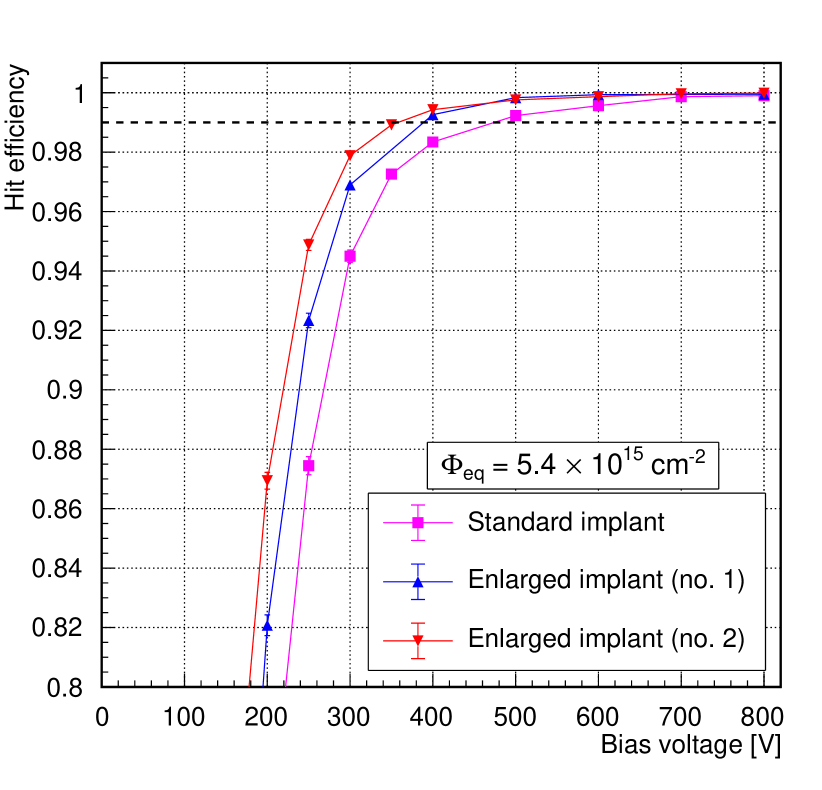
Wider implants are expected to yield higher hit efficiencies [37]. However, the risk of breakdown before irradiation is increased, due to the potentially higher field at the -stop isolation. Current-voltage measurements were performed on about 70 sensors with enlarged implants, and no evidence of breakdown was observed. In Fig. 19 a comparison of the hit efficiency of two sensors with and one sensor without enlarged implant is shown. Indeed a higher hit efficiency is observed for the design with wider implants at the same bias voltage.
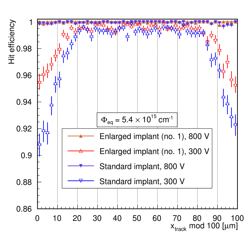
As shown in Fig. 20, this is due to reduced efficiency losses at the pixel boundaries.
Given the excellent performance of the designs with enlarged pixel implants, this design will be further tested in the next prototyping steps.
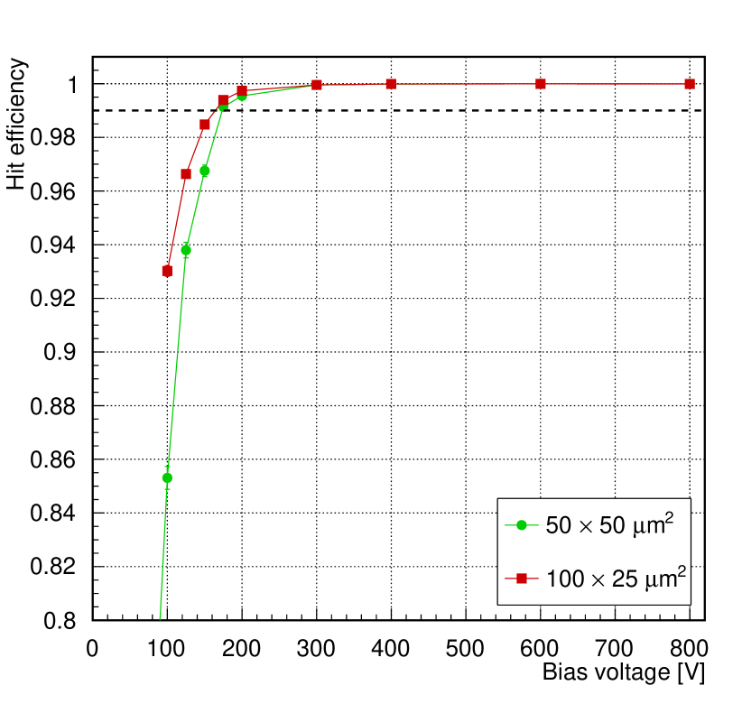
The comparison of sensors with pixel sizes of and shown in Fig. 21 shows only minor differences.
6.4 Charge losses at the bias dot
For sensors with a bias dot, charge losses are expected when tracks hit the bias dot with an angle almost perpendicular to the sensor plane. To assess these losses in detail, the efficiency as a function of the position in the pixel is shown in Fig. 22 for angles between 0 and . The investigated sensor is read out by an RD53A readout chip and was irradiated with protons to a fluence of . The sensor is of type RD53A100x25-P2, shown in Fig. 4(b).
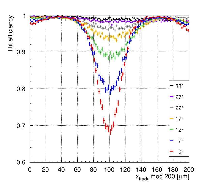
It is observed that angles larger than are needed to overcome the efficiency loss at the bias dot, which is as high as 30% for . Since angles close to are expected to be frequent in the forward pixel detector, the design without a bias dot is clearly favoured.
6.5 Spatial resolution
Detailed studies of the spatial resolution after irradiation have been performed with the DATURA telescope only for sensors with a pixel size of . In the following, the measurements before irradiation and after neutron or proton irradiation are presented as a function of the beam incidence angle. Measurements of the non-irradiated sensor were made at , while the irradiated samples were measured at to maximise the collected charge. The reconstruction of the resolution and the event selection was done as described in Sec. 5.
Sensors irradiated with neutrons to fluences of and have been investigated. The studies include a non-irradiated sensor of R4S50x50-P8 type, which is with an enlarged implant and without bias structure, for comparison with the results after irradiation. The sensor irradiated with the higher fluence is of the R4S50x50-P1 type, while the sensor irradiated with the lower fluence is the corresponding -spray version. The spatial resolution in direction is studied as a function of the rotation angle around the -axis, . The analysis has been performed in two steps. In the first step the threshold is optimised at the angle with best resolution (optimal angle), which is for the lower fluence and for the higher fluence. This has to be compared to for a non-irradiated sensor. The optimal angle for the larger fluence is significantly higher. This is due to the fact that the depth dependence of the charge collection increasingly reduces the effective thickness of the pixel sensor with increasing fluence. The optimal threshold values are determined as 12, 18 and 20 ADC counts, respectively, from the lowest to the highest fluence. They correspond to signal-to-threshold values of 5%, 8% and 11% of the Landau MPV. In the second step the spatial resolution as function of the beam incidence angle is determined using these threshold values. In Fig. 23(a) the results are shown in comparison to those of the non-irradiated sensor.
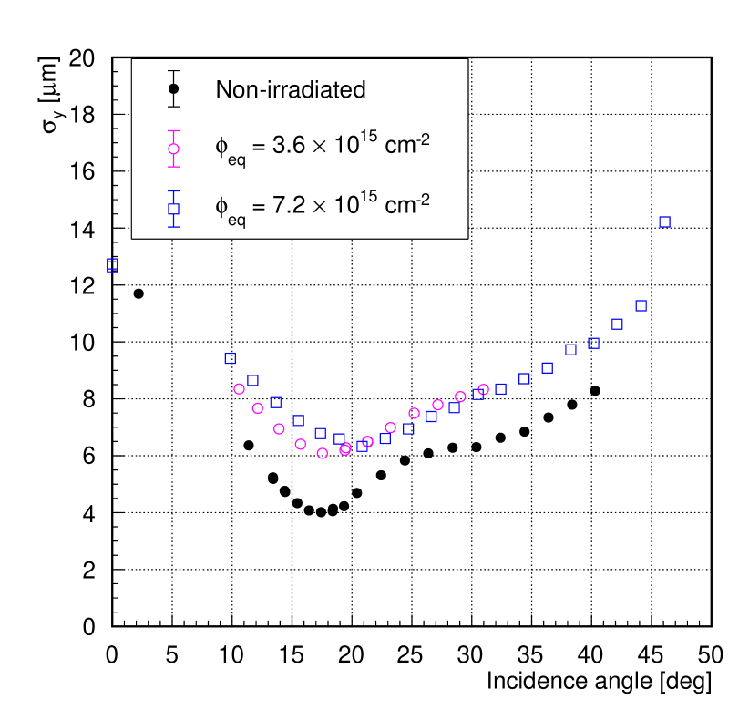
The shapes of the curves are qualitatively similar. However, the resolution at the optimal angle degrades from to after and to after .
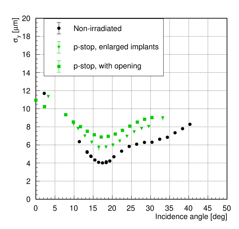
To study the resolution after proton irradiation, two samples of different type, irradiated with protons to nearly the same fluence of , were used. One is of type R4S50x50-P2, which has an open -stop isolation, and one of type R4S50x50-P8, which has an enlarged implant. As in the case of the neutron irradiation the measurements have been performed at . The threshold optimisation at the optimal angle results in 16 ADC counts for the sensor with enlarged implants and 18 ADC counts for the sensor with the open -stop isolation, which corresponds in both cases to 10% of the Landau MPV. In Fig. 23(b) the spatial resolution as a function of track angle determined with these threshold values is shown in comparison to the non-irradiated sensor. The resolution at the optimal angle degrades from to for the design with the enlarged pixel implant and to for the open -stop after .
7 Conclusions
This paper summarizes the qualification of planar pixel sensor designs suitable for the CMS Inner Tracker, investigated using an R&D chip (ROC4Sens). The results presented in this paper demonstrate that some of the designs implemented on an HPK submission reach efficiencies of 99% for minimum ionising particle tracks normal to the sensor plane at voltages above 500 and after neutron and proton irradiation to fluences of up to 14.4 and , respectively. The higher value is above the fluence expected for planar pixel sensors in the upgraded CMS Inner Tracker, which is about .
The intrinsic single plane resolution along the pitch direction is shown to be for the non-irradiated sample at the optimal angle, while it worsens to after neutron irradiation of .
The measurements presented in this paper have informed the choice of the sensor design, together with other studies such as physics performance simulations and thermal modelling. Planar sensors with a pixel size of will be used everywhere except in the innermost barrel layer, where 3D sensors with the same pixel size will be employed. The planar sensors will not feature a punch-through bias dot, but an enlarged implant. A cell design similar to that of Fig. 4(a) is going to be used. Parylene coating will be used for spark protection.
Further studies, including measurements at higher irradiation fluences that require a calibrated RD53A readout chip, are ongoing. Preliminary studies for angles up to were presented in Ref. [38].
Acknowledgements
This work was supported by the German Federal Ministry of Education and Research (BMBF) in the framework of the "FIS-Projekt - Fortführung des CMS-Experiments zum Einsatz am HL-LHC: Verbesserung des Spurdetektors für das Phase-2 Upgrade des CMS-Experiments" and supported by the H2020 project AIDA-2020, GA no. 654168. The measurements leading to these results have been performed at the Test Beam Facility at DESY Hamburg (Germany), a member of the Helmholtz Association (HGF).
The tracker groups gratefully acknowledge financial support from the following funding agencies: BMWFW and FWF (Austria); FNRS and FWO (Belgium); CERN; MSE and CSF (Croatia); Academy of Finland, MEC, and HIP (Finland); CEA and CNRS/IN2P3 (France); BMBF, DFG, and HGF (Germany); GSRT (Greece); NKFIA K124850, and Bolyai Fellowship of the Hungarian Academy of Sciences (Hungary); DAE and DST (India); INFN (Italy); PAEC (Pakistan); SEIDI, CPAN, PCTI and FEDER (Spain); Swiss Funding Agencies (Switzerland); MST (Taipei); STFC (United Kingdom); DOE and NSF (U.S.A.). This project has received funding from the European Union’s Horizon 2020 research and innovation programme under the Marie Skłodowska-Curie grant agreement No 884104 (PSI-FELLOW-III-3i). Individuals have received support from HFRI (Greece).
References
- O. Brüning and L. Rossi [2019] O. Brüning and L. Rossi, The High-Luminosity Large Hadron Collider, Nat. Rev. Phys. 1 (2019) 241–243. doi:10.1038/s42254-019-0050-6.
- CMS Collaboration [2017] CMS Collaboration, The Phase-2 Upgrade of the CMS Tracker, Technical Report CERN-LHCC-2017-009, CMS-TDR-014, 2017. URL: https://cds.cern.ch/record/2272264.
- Taiwan Semiconductor Manufacturing Company Limited (2017) [TSMC] Taiwan Semiconductor Manufacturing Company Limited (TSMC), 2017, URL: https://www.tsmc.com/.
- RD53 Collaboration [2015] RD53 Collaboration, RD53A Integrated Circuit Specifications, Technical Report CERN-RD53-PUB-15-001, 2015. URL: https://cds.cern.ch/record/2113263.
- Wiederkehr [2018] S. Wiederkehr, The Effective Lifetime of and Designing a Readout Chip for Pixel Sensor Development, Ph.D. thesis, ETH Zürich, 2018. doi:10.3929/ethz-b-000314130.
- R. Klanner et al. [2020] R. Klanner et al., Determination of the electric field in highly-irradiated silicon sensors using edge-TCT measurements, Nucl. Instrum. Methods Phys. Res. A 951 (2020) 162987. doi:10.1016/j.nima.2019.162987.
- Moll [2018] M. Moll, Displacement damage in silicon detectors for high energy physics, IEEE Trans. Nucl. Sci 65 (2018) 1561–1582. doi:10.1109/TNS.2018.2819506.
- Hamamatsu Photonics K.K. [2017] Hamamatsu Photonics K.K., 2017, URL: https://www.hamamatsu.com.
- Steinbrück [2020] G. Steinbrück, Development of planar pixel sensors for the CMS Inner Tracker at the High-Luminosity LHC, Nucl. Instrum. Methods Phys. Res. A 978 (2020) 164438. doi:/10.1016/j.nima.2020.164438.
- Schwandt [2019] J. Schwandt, CMS Pixel detector development for the HL-LHC, Nucl. Instrum. Methods Phys. Res. A 924 (2019) 59–63. doi:10.1016/j.nima.2018.08.121.
- Bichsel [1988] H. Bichsel, Straggling in thin silicon detectors, Rev. Mod. Phys. 60 (1988) 663–699. doi:10.1103/RevModPhys.60.663.
- Tracker group of the CMS Collaboration [2020] Tracker group of the CMS Collaboration, Experimental study of different silicon sensor options for the upgrade of the CMS Outer Tracker, J. Instrum. 15 (2020) P04017. doi:10.1088/1748-0221/15/04/P04017.
- Junkes [2011] A. Junkes, Influence of radiation induced defect clusters on silicon particle detectors, Ph.D. thesis, Hamburg University, 2011.
- Y. Allkofer et al. [2008] Y. Allkofer et al., Design and performance of the silicon sensors for the CMS barrel pixel detector, Nucl. Instrum. Methods Phys. Res. A 584 (2008) 25–41. doi:10.1016/j.nima.2007.08.151.
- H. Chr. Kästli et al. [2006] H. Chr. Kästli et al., Design and performance of the CMS pixel detector readout chip, Nucl. Instrum. Methods Phys. Res. A 565 (2006) 188–194. doi:10.1016/j.nima.2006.05.038.
- M. Garcia-Sciveres et al. [2011] M. Garcia-Sciveres et al., The FE-I4 pixel readout integrated circuit, Nucl. Instrum. Methods Phys. Res. A 636 (2011) S155–S159. doi:10.1016/j.nima.2010.04.101.
- Y. Unno et al. [2016] Y. Unno et al., Development of n+-in-p planar pixel sensors for extremely high radiation environments, designed to retain high efficiency after irradiation, Nucl. Instrum. Methods Phys. Res. A 831 (2016) 122–132. doi:10.1016/j.nima.2016.04.039.
- E. Fretwurst et al. [2017] E. Fretwurst et al., The influence of edge effects on the determination of the doping profile of silicon pad diodes, Nucl. Instrum. Methods Phys. Res. A 867 (2017) 231–236. doi:10.1016/j.nima.2017.04.020.
- The Tracker Group of the CMS Collaboration [2021a] The Tracker Group of the CMS Collaboration, The CMS phase-1 pixel detector upgrade, J. Instrum. 16 (2021a) P02027. doi:10.1088/1748-0221/16/02/p02027.
- The Tracker Group of the CMS Collaboration [2021b] The Tracker Group of the CMS Collaboration, Comparative evaluation of analogue front-end designs for the CMS inner tracker at the high luminosity LHC, J. Instrum. 16 (2021b) P12014. doi:10.1088/1748-0221/16/12/p12014.
- Fraunhofer IZM [2017] Fraunhofer IZM, 2017, URL: https://www.izm.fraunhofer.de.
- P. Weigell et al. [2011] P. Weigell et al., Characterization and performance of silicon n-in-p pixel detectors for the ATLAS upgrades, Nucl. Instrum. Methods Phys. Res. A 658 (2011) 36–40. doi:10.1016/j.nima.2011.04.049.
- SYLGARDTM 184 [2020] SYLGARDTM 184, 2020, URL: https://www.dow.com/en-us/pdp.sylgard-184-silicone-elastomer-kit.01064291z.html.
- Kramberger [2019] G. Kramberger, Reasons for high charge collection efficiency of silicon detectors at HL-LHC fluences, Nucl. Instrum. Methods Phys. Res. A 924 (2019) 192–197. doi:10.1016/j.nima.2018.08.034.
- A. Affolder, P. Allport and G. Casse [2010] A. Affolder, P. Allport and G. Casse, Charge collection efficiencies of planar silicon detectors after reactor neutron and proton doses up to neq/cm2, Nucl. Instrum. Methods Phys. Res. A 612 (2010) 470–473. doi:10.1016/j.nima.2009.08.005.
- Žontar [1998] D. Žontar, Study of radiation damage in silicon detectors for high luminosity experiments at LHC, Ph.D. thesis, Ljubljana University, 1998.
- P. Allport et al. [2019] P. Allport et al., Experimental determination of proton hardness factors at several irradiation facilities, J. Instrum. 14 (2019) P12004. doi:10.1088/1748-0221/14/12/p12004.
- Chilingarov [2013] A. Chilingarov, Temperature dependence of the current generated in si bulk, J. Instrum. 8 (2013) P10003. doi:10.1088/1748-0221/8/10/P10003.
- R. Diener et al. [2019] R. Diener et al., The DESY II test beam facility, Nucl. Instrum. Methods Phys. Res. A 922 (2019) 265 – 286. doi:10.1016/j.nima.2018.11.133.
- H. Jansen et al. [2016] H. Jansen et al., Performance of the EUDET-type beam telescopes, EPJ Techn Instrum 3 (2016) 7. doi:10.1140/epjti/s40485-016-0033-2.
- M. Dragicevic et al. [2017] M. Dragicevic et al., Test beam performance measurements for the phase I upgrade of the CMS pixel detector, J. Instrum. 12 (2017) P05022–P05022. doi:10.1088/1748-0221/12/05/p05022.
- Feindt [2021] F. Feindt, Silicon Pixel Sensors in the Inner Tracking System of the CMS Experiment, Ph.D. thesis, Hamburg University, 2021. URL: https://ediss.sub.uni-hamburg.de/handle/ediss/9294.
- Moyal [1955] J. E. Moyal, Theory of ionization fluctuations, The London, Edinburgh, and Dublin Philosophical Magazine and Journal of Science 46 (1955) 263–280. doi:10.1080/14786440308521076.
- A. Affolder, P. Allport and G. Casse [2010] A. Affolder, P. Allport and G. Casse, Collected charge of planar silicon detectors after pion and proton irradiations up to neq/cm2, Nucl. Instrum. Methods Phys. Res. A 623 (2010) 177–179. doi:10.1016/j.nima.2010.02.187.
- I. Pintilie et al. [2009] I. Pintilie et al., Radiation-induced point- and cluster-related defects with strong impact on damage properties of silicon detectors, Nucl. Instrum. Methods Phys. Res. A 611 (2009) 52–68. doi:https://doi.org/10.1016/j.nima.2009.09.065.
- G. Kramberger et al. [2014] G. Kramberger et al., Modeling of electric field in silicon micro-strip detectors irradiated with neutrons and pions, J. Instrum. 9 (2014) P10016. doi:10.1088/1748-0221/9/10/p10016.
- Buchanan [2017] E. Buchanan, The LHCb vertex locator (VELO) pixel detector upgrade, J. Instrum. 12 (2017) C01013–C01013. doi:10.1088/1748-0221/12/01/c01013.
- Ebrahimi [2019] A. Ebrahimi, Characteristics and performance of RD53A readout chip with small-pixel silicon sensors, volume IEEE Nuclear Science Symposium and Medical Imaging Conference (NSS/MIC), IEEE, 2019, pp. 1–5. doi:10.1109/NSS/MIC42101.2019.9059753.
Appendix A Appendix A: Sample list
| Nr. | Mat. | Type | Irr. | |
|---|---|---|---|---|
| 1015 [cm-2] | ||||
| 119 | FTH150P | R4S50x50-P1 | p | 2.4 |
| 120 | FTH150P | R4S100x25-P1 | p | 2.4 |
| 166 | FTH150P | R4S50x50-P8 | p | 2.3 |
| 174 | FTH150P | R4S100x25-P1 | p | 5.4 |
| 176 | FTH150P | R4S50x50-P8 | - | 0.0 |
| 179 | FTH150P | R4S100x25-P7 | p | 5.4 |
| 191 | FTH150P | R4S50x50-P2 | p | 2.3 |
| 193 | FTH150P | R4S100x25-P7 | p | 5.4 |
| 194 | FDB150P | R4S100x25-P1 | n | 3.6 |
| 195 | FDB150P | R4S100x25-P1 | n | 0.5 |
| 196 | FDB150P | R4S100x25-P1 | n | 7.2 |
| 197 | FDB150P | R4S100x25-P7 | n | 14.4 |
| 198 | FDB150P | R4S50x50-P1 | n | 7.2 |
| 202 | FTH150Y | R4S50x50-Y2 | n | 3.6 |
| 509 | FTH150P | RD53A100x25-P1 | p | 5.2 |
| 512 | FTH150P | RD53A100x25-P2 | p | 5.6 |