Quantum Modeling of Scanning Near-Field Optical photons Scattered by an Atomic-Force Microscope Tip for Quantum Metrology
Abstract
Scattering scanning near-field optical microscopy (s-SNOM) is a promising technique for overcoming Abbe diffraction limit and substantially enhancing the spatial resolution in spectroscopic imaging. The s-SNOM works by exposing an atomic force microscope (AFM) tip to an optical electromagnetic (EM) field, while the tip is so close to a dielectric sample that the incident beam lies within the near-field regime and displays nonlinear behaviour. We replace the incident EM field by photons generated by a single photon emitter, and propose a quantum model for the suggested system by employing electric-dipole approximation, image theory, and perturbation theory. Quantum state of scattered photons from the AFM tip is extracted from the proposed model, which contains information about electrical permittivity of the dielectric material beneath the tip. The permittivity of the sample can be extracted through spectroscopic setups. Our proposed scheme has potential applications for high-resolution quantum sensing and metrology, especially for quantum imaging and quantum spectroscopy.
I Introduction
For the past few decades, various techniques have been proposed for overcoming the diffraction limit, also known as the Abbe diffraction limit [1, 2, 3, 4]. These techniques are based on apertures [5] and scattering probes [6]. Scattering scanning near-field optical microscopy (s-SNOM) is one of the reliable techniques that has attracted more attention recently, due to the independence of resolution to the wavelength. In this technique, the resolution only depends on the size of the setup.
The s-SNOM technique is leveraged on placing an atomic force microscope (AFM) tip close to the surface of a desired sample, with the tip exposed to a proper EM field. The incident EM field interacts with the AFM tip instead of directly interacting with the dielectric sample. In this approach, the resolution is limited to the size of the AFM tip. This technique provides imaging information with high nanoscale resolution, which has been recorded to be within the order of 1 nm [7].
Several research groups have studied the interaction of a classical EM light with an AFM tip in spectroscopic setups, mainly through the image theory [8, 9, 10]. Also, interaction of a classical electromagnetic (EM) light with an AFM tip doped with 3-level quantum particles has been studied recently [11]. To the best of our knowledge, interaction between photons incident to an AFM tip, in the presence of a dielectric material, has not yet been studied.
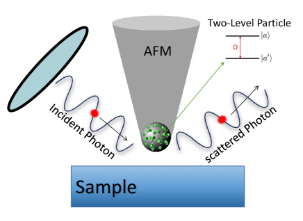
We investigate the interaction of near-field photons incident to an AFM tip, close to the surface of a dielectric sample. The goal is to study the effect of the dielectric material on the scattered photons from the AFM tip. As shown in Fig. 1, we consider an AFM tip, possessing atomic-size quantum dots (QDs), such as phosphorous (P) atoms doped in silicon (Si) [12, 13], Si-based dangling-bonds (DB) [14, 15, 16], or diamond-based nitrogen-vacancy (NV-) centers [17]. Incident photons interact with the tip and excite the quantum dots; as the QDs return to their ground state, photons are generated and scattered out of the tip. Since the AFM tip is placed close to the dielectric half-plane surface, spontaneous emission of photons from the AFM tip is modified at the presence of the dielectric surface, resulting in changes in the Fock state of the re-emitted photons.
To model the interaction between the AFM tip and the sample, we consider using the image theory. The AFM tip exposed by incident photons is modeled by an electric dipole. The sample is replaced by an effective image dipole containing the dielectric properties of the material, including the permittivity. The AFM tip is so close to the surface ( nm, the rim zone) that the near-field electrodynamics applies in this scale, and the van der Waals force is induced between the tip’s dipole and its image dipole in the sample. The effect of the sample on the scattered photons from the AFM tip, is modeled by employing modified second-order perturbation theory. Fock state of the scattered photons, which is carrying information about the properties of the dielectric material, is then calculated. Electrical properties of the material can be extracted from a quantum-spectroscopy setup [18, 19].
In the following sections, first we present the required information for modeling the proposed system. Then, quantum states of the desired system are obtained and the state of scattered photons from the AFM tip and the energy shift due to the presence of the sample are calculated. At the end, the concluding remarks are presented.
II Method
In this section, we elaborate on our proposed system. The system is composed of an AFM tip, exposed to incident photons, that is in close proximity to a dielectric sample. The AFM tip is close enough to the sample that the van der Waals interaction dominates. In the following, detailed description for the components of the proposed model is presented.
II.1 AFM Tip and the Induced Image Dipole
As illustrated in Fig. 2, an AFM tip exposed to incident photons can be modeled by a quantum electric dipole with the associated states given by and , and corresponding energies and , respectively. The energy difference between the two states, i.e. is proportional to the frequency of the incident photons.
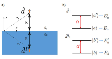
Assuming that the tip’s dipole is at a distance from the surface of the nearby dielectric sample, it results in an image dipole within the sample that is located at the same distance below the surface. According to the image theory, the whole effect of the half-space sample on the tip’s dipole can be modeled by considering its corresponding image dipole. As shown in Fig. 3, it is assumed that the charges of the image dipole are separated by the same distance as the main dipole, but with different charge values [20, 21]. The image of a single charge in a dielectric material is given by
| (1) |
where is the dielectric-air coefficient, which is a function of , i.e. the electric permittivity of the dielectric material.
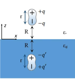
Many research groups have studied the coulomb energy of particle-surface interactions [22, 23]. Subsequently, the energies associated with the states of the image dipole (i.e. and ) are given by,
| (2) |
where and are the energies associated with the states of the AFM tip’s dipole. The same modification applies for the energy difference of the image dipole, i.e. .
Due to van der Waals interaction between the tip’s dipole and the image dipole, we expect to see a shift in the energy states of the tip’s dipole, caused by the image dipole. The effect of this interaction will be presented in Sec. II.3. In the following section, the role of incident photons on the AFM tip is discussed.
II.2 Photons Incident to the AFM Tip
To model photons incident to the AFM tip, we consider the near-field interaction. Study of electromagnetic waves (EM) and their quantum counterparts, i.e. photons, in an area very close to a material lies in the near-field electrodynamics, which is a great field of interest [24, 25, 26, 27].
As photons are reflected from the AFM tip, there are a few of them with imaginary k-vectors, called the evanescent photons, that decay as they pass through the very small area between the AFM tip and the nearby dielectric sample. As a consequence, spontaneous emission of the photons scattered from the AFM tip is modified due to the nearby dielectric sample. In other words, the presence of a dielectric material near to the AFM tip affects the incident photon and the tip interaction, resulting in a signature of the electric permittivity of the dielectric surface, in the quantum state of the photons scattered from the AFM tip.
Due to the near-field electrodynamics, interaction between the electric dipole of the tip and its image dipole is studied by the van der Waals force. This approach has many interest in scanning near-field optical microscopy [9]. To guarantee for being in the near-field region, hence ensuring the van der Waals interaction between the two dipoles, the distance between the AFM dipole and the corresponding image dipole should be small enough to satisfy,
| (3) |
where and are the Bohr frequencies of the dipoles [28], and are the position vectors of the dipoles, and is the speed of light in vacuum, see Fig. 2.
II.3 Van der Waals Interaction Between the AFM Tip and the sample
To model the tip-sample van der Waals interaction, we propose a modified perturbed Hamiltonian representing the AFM tip’s dipole and the image dipole interaction [29]. The effective perturbation Hamiltonian corresponding to the instantaneous dipole–dipole interaction is obtained by [28],
| (4) |
where and are the electric-dipole moment operators of the main dipole and the image dipole, respectively [28]. The parameter is the transverse delta function, representing the direction along the line passing through the dipoles. If the dipoles are polarized in the direction, as shown in Fig. 2, the inner product between the operators vanishes. The electric dipole operators are,
| (5) |
where is given by Eq. 1 and contains information about the permittivity of the sample, for is the electric dipole moment, and are the ladder operators defined by and . Eventually, the perturbed Hamiltonian turns to
| (6) | |||||
In the next section the effect of this perturbation on the quantum states of the photons, scattered from the AFM tip, is discussed.
III Quantum states and Energies of the System after Perturbation
Quantum states of the proposed system are comprised of the quantum states of the tip’s dipole, its image dipole in the dielectric sample, and the Fock state, , representing the photons incident on the AFM tip. These quantum states are given, in general, by
| (7) |
In the following, we study the effect of perturbation on these states.
III.1 Perturbed States
Since perturbation in the system results from the effect of the image dipole on the tip’s dipole, as presented in Eq. 4, there is no direct effect on the Fock state of the incident photons in the perturbation Hamiltonian. Furthermore, the first-order perturbation applies for charged particles, which is not the case for the dielectric sample, in our desired system. Therefore, modified second-order perturbation theory is implemented, and the resultant calculated perturbed states are given by,
| (8) |
where is the coefficient of the perturbed state . Similar results can be obtained for other three states.
Presuming to have a condition under which single photons interact with the AFM tip (for instance, having a single-photon emitter as a source of generating the incident photons), the state of such photons would be represented by . Then, the density matrix of our desired system would be a matrix given by,
| (9) |
where parameters for are the coefficients of every possible state in our system and are given by,
| (10) |
Suppose that using a proper mechanism, single photons scattered from the AFM tip, are detected by a single photon detector. These photons contain information about the electric properties of the dielectric sample. State of the scattered photons is obtained by reducing the state of the whole system, by tracing out the states of the subsystems associated with the AFM dipole and its image dipole interaction. Consequently, the state associated with the scattered photon is
| (11) |
Assuming that both dipoles are initially in their ground states, then only remains nonzero. Substituting its value from Eq. 10, the state of the scattered photon is obtained to be,
| (12) |
where is the coefficient of the unperturbed state . Equation 12 clearly shows that the state of a single scattered photon is bearing information about the properties of the dielectric sample, which is concealed in . Furthermore, the above equation demonstrates that the scattered-photon state depends on the distance of the tip from the sample, and the energy difference between the two states of the tip’s dipole, .
III.2 Energy Shift due to Perturbation
The effective perturbed Hamiltonian given by Eq. 4, leads to an energy change, , between the quantum states associated with the AFM tip, which is obtained by
| (13) |
This energy change is negative, indicating that the van der Waals interaction reduces the energy difference between the two states of the tip’s dipole, i.e. . Also, the amount of varies with , which is denoting that the tip-sample force is inversely proportional to . Consequently, the frequency of the photons scattered from the AFM tip is obtained by
| (14) |
The photons’ frequency contains information about the electrical properties of the dielectric material, which can be extracted from a quantum-spectroscopy setup [18, 19].
IV Conclusion
To conclude, we showed that the quantum behavior of an AFM tip exposed to incident photons is modified by existence of a dielectric material nearby. This modification is resulted by the van der Waals interaction between the tip’s dipole and an its image dipole, representing the properties of the dielectric. Finally, the Fock state of a scattered single photon is obtained through the perturbation theory and can be used to specify the permittivity of the dielectric material.
The discussed scheme with classical EM field incident to the AFM tip, is the key component for scattering scanning near-field optical microscopy (s-SNOM), which is a promising technique for overcoming Abbe diffraction limit. We speculate that replacing the classical incident EM field in this scheme, by a stream of photons, substantially helps in enhancing the spatial resolution. Therefore, the proposed quantum s-SNOM provides the opportunity for quantum imaging, quantum spectroscopy, and quantum sensing with higher spatial resolution.
References
- Pohl [1991] D. Pohl, Scanning near-field optical microscopy (snom) (Elsevier, 1991) pp. 243–312.
- Dürig et al. [1986] U. Dürig, D. W. Pohl, and F. Rohner, Near-field optical-scanning microscopy, Journal of applied physics 59, 3318 (1986).
- Harootunian et al. [1986] A. Harootunian, E. Betzig, M. Isaacson, and A. Lewis, Super-resolution fluorescence near-field scanning optical microscopy, Applied Physics Letters 49, 674 (1986).
- Betzig et al. [1987a] E. Betzig, M. Isaacson, and A. Lewis, Collection mode near-field scanning optical microscopy, Applied physics letters 51, 2088 (1987a).
- Betzig et al. [1991] E. Betzig, J. K. Trautman, T. Harris, J. Weiner, and R. Kostelak, Breaking the diffraction barrier: optical microscopy on a nanometric scale, Science 251, 1468 (1991).
- Betzig et al. [1987b] E. Betzig, M. Isaacson, and A. Lewis, Collection mode near-field scanning optical microscopy, Applied physics letters 51, 2088 (1987b).
- Zenhausern et al. [1995] F. Zenhausern, Y. Martin, and H. Wickramasinghe, Scanning interferometric apertureless microscopy: optical imaging at 10 angstrom resolution, Science 269, 1083 (1995).
- Porto et al. [2000] J. Porto, R. Carminati, and J.-J. Greffet, Theory of electromagnetic field imaging and spectroscopy in scanning near-field optical microscopy, Journal of Applied Physics 88, 4845 (2000).
- Knoll and Keilmann [2000] B. Knoll and F. Keilmann, Enhanced dielectric contrast in scattering-type scanning near-field optical microscopy, Optics communications 182, 321 (2000).
- Cvitkovic et al. [2007] A. Cvitkovic, N. Ocelic, and R. Hillenbrand, Analytical model for quantitative prediction of material contrasts in scattering-type near-field optical microscopy, Optics express 15, 8550 (2007).
- Majorel et al. [2020] C. Majorel, C. Girard, A. Cuche, A. Arbouet, and P. R. Wiecha, Quantum theory of near-field optical imaging with rare-earth atomic clusters, JOSA B 37, 1474 (2020).
- Chan et al. [2008] T.-L. Chan, M. L. Tiago, E. Kaxiras, and J. R. Chelikowsky, Size limits on doping phosphorus into silicon nanocrystals, Nano letters 8, 596 (2008).
- Melnikov and Chelikowsky [2004] D. V. Melnikov and J. R. Chelikowsky, Quantum confinement in phosphorus-doped silicon nanocrystals, Physical review letters 92, 046802 (2004).
- Livadaru et al. [2010] L. Livadaru, P. Xue, Z. Shaterzadeh-Yazdi, G. A. DiLabio, J. Mutus, J. L. Pitters, B. C. Sanders, and R. A. Wolkow, Dangling-bond charge qubit on a silicon surface, New Journal of Physics 12, 083018 (2010).
- Shaterzadeh-Yazdi et al. [2014] Z. Shaterzadeh-Yazdi, L. Livadaru, M. Taucer, J. Mutus, J. Pitters, R. A. Wolkow, and B. C. Sanders, Characterizing the rate and coherence of single-electron tunneling between two dangling bonds on the surface of silicon, Physical Review B 89, 035315 (2014).
- Shaterzadeh-Yazdi et al. [2018] Z. Shaterzadeh-Yazdi, B. C. Sanders, and G. A. DiLabio, Ab initio characterization of coupling strength for all types of dangling-bond pairs on the hydrogen-terminated si (100)-2 1 surface, The Journal of Chemical Physics 148, 154701 (2018).
- Schirhagl et al. [2014] R. Schirhagl, K. Chang, M. Loretz, and C. L. Degen, Nitrogen-vacancy centers in diamond: nanoscale sensors for physics and biology, Annu. Rev. Phys. Chem 65, 83 (2014).
- Mukai et al. [2021] Y. Mukai, M. Arahata, T. Tashima, R. Okamoto, and S. Takeuchi, Quantum fourier-transform infrared spectroscopy for complex transmittance measurements, Physical Review Applied 15, 034019 (2021).
- Lindner et al. [2020] C. Lindner, S. Wolf, J. Kiessling, and F. Kühnemann, Fourier transform infrared spectroscopy with visible light, Optics express 28, 4426 (2020).
- Jackson [1999] J. D. Jackson, Classical electrodynamics (1999).
- Hammond [1960] P. Hammond, Electric and magnetic images, Proc. IEE 107, 306 (1960).
- Mavroyannis [1963] C. Mavroyannis, The interaction of neutral molecules with dielectric surfaces, Molecular Physics 6, 593 (1963).
- Zaremba and Kohn [1976] E. Zaremba and W. Kohn, Van der waals interaction between an atom and a solid surface, Physical Review B 13, 2270 (1976).
- Pohl and Courjon [2012] D. W. Pohl and D. Courjon, Near field optics, Vol. 242 (Springer Science & Business Media, 2012).
- Girard and Dereux [1996] C. Girard and A. Dereux, Near-field optics theories, Reports on Progress in Physics 59, 657 (1996).
- Courtois et al. [1996] J.-Y. Courtois, J.-M. Courty, and J. Mertz, Internal dynamics of multilevel atoms near a vacuum-dielectric interface, Physical Review A 53, 1862 (1996).
- Feron et al. [1993] S. Feron, J. Reinhardt, S. Le Boiteux, O. Gorceix, J. Baudon, M. Ducloy, J. Robert, C. Miniatura, S. N. Chormaic, H. Haberland, et al., Reflection of metastable neon atoms by a surface plasmon wave, Optics communications 102, 83 (1993).
- Keller [2012] O. Keller, Quantum theory of near-field electrodynamics (Springer Science & Business Media, 2012).
- Feinberg and Sucher [1970] G. Feinberg and J. Sucher, General theory of the van der waals interaction: A model-independent approach, Physical Review A 2, 2395 (1970).
- Bell [2012] R. Bell, Introductory Fourier transform spectroscopy (Elsevier, 2012).
- Malherbe et al. [2012] O. Malherbe, P. J. Scott, and P. Selinger, Partially traced categories, Journal of Pure and Applied Algebra 216, 2563 (2012).