Doped Semiconductor Devices for sub-MeV Dark Matter Detection
Abstract
Dopant atoms in semiconductors can be ionized with meV energy depositions, allowing for the design of low-threshold detectors. We propose using doped semiconductor targets to search for sub-MeV dark matter scattering or sub-eV dark matter absorption on electrons. Currently unconstrained cross sections could be tested with a 1 g-day exposure in a doped detector with backgrounds at the level of existing pure semiconductor detectors, but improvements would be needed to probe the freeze-in target. We discuss the corresponding technological requirements and lay out a possible detector design.
I Introduction
A variety of strategies have been explored and proposed to directly detect dark matter (DM) via the interactions that it may have with the Standard Model (SM) particles. One possibility is to design detectors that look for excitations of a material as the DM scatters off or is absorbed in it. The sensitivity of such experiments at low DM masses is fundamentally limited by the minimum energy required to create an excitation in the material. Currently, several leading constraints on DM with masses below a GeV are set by detectors that look for DM-electron interactions using semiconductor targets, where thresholds are set by the ionization energy of the valence-band electrons (the bandgap), which is typically of order eV Essig:2011nj ; Tiffenberg:2017aac ; Crisler:2018gci ; Agnese:2018col ; Abramoff:2019dfb ; Aguilar-Arevalo:2019wdi ; SENSEI:2020dpa ; Arnaud:2020svb ; Amaral:2020ryn ; DAMIC-M:2022aks . This is sensitive to DM scattering or absorption for DM masses exceeding MeV or eV, respectively.
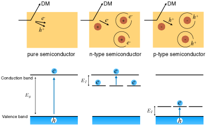
We propose to extend the reach of semiconductor detectors towards lower DM masses through a simple innovation: adding shallow impurities to the semiconductor. Shallow impurities, also called dopants, are atoms that introduce new energy levels close to the conduction band (n-type dopant) or valence band (p-type dopant), which are populated by electrons or holes contributed by the n- or p-type atoms. By emitting these charges into the conduction or valence bands, dopants can be ionized with sub-bandgap energy depositions, as schematically shown in Fig. 1. Since the dopant’s electrons or holes are weakly bound, their orbits lie far from the impurity centers, so the ionization energies are largely independent of the details of the dopant and are instead mostly set by the macroscopic properties of the underlying semiconductor PhysRev.97.869 ; PhysRev.98.915 ; kohn1957shallow ; shklovskii2013electronic . In this simplified picture the smallness of the energy required to ionize a dopant can be quantified by accounting for the screening of the impurity potential due to the semiconductor’s dielectric function , and for the smallness of the effective electron or hole masses compared to the electron mass in vacuum, typically . These two factors suppress the ionization energy by roughly with respect to the one of a free atom, resulting in energies of order meV. Such low thresholds allow designing ionization detectors that can be used to probe sub-MeV DM scattering or sub-eV DM absorption. In doped semiconductors, DM can also ionize valence-band electrons, so a doped target retains the signatures of pure semiconductor targets for eV energy depositions.
For models of DM scattering off electrons via a light mediator, we find that a doped target with an exposure of 100 g-day could probe the entire currently unconstrained sub-MeV mass region for DM produced via freeze-in Essig:2011nj ; Chu:2011be ; Dvorkin:2019zdi , in the absence of dark counts (DC). For sub-eV dark-photon DM absorbed by electrons, an exposure as small as 1 gram-day with DC at the level of existing undoped detectors could probe currently unconstrained absorption cross sections.
Our proposal has the advantage that it could largely rely on existing technology. Doped semiconductor detectors have been fabricated for decades for infrared (IR) light detection rogalski2002infrared ; rogalski2019infrared . Due to the nature of their applications (e.g., infrared astronomy) the DC requirements on existing detectors are above what is needed for DM detection rieke2007infrared . However, single-electron sensitivity with small DC has been demonstrated in pure semiconductor detectors that collect charge such as SENSEI ( DC/g-day) SENSEI:2020dpa ; SENSEI:2021hcn or phonons, such as SuperCDMS HVeV SuperCDMS:2020ymb , and they could be further reduced with detector improvements SENSEI:2020dpa . Thus, our proposal could be realized by combining the design of existing doped semiconductor detectors with the technologies used to obtain low DC in undoped detectors.
While in the body of this work we focus on studying ionization signals, for energy depositions below the dopant’s ionization threshold, doped targets allow for transitions between the ground and excited electron or hole bound states. Upon relaxation to the ground state, phonons are emitted, which could be potentially detected with future single-phonon detectors. We leave the discussion of phonon signals to an appendix.
We organize this work as follows. We begin by reviewing the theory of electrons in doped semiconductors, focusing on n-type dopants (the situation for p-type dopants is analogous). We then compute the energy loss function due to ionization in these materials, obtain DM scattering and absorption rates, and project the detector’s reach for a silicon target doped with phosphorus. In the Supplemental Materials, we discuss detector design, backgrounds, other low-threshold detection technologies, the expected phonon signals, and calculational details.
II Electronics of N-type Doped Semiconductors
The electronic wavefunctions in a perfect crystal potential are given by Bloch wavefunctions , where labels the crystal momenta, is a band index, and are functions with the periodicity of the lattice. For donor electrons in n-type semiconductors the spectrum differs from the perfect lattice solution due to the impurities. In this case, the wavefunctions can be expressed as a Bloch-state superposition PhysRev.97.869 ; PhysRev.98.915 ; kohn1957shallow ; shklovskii2013electronic ,
| (1) |
where is the semiconductor’s volume, and the Fourier coefficients are found by solving Schrödinger’s equation for in the impurity and lattice potentials. The impurity potential can be approximated by the one of a ionic charge screened by the lattice,
| (2) |
where is the fine-structure constant, and is the crystal’s dielectric function. The crystal potential is more complex and leads to dependency of the wavefunctions on the band structure. Full knowledge of the bands, however, is not required to obtain approximate wavefunctions, as donor electrons bind only weakly to the impurity so their typical momentum lies close to the bottom of the conduction band. This leads to two simplifications. First, the wavefunctions in Eq. (1) can be approximated to be those at the (possibly degenerate) conduction band minima. Fixing the band index to correspond to the conduction band and dropping it, and taking the momentum coordinate of the -th degenerate conduction-band minimum to be , this corresponds to approximating , so the wavefunction Eq. (1) for an electron with momentum close to the -th minimum simplifies to
| (3) |
where and is now the momentum relative to the band minimum. Eq. (3) indicates that donor electrons are described by bottom-of-band Bloch wavefunctions modulated by an “envelope” , which is the same for all degenerate minima .
The second simplification is that near the band minima, band energies can be approximated by the leading term in a momentum expansion,
| (4) |
where we have assumed isotropy in momentum space for simplicity (“spherical” band approximation), and is the electron’s effective mass.111The spherical-band approximation is not precise in indirect bandgap semiconductors such as Si and Ge where the bands are anisotropic. However, as discussed in the appendix, treating the bands as spherical will suffice for our purposes. With these approximations, the envelope functions and energy eigenvalues can be shown to be solutions of the Schrödinger equation with a Hamiltonian set by the screened impurity potential Eq. (2) and the kinetic term Eq. (4) PhysRev.97.869 ; PhysRev.98.915 ; kohn1957shallow ; shklovskii2013electronic ,
| (5) |
The solutions to Eq. (5) are Hydrogenic, so the energies (relative to the conduction band), Bohr radius of the bound electrons, and ground-state envelope function are
| (6) |
where is the principal quantum number. For typical values of and , the ionization energies are of order meV. The Bohr radius of a dopant electron is times larger than typical lattice spacings , so its typical momentum lies near the origin of the first Brillouin zone, , validating the bottom-of-band approximation. With our approximations both the ionization energy and Bohr radius are independent of the dopant atom, as anticipated in the introduction.
The model described above is the simplest version of the “effective-mass method” PhysRev.97.869 ; PhysRev.98.915 . Corrections to the model arise from wavefunction overlap of electrons localized at different impurities, electron-electron interactions, and differences in the impurity potential at different sites. These corrections lead to dispersion in the discrete energies Eq. (6) and thus to “impurity bands”. For high doping ( for uncompensated Si:P swartz1960low ; yamanouchi1967electric ; lohneysen1990metal ), these bands allow for electric conduction as in a metal, resulting in a metal-insulator Mott-Anderson transition mott1949basis ; anderson1958absence and eliminating the energy gap that is required for the design of ionization detectors. Here we only consider semiconductors with doping densities below the Mott value. Additional corrections to the effective-mass method come from short-distance modifications to the impurity potential Eq. (2) that break the degeneracy of the band minima aggarwal1965optical ; shklovskii2013electronic . For Si, these corrections lead to a ground-state that is set by a superposition of the Bloch wavefunctions at the degenerate minima, modulated by the common 1s envelope of Eq. (6) (see appendix).
While up to now we have only considered donor electron bound states, the presence of impurities also affects the conduction-band electron wavefunctions, which are relevant as final states for computing ionization probabilities. The modified conduction-band electron wavefunctions are simply given by Eq. (3), with envelope functions set by the positive-energy solutions of the Schrödinger Eq. (5); they are given by holt1969matrix
where and are the Gamma and confluent hypergeometric functions.
III Dark matter detection using doped semiconductors
In a doped semiconductor, DM can interact with both valence band and dopant electrons. Since the typical momentum and energy transfer relevant for ionizing dopant electrons are well separated from those for ionizing valence-band electrons, we can treat these two processes independently. The interaction rate on valence-band electrons happens as in pure semiconductors and has been computed in Essig:2011nj ; Graham:2012su ; Lee:2015qva ; Essig:2015cda ; Derenzo:2016fse ; Griffin:2019mvc ; Trickle:2019nya ; Griffin:2021znd ; Hochberg:2021pkt ; Knapen:2021run ; Knapen:2021bwg ; Trickle:2022fwt ; An:2014twa ; Bloch:2016sjj ; Hochberg:2016sqx . Here we focus instead on obtaining the single-ionization rate of DM interactions with the dopant electrons. Secondary ionization of other dopants by the excited electron are unlikely given the large separation between dopants for doping densities below the Mott transition, so they are not computed here.
We consider two example DM models. First we take a DM particle scattering with electrons via ultralight vector mediator (“dark photon”) that kinetically mixes with the SM photon with mixing parameter Holdom:1985ag ; Galison:1983pa , so that the momentum-space low energy potential coupling with electrons is
| (7) |
where is the coupling between and the mediator, the elementary charge, and the mediator mass has been neglected with respect to the momentum transfer. Second, we consider a model where the kinetically-mixed vector field itself is the DM, which can be detected by absorption on electrons.
Dark matter scattering: the DM scattering rate per unit target mass is Hochberg:2021pkt ; Kahn:2021ttr
| (8) |
where , and are the DM and target mass densities (for Si ), is the DM velocity distribution in the halo Drukier:1986tm , with dispersion, escape, and earth velocities , , and (in the galactic frame). is the scattering rate of a single DM particle with velocity in the whole target, given by
| (9) |
with being the energy transfer, is given by Eq. (7), and the energy loss function (ELF) is
| (10) |
where the number density of dopants and is the momentum-space electron-density operator. In Eq. (10), we have already performed the sum over target electrons, so there is a factor of from multi-particle screening Trickle:2019nya ; Hochberg:2015fth ; Kahn:2021ttr , and the term in brackets is the single-particle form factor between the initial (ground) state and free conduction-band electrons with momentum close to the -th minimum. This form factor is obtained in the appendix, where we show that within the effective mass method described previously, and for momentum transfers less than the inverse lattice spacing, , it is given by the form factor between the initial (bound) and free Hydrogenic envelope functions and
| (11) |
For ionization from the 1s ground state Eq. (6) into the free states Eq. (II), Eq. (11) has been analytically computed in holt1969matrix ; Chen:2015pha . Using the result of holt1969matrix in Eq. (10) we obtain the ELF for n-type doped semiconductors
where and is the momentum of the final state electron for an energy transfer . In Eq. (III), we have heuristically added a normalization prefactor to account for the ratio of local electric field at the donor center and the average field in the crystal, as done in photoionization calculations dexter1958theory ; anderson1975shallow ; sclar1984properties .
Dark matter absorption: the rate per unit mass for the absorption of kinetically-mixed vector DM is simply Mitridate:2021ctr , where the ELF is given by Eq. (III).
IV Projected reach
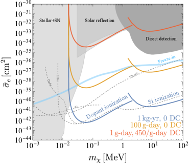
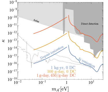
We now compute the projected DM reach taking for concreteness silicon doped with phosphorus as the target. For this material, the parameters entering in the ELF Eq. (III) are set to meV, , atomic units, and , as discussed in the appendix. The resulting projections for DM scattering and absorption are presented in Fig. 2, where in both cases the phosphorus density is . This density is chosen to maximize the number of target electrons while staying below the metal-insulator transition. For DM scattering, the bounds are presented as a function of the reference cross section on electrons , where is the DM-electron reduced mass. For DM absorption the bounds are presented as a function of the photon-dark photon mixing parameter . Bounds are presented for three assumptions regarding dark counts (DC) and exposure. In blue and green we present limits for kg-year and 100 g-day exposures that consider only Poisson statistical uncertainties and assume no DC are observed. In red we project more conservative sensitivities with exposures and DC in line with SENSEI at MINOS SENSEI:2020dpa , that is a 1 g-day exposure and 450/g-day DC. Each projected exclusion curve is broken into two pieces to highlight the reach due to the ionization of dopants (masses below MeV or eV for scattering or absorption), or due to the ionization of valence band electrons (for larger masses).222The Si ionization sensitivity projections include screening, and hence the 1 g-day curve assuming a DC of 450/g-day is weaker than the SENSEI limit shown in gray SENSEI:2020dpa .
Our projections show that doped semiconductor targets have a significant discovery potential, and compare favorably against other proposed targets. From the figures we clearly see how introducing doping into the material extends the reach of semiconductor detectors to lower DM masses. In Fig. 2, we see that in the absence of DC, doped semiconductors have the potential to probe scattering cross sections that lead to DM being produced by freeze-in down to the smallest allowed masses, keV. The excellent reach to DM scattering is in part explained by kinematic matching, as for the typical momentum tranfers , with () being the dopant electron velocity, the energy transfers are precisely of the order of dopant ionization energies, meV. The kinematics are further studied in the appendix, where we present differential scattering rates. The right panel of Fig. 2 indicates that Si:P also has excellent reach to dark-photon absorption for DM masses eV. For DM absorption, even with a small 1 g-day exposure and if DC are included in our estimates at the level currently observed by SENSEI, our proposal could probe currently unconstrained parameter space.
V Discussion
We have proposed a new DM detection strategy based on looking for DM interactions on dopant atoms. By computing DM interaction rates, we have shown that doped semiconductor targets have the potential to explore large regions of parameter space of two benchmark DM models, sub-MeV DM coupling to the SM via a light mediator, and kinetically-mixed sub-eV dark-photon DM. This work begins the exploration of doped sub-MeV DM detectors. From the theoretical side, interaction rates on other doped targets and calculations of the Migdal effect on dopants will be required, while from an experimental perspective developments for the detector design are needed, as discussed in the appendix. We conclude that the development of doped semiconductor detectors with low dark counts is both scientifically and technologically motivated, and may lead to the discovery of DM.
VI Acknowledgments
We would like to thank Steve Holland, Junwu Huang, Noah Kurinsky, Guillermo Moroni, Sae Woo Nam, Roger Romani, Miguel Sofo Haro, Javier Tiffenberg, and Sho Uemura for useful discussions. The work of P.D. is supported by the US Department of Energy under grant DE-SC0010008. D.E.U. is supported by Perimeter Institute for Theoretical Physics and by the Simons Foundation. Research at Perimeter Institute is supported in part by the Government of Canada through the Department of Innovation, Science and Economic Development Canada and by the Province of Ontario through the Ministry of Economic Development, Job Creation and Trade. R.E. acknowledges support from DoE Grant DE-SC0009854, Simons Investigator in Physics Award 623940, the US-Israel Binational Science Foundation Grant No. 2016153, and the Heising-Simons Foundation Grant No. 79921. M.S. acknowledges support from Department of Energy Grants DE-SC0009919 and DE-SC0022104.
VII Supplementary Material
VII.1 Detector design and backgrounds
To realize the discovery potential of doped semiconductor targets a scalable single-electron detection technology with low dark counts is required. Here we discuss one possible implementation, based on the Skipper-CCD detectors used by the SENSEI experiment SENSEI:2020dpa . Skipper-CCDs are imaging detectors that use high-resistivity n-type Si as the bulk absorber to detect ionization signals. Even if the target is n-type, these CCDs are not doped ionization detectors, since their doping density is extremely small, on the order of , and since they are operated at temperatures where the dopants are already ionized. Skipper-CCDs have demonstrated single electron-hole-pair resolution and dark counts as low as events per gram-day SENSEI:2020dpa . Building upon this technology, we envision designing a Skipper-CCD with a large level of n-type doping in the bulk.333A detector that instead measures ionization signals by reading out phonons such as SuperCDMS HVeV could also be considered, but the current single-electron dark current in such detectors is larger than at SENSEI by a factor of SuperCDMS:2020ymb . In addition, SuperCDMS HVeV, at least in its current setup, would reject a single-electron or single-hole signal from an ionized dopant, as its single-electron bin corresponds only to events that are electron-hole pairs.
The design of a doped Skipper-CCD would require several technological developments. For concreteness, we discuss these developments in the context of n-type targets (the situation for p-type detectors is analogous). First and foremost, current n-type Skipper-CCDs used for detecting DM only collect holes, and they do so in a “buried channel” located right below the detector’s frontside where charges are stored until readout. For our proposal to be realized, a doped n-type Skipper-CCD needs to collect ionized electrons from n-type dopants. A detailed design that satisfies this requirement will be presented in future work.
In order to collect the charge signals, and to ensure low levels of charge trapping, the detector would need to be placed in an electric field (as a conventional CCD), which would be provided by a bias voltage applied to detector contacts. Since the active area would be doped, this electric field would also induce currents within the “impurity band” formed by the dopant’s energy levels, without the need for electrons being excited into the conduction band (“hopping conductivity” PhysRev.79.726 ), which would constitute a dark current. A technology to eliminate this current exists, which is used in a type of doped semiconductor detectors called “Blocked Impurity Band” detectors petroff1986blocked (BIBs). The idea is to introduce a layer of undoped semiconductor between the active detection region and the charge readout stages, which in our case are the buried channels, so that impurity band conduction is blocked. BIBs that operate with high levels of doping have quantum efficiencies of the order of for V of applied voltage across an absorber that is tens of m wide rogalski2019infrared , which also indicates that charge trapping in these devices is under control. This also suggests that charge transfer across pixels (which is required for readout in a CCD-like setup) could be done efficiently even if the target is doped.
In order to suppress thermal generation of dark currents due to the ionization of dopants, the detector would need to be operated at cryogenic temperatures. The rate for the thermal generation of electrons from neutral donors can be estimated to be from detailed balance MARTINI1972181 . Here is the effective density of states of electrons in the conduction band, is the cross section for electrons capture by charged donors, and indicates the thermal average. From measurements, we obtain for Si:P PhysRev.144.781 . Therefore, thermal dark currents would be kept at the level of for by operating the detector at a temperature K (meV).
The low operating temperatures represent a challenge for a doped detector based on a CCD design, since conventional CCDs cannot operate at temperatures below K due to carrier freeze-out janesick1987scientific , where the gates become non-conducting. This issue could be solved by replacing the standard polysilicon gates with metal gates, as done in some metal oxide semiconductor (MOS) devices.
In addition to thermally generated dark counts, it is likely that a doped Skipper-CCD would be affected by the backgrounds that are observed in undoped Skipper-CCDs. The origin of the currently observed backgrounds in Skipper-CCDs is unknown, even if a fraction of them have been shown to arise from secondary radiation of high energy tracks Du:2020ldo ; SENSEI-radiative-to-appear . Track-induced “extrinsic” backgrounds can be reduced by working in a radio-pure environment and improving shielding. The “intrinsic” detector backgrounds in Skipper-CCDs, on the other hand, could arise from charge leakage into the detector contacts, or from slow release of electrons from unidentified traps. Both of these effects could in principle be reduced by improving the insulating layers and pre-filling empty traps. On the other hand, the intrinsic dark counts that are observed in doped blocked-impurity band detectors are possibly coming from conduction across the blocking layers into the contacts wang2016analysis ; marozas2018surface ; pan2021dark , either via tunneling or due to impurities. Such dark currents could be suppressed by increasing the thickness of the insulating layers wang2016analysis . Yet another source of dark counts in doped detectors arises due to conduction within the impurity band by hopping into neutral (occupied) dopants, a process that’s referred to as hopping conductivity 1971JETPL..14..185G ; shklovskii2013electronic . This can be exponentially suppressed by reducing the doping density, but measurements are required to find an optimal doping value.
We conclude this section by pointing out that several other detector targets with sub-eV thresholds exist, beyond doped semiconductors, which are used to detect infrared (IR) radiation but that can also be used to detect sub-MeV DM scattering or sub-eV dark photon absorption. We provide an incomplete list of available IR detectors in Table 1, which includes Superconducting nanowire detectors (SNPDs), Single-photon avalanche diodes (SPADs), Mercury-Cadmium-Telluride detectors (HgCdTe), the already mentioned BIBs, Quantum Dot and Quantum Well Infrared Photodetectors (QDIP and QWIP) and Transition Edge Sensors (TES). These detectors can be designed and used as targets for DM absorption or scattering, or in some cases can be coupled to read out excitations from an external absorber that acts as the target.
SNSPDs were proposed as sub-MeV dark-matter targets in Hochberg:2019cyy , but an order-of magnitude increase in detector exposure (without a corresponding increase in dark currents) would be needed to probe regions of parameter space that are not currently excluded by astrophysical searches Hochberg:2021yud . Current nanogram-scale SNSPD detectors have dark counts of the order of Hz. The origin of dark counts in SNSPDs is currently unknown, but it is possible that they arise from secondary emission from environmental high-energy radiation Du:2020ldo , or due to micro-fractures upon detector cooling Anthony-Petersen:2022ujw . Both of these dark count sources increase with detector exposures. SNSPDs have also been used as detectors to measure interaction events of DM on an external dielectric stack target Baryakhtar:2018doz ; Chiles:2021gxk , and have also been proposed as photodetectors, to detect the photons that arise from DM with masses 1 MeV interacting in a nearby scintillating target Derenzo:2016fse ; Essig:2019kfe ; Blanco:2019lrf ; Blanco:2022cel .
Another possibility is to consider detectors based on low-bandgap compounds of the III-V groups. One of the most mature single-photon detection technologies where these compounds have been used are single-photon avalanche diodes, or SPADs. These detectors have the advantage that they be operated at significantly higher temperatures than SNSPDs, but suffer from larger dark currents dello2022advances , likely due to tunneling huang2020high . A type of SPADs (“Silicon Photomultipliers” or SIPMs) have been proposed to study DM scattering with an energy threshold of eV SIPM , but to our knowledge the potential of SPADs as sub-MeV DM detectors has not been explored.
| Detector type | Energy gap (eV) |
|---|---|
| SNSPD Chiles:2021gxk | |
| III-V SPAD zhang2015advances | |
| Hg1-xCdxTe doi:10.1146/annurev.astro.44.051905.092436 | 0.5 () |
| 0.1 () | |
| Doped semiconductor | (Si:P, Si:As) |
| BIB doi:10.1146/annurev.astro.44.051905.092436 | (Ge:Ga) |
| (GaAs:Te) | |
| QDIP Campbell20071815 | (InAs/InGaAs) |
| QWIP ROGALSKI1997295 | (GaAs/AlGaAs) |
| TES ROGALSKI1997295 |
Yet another option is to consider detectors based on Mercury-Cadmium-Telluride (HgCdTe), a compound that has the advantage that its bandgap can be tuned, in principle down to the metallic transition rogalski2019infrared . HgCdTe detectors are widely used in astronomy for near and mid-infrared detection, but to the best of our knowledge no HgCdTe-based detector has demonstrated single-photon detection, which would be a requirement for searching for sub-MeV DM scattering or sub-eV DM absorption. Significant progress, however, is being made to achieve IR single-photon detection using photodiodes based in HgCdTe dello2022advances .
Going towards the deep infrared, doped semiconductor BIBs offer some of the leading sensitivities. That being said and as already discussed in the body of this work, existing BIBs suffer from dark counts that are too large for the purposes of detecting DM.
Other more recently developed technologies are quantum well and quantum dot detectors. Regarding these detectors, here we only point out that quantum dots have been proposed as targets for DM scattering Blanco:2022cel , but to our knowledge their potential as photodetectors detectors to search for photons from DM interactions in a nearby target has not been explored.
Finally, TES have been proposed as sub-MeV DM detectors in a setup where DM interacts with an external absorber creating phonons, which are then read out by TES located in the absorber’s surface Hochberg:2015fth ; Hochberg:2015pha ; Hochberg:2016ajh ; SPICE , but order-of-magnitude improvements in the TES’s energy thresholds are required to probe such light DM models ren2021design . Like SNSPDs, TES have also been proposed as a photodetector to detect photons from DM with masses 1 MeV interacting in a nearby scintillating target Derenzo:2016fse ; Essig:2019kfe ; Blanco:2019lrf ; Blanco:2022cel . Dark currents for TES’s are briefly discussed in the section “Sub-ionization energy depositions and phonon signals”.
VII.2 Phosphorus-doped Silicon ELF parameters
In this appendix, we discuss our choices for the numerical values of the parameters entering into the ELF Eq. (III) for the specific case of silicon doped with phosphorus, Si:P. First, we set the ionization energy to the experimentally measured value, meV aggarwal1965optical ; ning1971multivalley . For the Coulomb impurity potential and spherical band approximations used to obtain the ELF, Eq. (6) sets the relations that allow the effective mass and Bohr radius to be calculated from the ionization energy. These relations (and more generally the effective mass method used in this work) must be regarded only as a rough approximation for Si, as for this material the band structure around the minimum is anisotropic, the impurity potential deviates from the Coulomb form near the impurity ion, and intervalley couplings modify the spectrum aggarwal1965optical ; ning1971multivalley . In order to account for these corrections, we use the phenomenological prescription of ning1971multivalley , which has been demonstrated to correctly describe the experimentally measured energy levels in Si:P. The prescription retains the spherical band approximation and the Hydrogenic form of the envelope functions (so we may retain the form of the ELF Eq. (III)), but treats as a free parameter that is determined by matching the ground state energy levels obtained with the spheroidal and realistic ellipsoidal band case in Si, and as a variational parameter that is chosen to minimize the full Hamiltonian including short-distance and intervalley corrections. This results in and atomic units ning1971multivalley . For the screening prefactor in the denominator of Eq. (III), , we simply approximate , which leads to a small error of order in the calculations doi:10.1143/JPSJ.20.778 ; doi:10.1143/JPSJ.21.1852 . Finally, we set the normalization prefactor to to match the normalization of measurements of the dielectric function in Si:P at (i.e., photoabsorption measurements) reported in thomas1981optical ; gaymann1995temperature , by using the relation
| (13) |
evaluated at . In order to validate our calculation of the ELF, we have compared our results with the frequency-dependent photoabsorption data of thomas1981optical ; gaymann1995temperature and confirmed that it correctly reproduces the data (see section below on ELF validation). Note that by using Eq. (13), it is in principle possible to obtain the ELF directly from measurements of the material’s dielectric constant instead of using our computation, Eq. (III). To our knowledge, however, no measurements of in Si:P away from have been performed, and even at the dielectric function has only been measured over a limited range of frequencies, so in what follows we rely on Eq. (III) for obtaining DM interaction rates and calculating projections.
VII.3 Form factor derivation
In this section, we calculate the form factor for dopant electron transitions between the ground state and free conduction-band energy levels. We begin by defining Bloch wavefunctions for conduction-band electrons as
| (14) |
where the index specifies one of the possibly degenerate conduction-band minima and its position in momentum space, labels crystal momenta measured from this minimum, and is the semiconductor’s volume. The periodic functions are set to be unit-normalized in ,
| (15) |
and Bloch wave-functions are orthonormal,
| (16) |
As discussed in the section Electronics of Doped Semiconductors, the initial (ground) state and final single-particle states are given by a sum of conduction-band Bloch wavefunctions,
| (17) | |||||
| (18) |
where the coefficients setting the components of the wavefunctions at the different minima are normalized as
| (19) |
As an example, for the Si ground state, which is relevant for our limit projections, the initial ground state is a singlet s-wave state formed by equal-weight superpositions of the wavefunctions at these minima, modulated by the 1s envelope function of Eq. (6),
| (20) |
so for Si, .
Now, the form factor for transitions between the initial and final states is given by
where is the momentum-space electron density operator. Given that the different conduction band minima in typical semiconductors such as Si and Ge are separated by distances of order keV in momentum space, with being the lattice spacing, for momentum transfers keV the generator of momentum translations does not connect different conduction band minima, and we obtain the simplification
| (22) |
This simplification is valid for sub-eV absorption in the semiconductor, where eV, and for sub-MeV DM scattering via a light mediator, where we have checked that the typical momentum transfer is , with . Inserting Eq. (22) in Eq. (LABEL:eq:form1) we obtain
and using Parseval’s theorem on Eq. (LABEL:eq:form2), we get
where we defined Fourier transforms as that are unit-normalized in the target volume. Now, take the final state to be so . Then Eq. (LABEL:eq:form3) simplifies to
Finally, summing over the final-state minima and using the normalization condition Eq. (19) we obtain
which is the result quoted in Eq. (11).
VII.4 ELF validation and comparison
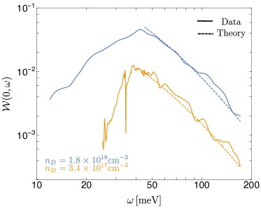
In this section, we validate our analytical approximation of the ELF in Si:P (Eq.(III)) by comparing it to experimental data and alternative analytic ELF computations. To our knowledge, only optical data is available for Si:P, meaning only is determined by experiments (within a range of measured frequencies). In Fig. 3, we show for Si:P calculated from the measurement of optical reflectance with two doping densities PhysRevB.52.16486 ; PhysRevLett.71.3681 , and we also present our analytical hydrogenic ELF Eq. (III). For both doping densities, the hydrogenic ELF matches the data very well for energies above the ionization threshold meV.
To check the robustness of the hydrogenic ELF at finite , we compare it with another analytical expression for the ELF proposed by Mermin, where an empirical formula of the dielectric function, or equivalently the ELF, is provided with coefficients to be fitted from data. The Mermin ELF relevant for dopants in Si has the following form:
| (27) |
where is the Mermin dielectric function defined as Mermin:1970zz
| (28) |
Here is Lindhard dielectric function derived from the free electron gas
| (29) |
with and
| (30) |
Taking the limit of Eq. (27), one gets
| (31) |
In Eq. (31), , , and are fitting parameters that are determined by matching to data. After fitting to optical data for Si:P with above the ionization energy meV, we get , meV, and meV.
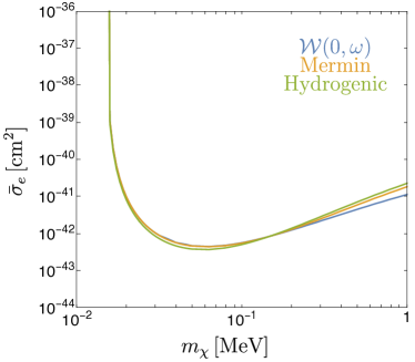
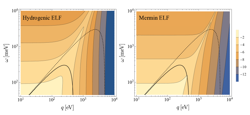
We then evaluate the impact of the different ELFs on our computations in Fig. 4, where we compare the DM rate for dopant ionization in the same material as above (Si:P with ), calculated from the Hydrogenic and Mermin ELFs. In the figure we have assumed that scattering occurs via a light dark photon mediator. Our results indicate that the rates obtained from the Hydrogenic and Mermin ELFs agree well with each other in the whole sub-MeV region of DM masses. The two approaches are further compared in Fig. 5, where we show contours of the ELFs as a function of momentum and frequency. From the figure we observe that at low momentum transfers compared with the characteristic momentum scale of the ELFs, , both ELFs are similar, and start to differ only at larger momentum transfers. This feature explains in part the broad agreement of the rates obtained using the two ELFs, as for sub-MeV DM scattering via a light mediator the typical momentum transfer is precisely , except for masses near an MeV. Nevertheless, the momentum-dependency of the ELF is relevant at large DM masses. This is shown in Fig. 4, where we also present in blue the rate obtained from purely from an interpolation of optical data. We see that this approach starts to differ from the momentum-dependent Hydrogenic and Mermin ELFs for near 1 MeV, which indicates that momentum-dependent terms in the ELFs become relevant for such masses.
VII.5 Differential rate of DM scattering on dopant electrons
In this section, we study the differential rate for DM ionizing dopant electrons. The general for DM scattering with electrons in a target is given as:
| (32) |
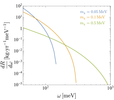
where , and . As mentioned in the main text, we use the hydrogenic ELF in Eq. (III) to describe single-electron ionization from DM scattering with dopants. In Fig. 6, we show the differential rate for DM scattering in a Si:P target with a light dark photon mediator for several DM masses. For all cases, the spectra are peaked at the ionization threshold meV and rapidly decrease for larger . This feature results from the combination of the kinematics of the light mediator scattering and the ELF. Therefore, the dominant contribution to the total rate comes from the low energy transfer. There is also a sharp cut-off of the spectrum at , which is the maximum energy transfer allowed for a given DM mass.
VII.6 Sub-ionization energy depositions and phonon signals
When the energy transfer to the dopant atom falls below the ionization threshold, dopant electrons are excited into higher-energy bound states that relax back to the ground state by emitting acoustic phonons, which can potentially be measured with calorimetry. To evaluate the DM discovery potential of these sub-ionizing signals, we compute here the contribution of bound-to-bound transitions to DM scattering and absorption rates.
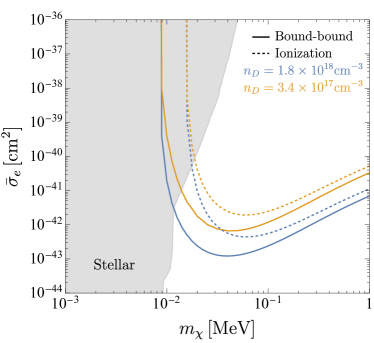
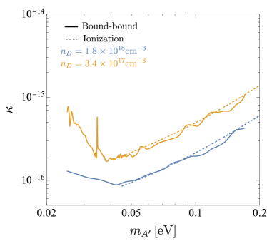
DM interaction rates below the ionization threshold are not captured by the Hydrogenic ELF Eq. (III), which only includes contributions from ionization into free Bloch states. Given the uncertainty in the theoretical description of dopant bound states shklovskii2013electronic , we avoid performing a first-principles computation of the bound-to-bound transitions, and instead simply compute their contribution to the ELF by taking it directly from data of optical absorption for photon energies below the ionization threshold. This amounts to approximating . Since bound-to-bound transitions are expected for momentum transfers that in Si:P are at most of order eV for DM scattering, and meV for DM absorption, this approximation is appropriate, as in both cases the momentum transfer lies below the characteristic scale of the dopant atoms which determines the momentum-dependency of the ELF, . Using the optical ELF, we obtain rates for DM-induced bound-to-bound transitions for both DM scattering via a light mediator and DM absorption. Assuming that each bound state de-excitation can be measured by collecting the emitted phonons, we show the DM reach, for both scattering and absorption in Si:P in Fig. 7. We also compare it with the ionization signals discussed in the main text. Thanks to the lower threshold and large bound-to-bound ELF, phonon signals from bound-state de-excitation potentially have a larger sensitivity than ionization signals (by factors of a few), and can probe lighter DM masses. The comparison of the phonon de-excitation and ionization projected reach, however, must be taken lightly, as we will see below that the technological capabilities and backgrounds of existing single-charge and calorimetric detectors differ substantially. Note that the reach to the phonon signals presented in Fig. 7 is inclusive, in the sense that the de-excitation of the bound states likely results in multiple phonons. Here we do not specify the corresponding phonon multiplicity nor spectrum.
While searching for a small phonon signal may be possible in the future, no detector currently provides sensitivity to single phonons with energies of order meV. In the future, however, two types of sensors may lead to meV single-phonon detection Essig:2022dfa : transition edge sensors (TES) and microwave kinetic inductance detectors (MKID). For these detectors to work, the emitted phonons need to be athermal in the target material, i.e., they must not down-convert into multiple lower energy phonons and must instead travel ballistically within the target, possibly reflecting on its surfaces multiple times before being collected. To our knowledge, no measurement of the phonon lifetime on a doped semiconductor target (with doping densities below the Mott transition) has been made. It is possible, however, that phonons are indeed athermal in doped targets. A doped target has always an irreducible gap, which is the energy required to excite the ground state into the lowest-lying excited state. In Si:P, for instance, the lowest-lying states are the approximately-degenerate 1s states, with the ground state having a ionization energy of order meV, and the next approximately degenerate state an ionization energy of order meV shklovskii2013electronic . Thus, the two lowest-lying states have an energy gap meV. As a consequence, in this material we would expect that a phonon emitted from bound-state de-excitations could be reabsorbed in the target if its energy is meV, but would travel ballistically for energies below this threshold. The existence of such gaps has been experimentally observed in photoabsorption data. In thomas1981optical ; PhysRevB.52.16486 it is shown that at low doping densities and small temperatures K, doped semiconductors are transparent to photons with energies below meV. This stems from the fact that above these energies photons can excite the ground state into the 2p bound state (photonic excitations between the approximately degenerate 1s states are unlikely due to momentum mismatch). At larger doping densities and temperatures the absorption lines broaden significantly due to dispersion of the dopant’s energy levels, and the energy gap disappears. While this suggests that lightly-doped semiconductors at cryogenic temperatures may allow for athermal phonons, more experimental and theoretical efforts are required to determine the phonon lifetime on doped targets.
Regarding backgrounds, calorimetric detectors currently show a large number of unknown events at low energies, which would need to be strongly mitigated for phonon signals to be a viable sub-MeV DM search channel. For instance, the SuperCDMS CPD experiment SuperCDMS:2020aus shows a DC rate of approximately events per g-day at low energies, which is a factor of larger than single-charge detectors discussed previously. While SuperCDMS CPD works in a different energy range than the ones relevant for our proposal (its energy thresholds are of order eV), backgrounds in different types of calorimetric detectors, including CPD, further increase towards lower energies SuperCDMS:2020aus ; Fuss:2022fxe . In Anthony-Petersen:2022ujw it was shown that at least part of the events at TES-based calorimetric detectors are related to stress-induced energy release from auxiliary materials around the detector, but a common background component to detectors subject to large and small levels of stress remains unexplained. Other phonon background in pure semiconductors, which are at present subleading but could be relevant in the future, have been calculated in Berghaus:2021wrp .
References
- (1) R. Essig, J. Mardon, and T. Volansky, “Direct Detection of Sub-GeV Dark Matter,” Phys. Rev. D 85 (2012) 076007, arXiv:1108.5383 [hep-ph].
- (2) SENSEI Collaboration, J. Tiffenberg, M. Sofo-Haro, A. Drlica-Wagner, R. Essig, Y. Guardincerri, S. Holland, T. Volansky, and T.-T. Yu, “Single-electron and single-photon sensitivity with a silicon Skipper CCD,” Phys. Rev. Lett. 119 (2017) no. 13, 131802, arXiv:1706.00028 [physics.ins-det].
- (3) SENSEI Collaboration, M. Crisler, R. Essig, J. Estrada, G. Fernandez, J. Tiffenberg, M. Sofo haro, T. Volansky, and T.-T. Yu, “SENSEI: First Direct-Detection Constraints on sub-GeV Dark Matter from a Surface Run,” Phys. Rev. Lett. 121 (2018) no. 6, 061803, arXiv:1804.00088 [hep-ex].
- (4) SuperCDMS Collaboration, R. Agnese et al., “First Dark Matter Constraints from a SuperCDMS Single-Charge Sensitive Detector,” Phys. Rev. Lett. 121 (2018) no. 5, 051301, arXiv:1804.10697 [hep-ex]. [Erratum: Phys.Rev.Lett. 122, 069901 (2019)].
- (5) SENSEI Collaboration, O. Abramoff et al., “SENSEI: Direct-Detection Constraints on Sub-GeV Dark Matter from a Shallow Underground Run Using a Prototype Skipper-CCD,” Phys. Rev. Lett. 122 (2019) no. 16, 161801, arXiv:1901.10478 [hep-ex].
- (6) DAMIC Collaboration, A. Aguilar-Arevalo et al., “Constraints on Light Dark Matter Particles Interacting with Electrons from Damic at Snolab,” Phys. Rev. Lett. 123 (2019) no. 18, 181802, arXiv:1907.12628 [astro-ph.CO].
- (7) SENSEI Collaboration, L. Barak et al., “SENSEI: Direct-Detection Results on sub-GeV Dark Matter from a New Skipper-CCD,” Phys. Rev. Lett. 125 (2020) no. 17, 171802, arXiv:2004.11378 [astro-ph.CO].
- (8) EDELWEISS Collaboration, Q. Arnaud et al., “First germanium-based constraints on sub-MeV Dark Matter with the EDELWEISS experiment,” Phys. Rev. Lett. 125 (2020) no. 14, 141301, arXiv:2003.01046 [astro-ph.GA].
- (9) SuperCDMS Collaboration, D. Amaral et al., “Constraints on low-mass, relic dark matter candidates from a surface-operated SuperCDMS single-charge sensitive detector,” arXiv:2005.14067 [hep-ex].
- (10) DAMIC-M Collaboration, I. Arnquist et al., “The DAMIC-M Experiment: Status and First Results,” in 14th International Workshop on the Identification of Dark Matter 2022. 10, 2022. arXiv:2210.12070 [hep-ex].
- (11) J. M. Luttinger and W. Kohn, “Motion of electrons and holes in perturbed periodic fields,”Phys. Rev. 97 (Feb, 1955) 869–883. https://link.aps.org/doi/10.1103/PhysRev.97.869.
- (12) W. Kohn and J. M. Luttinger, “Theory of donor states in silicon,”Phys. Rev. 98 (May, 1955) 915–922. https://link.aps.org/doi/10.1103/PhysRev.98.915.
- (13) W. Kohn, “Shallow impurity states in silicon and germanium,” Solid state physics 5 (1957) 257–320.
- (14) B. I. Shklovskii and A. L. Efros, Electronic properties of doped semiconductors, vol. 45. Springer Science & Business Media, 2013.
- (15) X. Chu, T. Hambye, and M. H. G. Tytgat, “The Four Basic Ways of Creating Dark Matter Through a Portal,” JCAP 1205 (2012) 034, arXiv:1112.0493 [hep-ph].
- (16) C. Dvorkin, T. Lin, and K. Schutz, “Making Dark Matter Out of Light: Freeze-In from Plasma Effects,” Phys. Rev. D99 (2019) no. 11, 115009, arXiv:1902.08623 [hep-ph].
- (17) A. Rogalski, “Infrared detectors: an overview,” Infrared physics & technology 43 (2002) no. 3-5, 187–210.
- (18) A. Rogalski, Infrared and Terahertz detectors. CRC press, 2019.
- (19) G. Rieke, “Infrared detector arrays for astronomy,” Annual Review of Astronomy and Astrophysics 45 (2007) no. 1, 77–115.
- (20) SENSEI Collaboration, L. Barak et al., “SENSEI: Characterization of Single-Electron Events Using a Skipper Charge-Coupled Device,” Phys. Rev. Applied 17 (2022) no. 1, 014022, arXiv:2106.08347 [physics.ins-det].
- (21) SuperCDMS Collaboration, D. W. Amaral et al., “Constraints on low-mass, relic dark matter candidates from a surface-operated SuperCDMS single-charge sensitive detector,” Phys. Rev. D 102 (2020) no. 9, 091101, arXiv:2005.14067 [hep-ex].
- (22) G. A. Swartz, “Low-temperature hall coefficient and conductivity in heavily doped silicon,” Journal of Physics and Chemistry of Solids 12 (1960) no. 3-4, 245–259.
- (23) C. Yamanouchi, K. Mizuguchi, and W. Sasaki, “Electric conduction in phosphorus doped silicon at low temperatures,” Journal of the Physical Society of Japan 22 (1967) no. 3, 859–864.
- (24) H. v. Löhneysen, “The metal-insulator transition in si: P,” Festkörperprobleme 30 (1990) 95–111.
- (25) N. F. Mott, “The basis of the electron theory of metals, with special reference to the transition metals,” Proceedings of the Physical Society. Section A 62 (1949) no. 7, 416.
- (26) P. W. Anderson, “Absence of diffusion in certain random lattices,” Physical review 109 (1958) no. 5, 1492.
- (27) R. Aggarwal and A. Ramdas, “Optical determination of the symmetry of the ground states of group-v donors in silicon,” Physical Review 140 (1965) no. 4A, A1246.
- (28) A. Holt, “Matrix elements for bound-free transitions in atomic hydrogen,” Journal of Physics B: Atomic and Molecular Physics (1968-1987) 2 (1969) no. 11, 1209.
- (29) P. W. Graham, D. E. Kaplan, S. Rajendran, and M. T. Walters, “Semiconductor Probes of Light Dark Matter,” Phys.Dark Univ. 1 (2012) 32–49, arXiv:1203.2531 [hep-ph].
- (30) S. K. Lee, M. Lisanti, S. Mishra-Sharma, and B. R. Safdi, “Modulation Effects in Dark Matter-Electron Scattering Experiments,” Phys. Rev. D92 (2015) no. 8, 083517, arXiv:1508.07361 [hep-ph].
- (31) R. Essig, M. Fernandez-Serra, J. Mardon, A. Soto, T. Volansky, and T.-T. Yu, “Direct Detection of sub-GeV Dark Matter with Semiconductor Targets,” JHEP 05 (2016) 046, arXiv:1509.01598 [hep-ph].
- (32) S. Derenzo, R. Essig, A. Massari, A. Soto, and T.-T. Yu, “Direct Detection of sub-GeV Dark Matter with Scintillating Targets,” Phys. Rev. D96 (2017) no. 1, 016026, arXiv:1607.01009 [hep-ph].
- (33) S. M. Griffin, K. Inzani, T. Trickle, Z. Zhang, and K. M. Zurek, “Multichannel direct detection of light dark matter: Target comparison,” Phys. Rev. D 101 (2020) no. 5, 055004, arXiv:1910.10716 [hep-ph].
- (34) T. Trickle, Z. Zhang, K. M. Zurek, K. Inzani, and S. M. Griffin, “Multi-Channel Direct Detection of Light Dark Matter: Theoretical Framework,” JHEP 03 (2020) 036, arXiv:1910.08092 [hep-ph].
- (35) S. M. Griffin, K. Inzani, T. Trickle, Z. Zhang, and K. M. Zurek, “Extended Calculation of Dark Matter-Electron Scattering in Crystal Targets.” Arxiv:2105.05253 [hep-ph], 5, 2021.
- (36) Y. Hochberg, Y. Kahn, N. Kurinsky, B. V. Lehmann, T. C. Yu, and K. K. Berggren, “Determining Dark-Matter–Electron Scattering Rates from the Dielectric Function,” Phys. Rev. Lett. 127 (2021) no. 15, 151802, arXiv:2101.08263 [hep-ph].
- (37) S. Knapen, J. Kozaczuk, and T. Lin, “Dark matter-electron scattering in dielectrics,” Phys. Rev. D 104 (2021) no. 1, 015031, arXiv:2101.08275 [hep-ph].
- (38) S. Knapen, J. Kozaczuk, and T. Lin, “DarkELF: A python package for dark matter scattering in dielectric targets,” arXiv:2104.12786 [hep-ph].
- (39) T. Trickle, “EXCEED-DM: Extended Calculation of Electronic Excitations for Direct Detection of Dark Matter,” arXiv:2210.14917 [hep-ph].
- (40) H. An, M. Pospelov, J. Pradler, and A. Ritz, “Direct Detection Constraints on Dark Photon Dark Matter,” Phys. Lett. B747 (2015) 331–338, arXiv:1412.8378 [hep-ph].
- (41) I. M. Bloch, R. Essig, K. Tobioka, T. Volansky, and T.-T. Yu, “Searching for Dark Absorption with Direct Detection Experiments,” JHEP 06 (2017) 087, arXiv:1608.02123 [hep-ph].
- (42) Y. Hochberg, T. Lin, and K. M. Zurek, “Absorption of Light Dark Matter in Semiconductors,” Phys. Rev. D95 (2017) no. 2, 023013, arXiv:1608.01994 [hep-ph].
- (43) B. Holdom, “Two U(1)’s and Epsilon Charge Shifts,” Phys.Lett. B166 (1986) 196.
- (44) P. Galison and A. Manohar, “Two Z’s Or Not Two Z’s?,” Phys.Lett. B136 (1984) 279.
- (45) SENSEI Collaboration Collaboration, L. Barak, I. M. Bloch, M. Cababie, G. Cancelo, L. Chaplinsky, F. Chierchie, M. Crisler, A. Drlica-Wagner, R. Essig, J. Estrada, E. Etzion, G. F. Moroni, D. Gift, S. Munagavalasa, A. Orly, D. Rodrigues, A. Singal, M. S. Haro, L. Stefanazzi, J. Tiffenberg, S. Uemura, T. Volansky, and T.-T. Yu, “Sensei: Direct-detection results on sub-gev dark matter from a new skipper ccd,”Phys. Rev. Lett. 125 (Oct, 2020) 171802. https://link.aps.org/doi/10.1103/PhysRevLett.125.171802.
- (46) J. Chiles et al., “New Constraints on Dark Photon Dark Matter with Superconducting Nanowire Detectors in an Optical Haloscope,” Phys. Rev. Lett. 128 (2022) no. 23, 231802, arXiv:2110.01582 [hep-ex].
- (47) Y. Hochberg, B. V. Lehmann, I. Charaev, J. Chiles, M. Colangelo, S. W. Nam, and K. K. Berggren, “New Constraints on Dark Matter from Superconducting Nanowires,” arXiv:2110.01586 [hep-ph].
- (48) The FUNK Experiment Collaboration, A. Andrianavalomahefa, C. M. Schäfer, D. Veberič, R. Engel, T. Schwetz, H.-J. Mathes, K. Daumiller, M. Roth, D. Schmidt, R. Ulrich, B. Döbrich, J. Jaeckel, M. Kowalski, A. Lindner, and J. Redondo, “Limits from the funk experiment on the mixing strength of hidden-photon dark matter in the visible and near-ultraviolet wavelength range,”Phys. Rev. D 102 (Aug, 2020) 042001. https://link.aps.org/doi/10.1103/PhysRevD.102.042001.
- (49) XENON10 Collaboration Collaboration, J. Angle, E. Aprile, F. Arneodo, L. Baudis, A. Bernstein, A. I. Bolozdynya, L. C. C. Coelho, C. E. Dahl, L. DeViveiros, A. D. Ferella, L. M. P. Fernandes, S. Fiorucci, R. J. Gaitskell, K. L. Giboni, R. Gomez, R. Hasty, L. Kastens, J. Kwong, J. A. M. Lopes, N. Madden, A. Manalaysay, A. Manzur, D. N. McKinsey, M. E. Monzani, K. Ni, U. Oberlack, J. Orboeck, G. Plante, R. Santorelli, J. M. F. dos Santos, S. Schulte, P. Shagin, T. Shutt, P. Sorensen, C. Winant, and M. Yamashita, “Search for light dark matter in xenon10 data,”Phys. Rev. Lett. 107 (Jul, 2011) 051301. https://link.aps.org/doi/10.1103/PhysRevLett.107.051301.
- (50) H. Vogel and J. Redondo, “Dark Radiation Constraints on Minicharged Particles in Models with a Hidden Photon,” JCAP 1402 (2014) 029, arXiv:1311.2600 [hep-ph].
- (51) H. An, M. Pospelov, J. Pradler, and A. Ritz, “Directly Detecting Mev-Scale Dark Matter via Solar Reflection,” Phys. Rev. Lett. 120 (2018) no. 14, 141801, arXiv:1708.03642 [hep-ph].
- (52) H. An, H. Nie, M. Pospelov, J. Pradler, and A. Ritz, “Solar reflection of dark matter,” Phys. Rev. D 104 (2021) no. 10, 103026, arXiv:2108.10332 [hep-ph].
- (53) J. H. Chang, R. Essig, and S. D. McDermott, “Supernova 1987A Constraints on Sub-Gev Dark Sectors, Millicharged Particles, the QCD Axion, and an Axion-Like Particle,” JHEP 09 (2018) 051, arXiv:1803.00993 [hep-ph].
- (54) H. An, M. Pospelov, J. Pradler, and A. Ritz, “New limits on dark photons from solar emission and kev scale dark matter,”Phys. Rev. D 102 (Dec, 2020) 115022. https://link.aps.org/doi/10.1103/PhysRevD.102.115022.
- (55) Y. Hochberg, Y. Zhao, and K. M. Zurek, “Superconducting Detectors for Superlight Dark Matter,” Phys. Rev. Lett. 116 (2016) no. 1, 011301, arXiv:1504.07237 [hep-ph].
- (56) S. Knapen, T. Lin, M. Pyle, and K. M. Zurek, “Detection of Light Dark Matter with Optical Phonons in Polar Materials,” Phys. Lett. B785 (2018) 386–390, arXiv:1712.06598 [hep-ph].
- (57) Y. Hochberg, Y. Kahn, M. Lisanti, K. M. Zurek, A. G. Grushin, R. Ilan, S. M. Griffin, Z.-F. Liu, S. F. Weber, and J. B. Neaton, “Detection of sub-MeV Dark Matter with Three-Dimensional Dirac Materials,” Phys. Rev. D97 (2018) no. 1, 015004, arXiv:1708.08929 [hep-ph].
- (58) Y. Kahn and T. Lin, “Searches for light dark matter using condensed matter systems,” Rept. Prog. Phys. 85 (2022) no. 6, 066901, arXiv:2108.03239 [hep-ph].
- (59) A. K. Drukier, K. Freese, and D. N. Spergel, “Detecting Cold Dark Matter Candidates,” Phys. Rev. D 33 (1986) 3495–3508.
- (60) Y. Hochberg, M. Pyle, Y. Zhao, and K. M. Zurek, “Detecting Superlight Dark Matter with Fermi-Degenerate Materials,” JHEP 08 (2016) 057, arXiv:1512.04533 [hep-ph].
- (61) J.-W. Chen, H.-C. Chi, C. P. Liu, C.-L. Wu, and C.-P. Wu, “Electronic and nuclear contributions in sub-GeV dark matter scattering: A case study with hydrogen,” Phys. Rev. D 92 (2015) no. 9, 096013, arXiv:1508.03508 [hep-ph].
- (62) D. Dexter, “Theory of the optical properties of imperfections in nonmetals,” in Solid state physics, vol. 6, pp. 353–411. Elsevier, 1958.
- (63) W. Anderson, “Shallow impurity states in semiconductors: absorption cross-sections, excitation rates, and capture cross-sections,” Solid-State Electronics 18 (1975) no. 3, 235–245.
- (64) N. Sclar, “Properties of doped silicon and germanium infrared detectors,” Progress in Quantum Electronics 9 (1984) no. 3, 149–257.
- (65) A. Mitridate, T. Trickle, Z. Zhang, and K. M. Zurek, “Dark matter absorption via electronic excitations,” JHEP 09 (2021) 123, arXiv:2106.12586 [hep-ph].
- (66) C. S. Hung and J. R. Gliessman, “The resistivity and hall effect of germanium at low temperatures,”Phys. Rev. 79 (Aug, 1950) 726–727. https://link.aps.org/doi/10.1103/PhysRev.79.726.
- (67) M. D. Petroff and M. G. Stapelbroek, “Blocked impurity band detectors,” Feb. 4, 1986. US Patent 4,568,960.
- (68) M. MARTINI, J. MAYER, and K. ZANIO, “Drift velocity and trapping in semiconductors-transient charge technique,” vol. 3 of Applied Solid State Science, pp. 181–261. Elsevier, 1972. https://www.sciencedirect.com/science/article/pii/B9780120029037500102.
- (69) M. Loewenstein and A. Honig, “Photoexcited electron capture by ionized and neutral shallow impurities in silicon at liquid-helium temperatures,”Phys. Rev. 144 (Apr, 1966) 781–788. https://link.aps.org/doi/10.1103/PhysRev.144.781.
- (70) J. R. Janesick, T. Elliott, S. Collins, M. M. Blouke, and J. Freeman, “Scientific charge-coupled devices,” Optical Engineering 26 (1987) no. 8, 692–714.
- (71) P. Du, D. Egana-Ugrinovic, R. Essig, and M. Sholapurkar, “Sources of Low-Energy Events in Low-Threshold Dark-Matter and Neutrino Detectors,” Phys. Rev. X 12 (2022) no. 1, 011009, arXiv:2011.13939 [hep-ph].
- (72) P. Du, D. Egana-Ugrinovic, R. Essig, and M. Sholapurkar, “On the Origin of Single-Electron Events in Skipper-CCDs and the SENSEI sub-GeV Dark Matter Direct Detection Experiment,” to appear.
- (73) X. Wang, B. Wang, L. Hou, W. Xie, X. Chen, and M. Pan, “Analysis of dark current and spectral response mechanisms for si-based block-impurity-band detectors operating at terahertz regime,” Optical and Quantum Electronics 48 (2016) no. 2, 1–10.
- (74) B. Marozas, W. Hughes, X. Du, D. Sidor, G. Savich, and G. Wicks, “Surface dark current mechanisms in iii-v infrared photodetectors,” Optical Materials Express 8 (2018) no. 6, 1419–1424.
- (75) C. Pan, Z. Yin, Z. Song, Y. Yao, Y. Zhang, J. Hao, T. Kang, H. Deng, H. Wu, and N. Dai, “Dark-current-blocking mechanism in bib far-infrared detectors by interfacial barriers,” IEEE Transactions on Electron Devices 68 (2021) no. 6, 2804–2809.
- (76) E. I. Gershenzon, G. N. Gol’Tsman, and A. P. Mel’Nikov, “Binding Energy of a Carrier with a Neutral Impurity Atom in Germanium and in Silicon,”Soviet Journal of Experimental and Theoretical Physics Letters 14 (Sept., 1971) 185.
- (77) Y. Hochberg, I. Charaev, S.-W. Nam, V. Verma, M. Colangelo, and K. K. Berggren, “Detecting Sub-GeV Dark Matter with Superconducting Nanowires,” Phys. Rev. Lett. 123 (2019) no. 15, 151802, arXiv:1903.05101 [hep-ph].
- (78) R. Anthony-Petersen et al., “A Stress Induced Source of Phonon Bursts and Quasiparticle Poisoning,” arXiv:2208.02790 [physics.ins-det].
- (79) M. Baryakhtar, J. Huang, and R. Lasenby, “Axion and hidden photon dark matter detection with multilayer optical haloscopes,” Phys. Rev. D 98 (2018) no. 3, 035006, arXiv:1803.11455 [hep-ph].
- (80) R. Essig, J. Perez-Rios, H. Ramani, and O. Slone, “Direct Detection of Spin-(In)dependent Nuclear Scattering of Sub-GeV Dark Matter Using Molecular Excitations,” Phys. Rev. Research (2019) no. 1, , arXiv:1907.07682 [hep-ph]. [Phys. Rev. Research.1,033105(2019)].
- (81) C. Blanco, J. Collar, Y. Kahn, and B. Lillard, “Dark Matter-Electron Scattering from Aromatic Organic Targets,” Phys. Rev. D 101 (2020) no. 5, 056001, arXiv:1912.02822 [hep-ph].
- (82) C. Blanco, R. Essig, M. Fernandez-Serra, H. Ramani, and O. Slone, “Dark Matter Direct Detection with Quantum Dots,” arXiv:2208.05967 [hep-ph].
- (83) S. Dello Russo, A. Elefante, D. Dequal, D. K. Pallotti, L. Santamaria Amato, F. Sgobba, and M. Siciliani de Cumis, “Advances in mid-infrared single-photon detection,” in Photonics, vol. 9, p. 470, MDPI. 2022.
- (84) J. Huang, C. Zhao, B. Nie, S. Xie, D. C. Kwan, X. Meng, Y. Zhang, D. L. Huffaker, and W. Ma, “High-performance mid-wavelength inas avalanche photodiode using alas 0.13 sb 0.87 as the multiplication layer,” Photonics Research 8 (2020) no. 5, 755–759.
- (85) P. Agnes, C. Galbiati, G. K. Giovanetti, A. Gola, I. Kochanek, X. Li, A. Mazzi, J. Monroe, A. Razeto, C. Savarese, and T. N. Thorpe, “Silicon photomultipliers as a target for low-mass dark matter searches.” https://www.snowmass21.org/docs/files/summaries/CF/SNOWMASS21-CF1_CF0_Claudio_Savarese-125.pdf.
- (86) J. Zhang, M. A. Itzler, H. Zbinden, and J.-W. Pan, “Advances in ingaas/inp single-photon detector systems for quantum communication,” Light: Science & Applications 4 (2015) no. 5, e286–e286.
- (87) G. Rieke, “Infrared detector arrays for astronomy,” Annual Review of Astronomy and Astrophysics 45 (2007) no. 1, 77–115, https://doi.org/10.1146/annurev.astro.44.051905.092436. https://doi.org/10.1146/annurev.astro.44.051905.092436.
- (88) J. C. Campbell and A. Madhukar, “Quantum-dot infrared photodetectors,” Proceedings of the IEEE 95 (2007) no. 9, 1815 – 1827. Cited by: 100.
- (89) A. Rogalski, “Comparison of the performance of quantum well and conventional bulk infrared photodetectors,” Infrared Physics & Technology 38 (1997) no. 5, 295–310. https://www.sciencedirect.com/science/article/pii/S1350449597000157.
- (90) Y. Hochberg, T. Lin, and K. M. Zurek, “Detecting Ultralight Bosonic Dark Matter via Absorption in Superconductors,” Phys. Rev. D94 (2016) no. 1, 015019, arXiv:1604.06800 [hep-ph].
- (91) TESSERACT Collaboration, “The TESSERACT Dark Matter Project, SNOWMASS LOI,”. www.snowmass21.org/docs/files/summaries/CF/SNOWMASS21-CF1_CF2-IF1_IF8-120.pdf.
- (92) R. Ren, C. Bathurst, Y. Chang, R. Chen, C. Fink, Z. Hong, N. Kurinsky, N. Mast, N. Mishra, V. Novati, et al., “Design and characterization of a phonon-mediated cryogenic particle detector with an ev-scale threshold and 100 kev-scale dynamic range,” Physical Review D 104 (2021) no. 3, 032010.
- (93) T. H. Ning and C.-T. Sah, “Multivalley effective-mass approximation for donor states in silicon. i. shallow-level group-v impurities,” Physical Review B 4 (1971) no. 10, 3468.
- (94) H. Nara, “Screened impurity potential in si,” Journal of the Physical Society of Japan 20 (1965) no. 5, 778–784, https://doi.org/10.1143/JPSJ.20.778. https://doi.org/10.1143/JPSJ.20.778.
- (95) H. Nara and A. Morita, “Shallow donor potential in silicon,” Journal of the Physical Society of Japan 21 (1966) no. 9, 1852–1853, https://doi.org/10.1143/JPSJ.21.1852. https://doi.org/10.1143/JPSJ.21.1852.
- (96) G. Thomas, M. Capizzi, F. DeRosa, R. Bhatt, and T. Rice, “Optical study of interacting donors in semiconductors,” Physical Review B 23 (1981) no. 10, 5472.
- (97) A. Gaymann, H. Geserich, and H. v. Löhneysen, “Temperature dependence of the far-infrared reflectance spectra of si: P near the metal-insulator transition,” Physical Review B 52 (1995) no. 23, 16486.
- (98) A. Gaymann, H. P. Geserich, and H. v. Löhneysen, “Temperature dependence of the far-infrared reflectance spectra of si:p near the metal-insulator transition,”Phys. Rev. B 52 (Dec, 1995) 16486–16493. https://link.aps.org/doi/10.1103/PhysRevB.52.16486.
- (99) A. Gaymann, H. P. Geserich, and H. v. Löhneysen, “Far-infrared reflectance spectra of si:p near the metal-insulator transition,”Phys. Rev. Lett. 71 (Nov, 1993) 3681–3684. https://link.aps.org/doi/10.1103/PhysRevLett.71.3681.
- (100) N. D. Mermin, “Lindhard Dielectric Function in the Relaxation-Time Approximation,” Phys. Rev. B 1 (1970) 2362–2363.
- (101) R. Essig, G. K. Giovanetti, N. Kurinsky, D. McKinsey, K. Ramanathan, K. Stifter, and T.-T. Yu, “Snowmass2021 Cosmic Frontier: The landscape of low-threshold dark matter direct detection in the next decade,” in 2022 Snowmass Summer Study. 3, 2022. arXiv:2203.08297 [hep-ph].
- (102) SuperCDMS Collaboration, I. Alkhatib et al., “Light Dark Matter Search with a High-Resolution Athermal Phonon Detector Operated Above Ground,” Phys. Rev. Lett. 127 (2021) 061801, arXiv:2007.14289 [hep-ex].
- (103) P. Adari et al., “EXCESS workshop: Descriptions of rising low-energy spectra,” SciPost Phys. Proc. 9 (2022) 001, arXiv:2202.05097 [astro-ph.IM].
- (104) K. V. Berghaus, R. Essig, Y. Hochberg, Y. Shoji, and M. Sholapurkar, “Phonon background from gamma rays in sub-GeV dark matter detectors,” Phys. Rev. D 106 (2022) no. 2, 023026, arXiv:2112.09702 [hep-ph].