Programmable Functional Materials Lab, Brain and Consciousness Research Center, Moscow, 121205, Russia \alsoaffiliationCenter for Photonics and 2D Materials, Moscow Institute of Physics and Technology, Dolgoprudny, 141700, Russia \alsoaffiliationProgrammable Functional Materials Lab, Brain and Consciousness Research Center, Moscow, 121205, Russia \alsoaffiliationProgrammable Functional Materials Lab, Brain and Consciousness Research Center, Moscow, 121205, Russia
Terahertz photoconductivity in bilayer graphene transistors: evidence for tunneling at gate-induced junctions
Abstract
Photoconductivity of novel materials is the key property of interest for design of photodetectors, optical modulators, and switches. Despite the photoconductivity of most novel 2d materials has been studied both theoretically and experimentally, the same is not true for 2d - junctions that are necessary blocks of most electronic devices. Here, we study the sub-terahertz photocoductivity of gapped bilayer graphene with electrically-induced - junctions. We find a strong positive contribution from junctions to resistance, temperature resistance coefficient and photo-resistivity at cryogenic temperatures K. The contribution to these quantities from junctions exceeds strongly the bulk values at uniform channel doping even at small band gaps meV. We further show that positive junction photoresistance is a hallmark of interband tunneling, and not of intra-band thermionic conduction. Our results point to the possibility of creating various interband tunneling devices based on bilayer graphene, including steep-switching transistors and selective sensors.
Understanding the interplay between optical and electrical properties of novel materials is important for design of various optoelectronics devices, including optical modulators Moduators_conducting_oxides, Modulators_review and switches EO_switch_graphene_oxide, EO_switch_liquid_crystal, photo-transistors Phototransistor_2d_double_heterojunction, Phototransistor_negative_cap, Phototransistor_organic and photo-detectors Photodetectors_2d_review, Photodetectors_2d_review_2. The phenomenon of photocondcutivty (PC), the change in conduction upon illumination, enables to extract the information about fundamental materials’ properties, such as band gaps and spectra Teppe_PC_ZeroFieldSplitting, Teppe_PC_TopologicalTransition, and collective excitations CR_overtones, Transport_detection_of_collective_excitations. On the other hand, PC has enabled the practical implementation of detectors in most electromagnetic ranges HEB_superconductors, Bolometers_review, market. The search for photoconductive materials is nevertheless continued, mainly to ensure fast photoresponse and sensitivity in terahertz (THz) frequency range where absorption of most semiconductors is blocked by the band gap THz_detectors_review.
Among numerous novel 2d materials, graphene and its bilayer (BLG) attract a special attention in THz detection applications bandurin_resonant_2018, castilla_2019, gayduchenko_2021, Efetov_BLG_calorimeter. The selective light-induced heating of electronic sub-system in carbon layers ensures fast, potentially sub-picosecond, photoresponse tielrooij_2015. The gate-induced doping and electric tunability of band structure enable the induction of light-sensitive - junctions without any chemical modifications Ryzhii_graphene_pin-detectors. Though the highly-sensitive light detection by electrically-induced junctions in graphene castilla_2019 and its bilayer gayduchenko_2021 have been reported, the origins of photoresponse and even transport through such junctions have yet to be understood. The complexity of transport through junctions in BLG stems from comparable values of band gap, Fermi energy, temperature, and disorder amplitude. Depending on sample quality and temperature, the transport through such junctions may be dominated by thermionic emission, variable-range hopping, or tunneling Oostinga_bandgap_opening, alymov_2016, Levitov_oscillatory_tunneling, VRH_conduction_BLG_1, VRH_conduction_BLG_2, Shklovsky_VRH_2d.

Here, we clarify the physics of transport in electrically-induced BLG - junctions via combined experimental and theoretical studies of terahertz photoconductivity. The structure under study represents a bilayer channel with global back gate and split top gate. The gating architecture enables to switch between gapless and gapped states in the channel, and between uniform and ambipolar doping profiles simultaneously. Previously, the photoconductivity induced by electron heating in graphene bilayer has been studied only in ’junctionless’ state, and high bolometric responsivity was demonstrated therein yan_2012. Our study shows that PC signal is strongly enhanced once the - junctions in the channel are induced. Moreover, the observed negative PC is opposite to that in conventional junctions, where light enhances the conduction. We show theoretically that positive photoresistance induced by electron heating appears if the transport at the junction is dominated by interband tunneling alymov_2016, gayduchenko_2021. Indeed, light-induced heating increases the electron kinetic energy and pushes them out of the ’tunneling window’ where conduction and valence bands overlap.
Our devices were fabricated by encapsulating the bilayer graphene (BLG) between two slabs of hexagonal boron nitride (hBN) of thickness 60 nm and 40 nm for top and bottom slabs using a standard dry transfer technique kretinin_2014 on top of silicon wafer with 280 nm SiO2. Etching of BLG/hBN slab was used for channel patterning to rectangular shape of width m and length m. Subsequently, e-beam sputtering was used to deposit top gate and quasi one-dimensional Au/Cr source and drain contacts 1d_contact. Finally, plasma etching was used to induce a narrow ( nm) trench between the gates (Fig. 1). Further details of sample fabrication detail are given in the Supplementary material, Sec. I. We have studied two devices with similar geometry and obtained identical trends in gate-controlled resistivity and photoconductivity.
It is important that a part of graphene channel between in-plane contact and top gate of nm length is controlled by the back gate only. Therefore, - junctions in the graphene channel are induced either when voltages of opposite polarity are applied to top gates #1 and #2 (mid-channel junction), or when opposite polarities are applied to bottom gate and a pair of top gates (near-contact junction).
To prove the strong effect of gate-induced - junctions on charge transport, we start with electrical measurements. BLG resistivity was measured with a conventional lock-in technique by passing alternating current of amplitide nA. The device was mounted in an optical cryostat and cooled down to K temperature measured directly on silicon chip. This temperature, if not stated otherwise, is assumed in all further results.
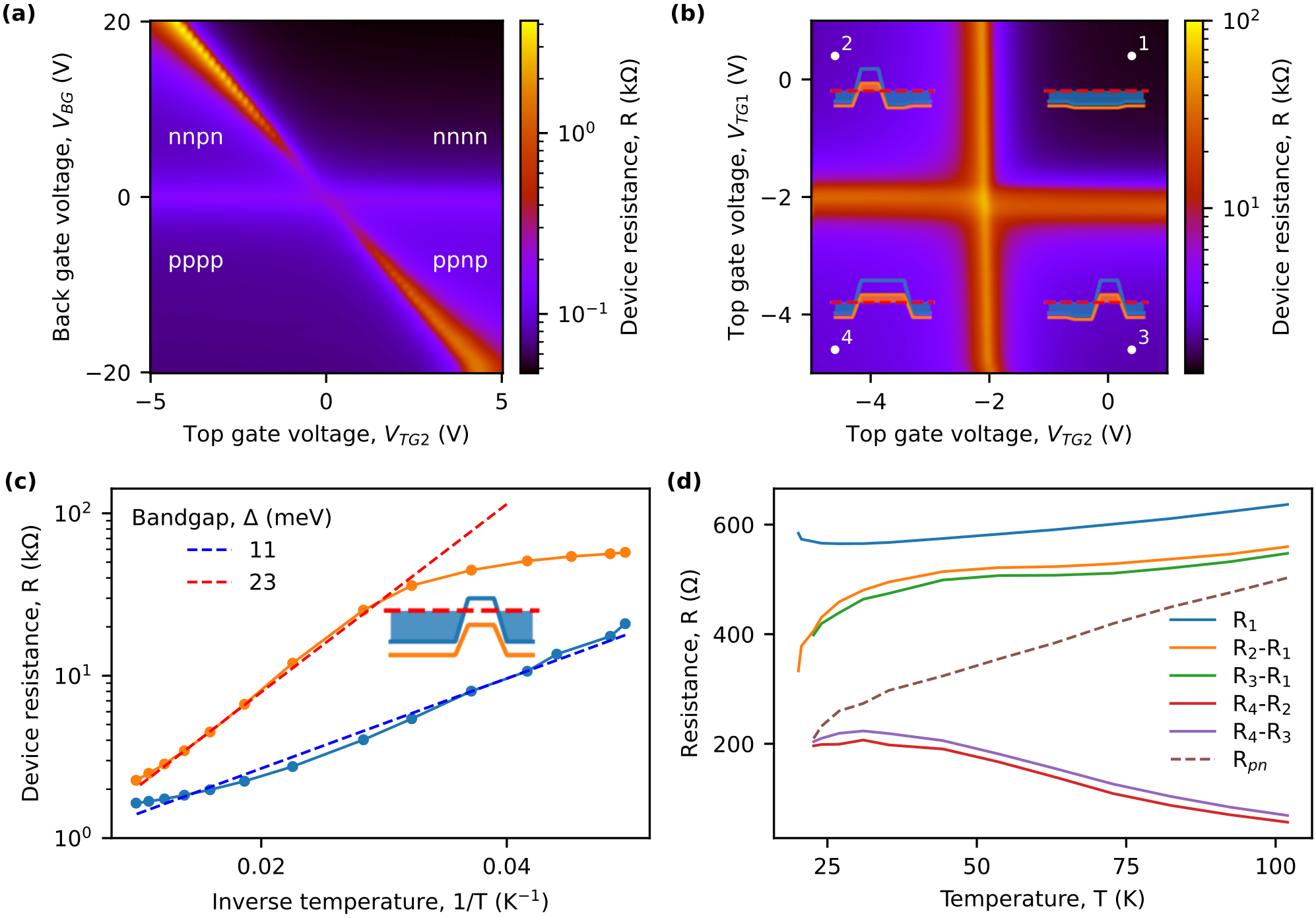
The measured map of two-point resistance vs voltages at the two gates, and , is shown in Fig. 2. In agreement with previous measurements Oostinga_bandgap_opening, Stampfer_AEM_transport_spectroscopy, the maximum resistance is achieved at the map diagonal. Its slope, , determines the ratio of gates’ efficiency, and coincides well with the ratio of the effective thickness of top and bottom dielectrics. Expectantly, the resistance maximum is achieved at largest absolute values of back gate voltages, which is consistent with gap opening in the channel induced by transverse field. A secondary resistance maximum seen at can be attributed to the neutrality condition of regions not covered by the top gate.
A prominent feature of the measured resistance maps is the considerable enhancement of the two-point channel resistance in case when - junctions are induced. To prove the junction-related origin, we classify the four characteristic regions in Fig. 2(a) in accordance with polarity of four characteristic sections in the channel. For example, the notation (top left part of the map) corresponds to -doping of near-contact areas, -doping under the first top gate and -doping under the second one. Only the uniformly doped region have relatively small resistance guaranteed by the absence of the junctions. A similar asymmetry of transfer curves was seen in several Bandurin_EdgeCurrentsShunt, Koppens_Science_VSHE (not all Stampfer_AEM_transport_spectroscopy) previous measurements of BLG, but scarcely attained proper attention gayduchenko_2021. Slightly higher resistance at the -side, may be attributed to electron doping of BLG by Au/Cr contacts.

Further insights into junction effects on net resistance are obtained by sweeping two top gate voltages at fixed value of . An example obtained at V is shown in Fig. 2(b). Clearly, only -doping of both gated regions, identical to doping of near-contact areas, promotes low resistance. Inverting the back gate voltage polarity, one obtains the resistance map with minimal resistance in the left bottom corner (see Supplementary material, Sec. IV). It proves that junctions of interest are formed at the boundary between single- and double-gated regions, but not at the metal-graphene contact.
We further perform temperature-dependent transport measurements providing insights into mechanisms of resistivity. The -dependence of resistance at the charge neutrality point (CNP) follows the Arrhenius law, , where is the bandgap, see Fig. 2(c). The extracted values of at V and V are 11 meV and 23 meV, respectively. These values are in fair agreement with theoretical prediction , where is the gate-channel capacitance per unit area, and eVnm/V Falko_bandgap_theory, yielding and 26 meV, respectively. At the smallest temperatures, K, the resistance tends to saturation indicating the leakages through edge states and/or hopping via defect levels Bandurin_EdgeCurrentsShunt, Oostinga_bandgap_opening.
To single out the effect of - junctions on -dependent resistivity, we further show the -curves for four characteristic configurations with identical absolute values of carrier density in the bulk. These configurations, , , , and , are marked by points 1-4 in Fig. 2(c). Their temperature-dependent resistances are shown in Fig. 2(d). The resistance of uniformly-doped -channel is order of 600 and increases with temperature, which is common for phonon-limited transport. Importantly, the added resistances of non-uniform channel and also grow with temperature. We further extract the -dependent resistivity of a single - junction , which are assumed identical in all regions. The analysis accounts for different bulk conductivities of electrons and holes which can emerge due to different effective masses Band_asymmetry. Under these assumptions, and , which is sufficient for determination of . The result of extraction, shown in Fig. 2(d) with dashed line, again grows with . This lets us conclude that - junctions in BLG have a positive temperature coefficient of resistance (TCR). This contrasts to conventional junctions in Si, Ge, and III-V semiconductors.

Now it is tempting to see whether the measured -dependent resistivity of split-gate BLG device makes any fingerprints on the electro-optical properties. To this end, we measure the device photoconductivity upon illumination with sub-terahertz radiation. During electro-optical measurements, radiation from the sub-THz source (0.13 THz IMPATT diode) was focused to the sample through Si lens glued to the back side of the substrate. Moderate resistivity of substrate (12 cm, B-doped Si) ensured its transparency. A specially designed wideband THz bow-tie antenna mylnikov_2022 was connected to source and drain contacts. The polarization of the light was set along the axis of the bow-tie antenna. The radiation power was chosen so that the device operated in a linear mode, and was 0.5 W (Supplementary material, Sec. V). The photoconductivity was measured using a double-modulation technique: the radiation from sub-THz source was modulated at Hz, the while bias current through the sample oscillated at Hz. The signal measured at difference frequency carries the information about PC.
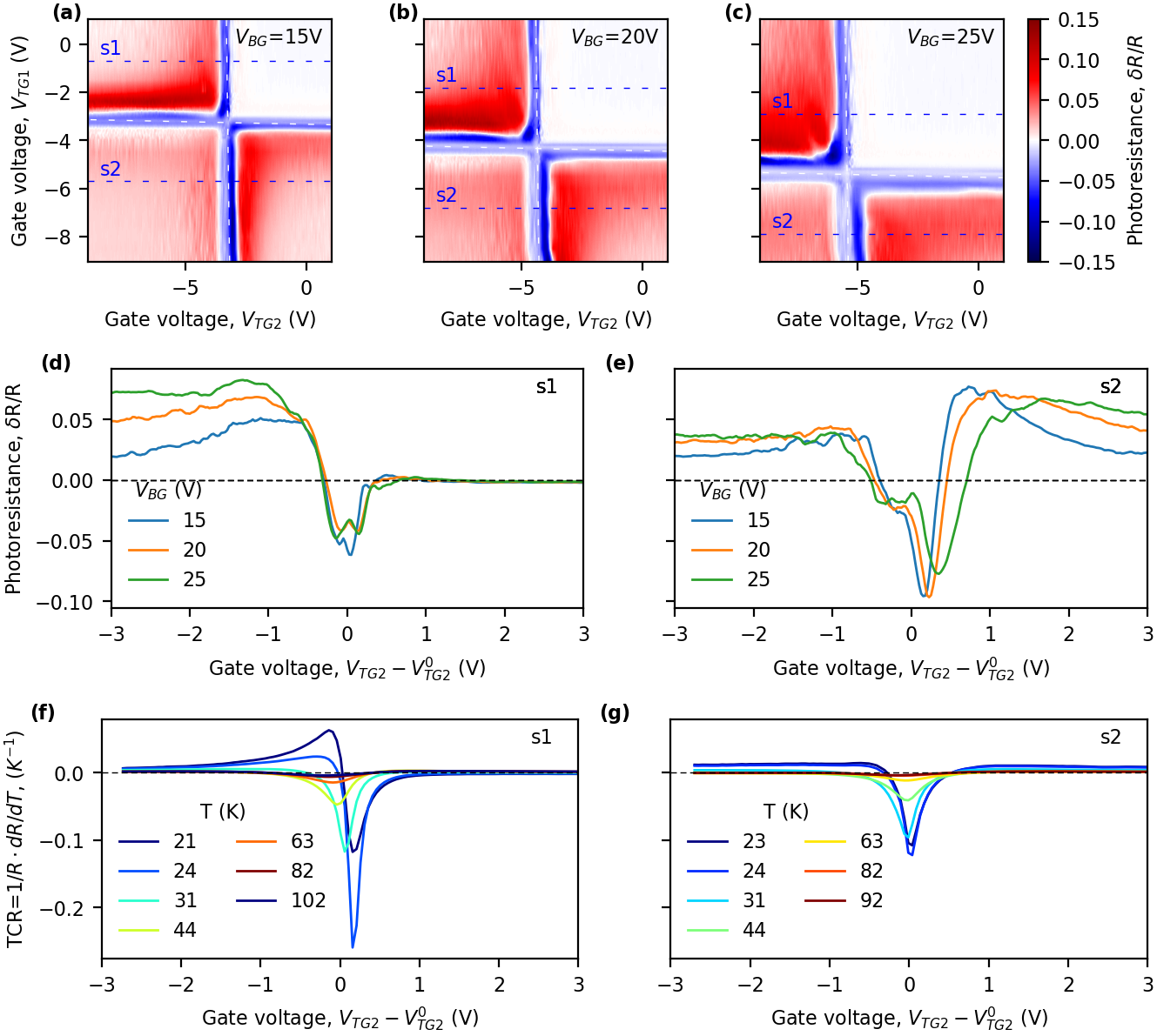
The measured maps of relative photoresistace (PR) are presented in Figs. 3(a)-(c). Its pattern is highly non-trivial, depending on the carrier density in the channel. First, the photoresistance is negative in the vicinity of CNPs under the first and the second gates (marked by white dashed lines). The width of cross-shaped negative photoresistance area grows with increasing the band gap. Second, the photoresistance changes sign abruptly as we shift either of top gate voltages from its CNP. The only exception of this rule occurs if the channel is uniformly doped. In the latest case, the photoresistance signal is very small, so that even its sign cannot be resolved. Nearly-zero signal for uniformly doped channel persists if we invert the back gate voltage (see Supplementary material, Sec. IV).
From the first glance, it may be tempting to explain the observed features of THz PR by the variations of bulk temperature resistance coefficient . Indeed, in the linear regime . As radiation always heats the electrons, , and the sign of photoresistance coincides with that of . The negative PR near the CNP is then readily explained by thermal generation of electrons and holes as the THz radiation heats the charge carriers. The negativity of PR should persist as far as the Fermi level stays within the gap. This fact is reflected in a wider negative PR cross with increasing the back gate voltage (compare Figs. 3(a) and (c)). The positive PR away from CNP is typically explained by phonon-limited transport in the ’metallic state’, where is positive Pump-probe_PC_BLG, Pump-probe-PC-BLG2. However, in our case, this explanation fails. Indeed, this scenario does not explain the asymmetrically vanishing photoresistance for uniformly doped channel.
We now argue that strong positive PR of non-uniformly doped BLG is a consequence of peculiar -dependent resistance of - junctions. To this end, we compare the measured values of and along specific slices and of the full map. The data at slices are shown in panels (d)-(g) of Fig. 3 and cover all four combinations of doping (, , , and ). One observes that positive PR correlates well with positive in the , , and regions away from CNP. The absolute value of in the -region, where junctions are absent, is smaller, and the sign of cannot be unambiguously resolved.

The simultaneous measurements of and at various doping profiles in the channel hint on junction-induced asymmetric photoresistance. Still, the positive sign of PR (and of ) of - junctions in graphene bilayer raises extra questions. Indeed, if the barrier between and sides is overcome by thermally activated carriers, the value of should be negative, as it occurs for conventional semiconductor junctions. Even if the conduction occurs via variable-range hopping through defect levels Oostinga_bandgap_opening or electron-hole puddles Shklovsky_VRH_2d (specific to narrow-gap 2d systems), this should also result in negative TCR.
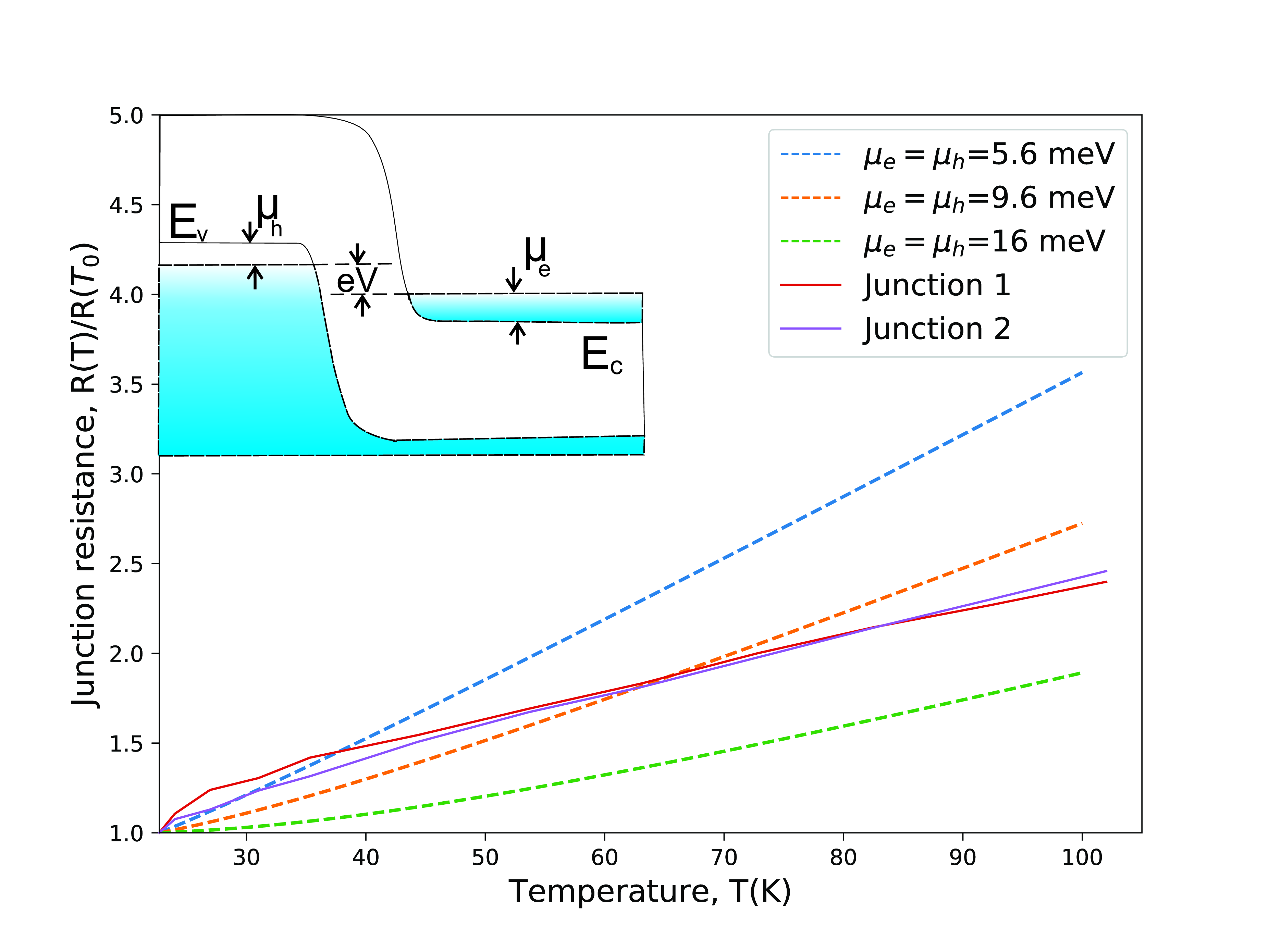
We proceed to show that positive TCR of - BLG junctions can be explained by a simple interband tunneling theory accounting for finite-temperature smearing of the Fermi surface. The relevant band diagram is shown in the inset of Fig. 4. Intuitively, the electrons capable of tunneling are constrained in energy by the edges of conduction and valence bands, in the -region and in the -region. Raising the temperature increases the average kinetic energy of electron and ’pushes’ them away from the tunneling window . Most of thermally activated electrons are now blocked by the gap and do not contribute to transport, and only a small fraction of thermally activated electrons may overcome the barrier.
Direct calculations of tunneling junction conductance based on Esaki theory confirm this idea. Assuming energy-independent tunneling probability and constant densities of states and in the conduction and valence band, we arrive at a remarkably simple formula for -dependent tunneling conductance:
| (1) |
where is the Fermi function, and is the Fermi level (details are in Supplementary material, Sec. VI). The result of theoretical calculations shown in Fig. 4 for various Fermi energies (not known exactly) produces a fair agreement with experiment. Further extension of the model including the energy-dependent density of states in BLG may improve the agreement.
Though the observed dependences of photoresistance on doping can be explained by variations of TCR for the overall FET structure, the variations of THz-induced temperature increase may also play role. Particularly, the presence of extra junction resistances in non-uniformly doped channel may block the cooling of hot electrons via leakage to the contacts Fonf_PRX_Cooling. Simple estimates show that an average increase in electron temperature in the presence of junction resistances is larger than that in uniform channel by a factor of . This fact can also contribute to the observed larger PR in the non-uniform channel, compared to the uniformly doped case.
The measured PC lets us to evaluate the performance of our device acting as a sub-THz bolometer. The power incident on the antenna of 0.8 mm2 area of device #2 is estimated as nW, which accounts for angular divergence of the beam and losses in lenses and intentionally introduced filters (Supplementary material, Sec. V). Under such conditions, the maximum photoresistance reaches . This allows us to estimate the voltage responsivity and noise equivalent power
| (2) |
where is the total voltage noise comprised of Flicker () and Johnson-Nyquist () components. At 34 Hz measurement frequency the measured noise nV/Hz1/2, wich results in pW/Hz1/2. NEP can be further reduced at higher modulation frequencies kHz, where the -noise will surrender to thermal noise. This allows us to estimate the minimum achievable pW/Hz1/2. This is a good value for the bolometric class of photodetectors, it is comparable to low-temperature germanium bolometers low_Ge_1961. The obtained values of and at 25 K are of the same order as in yan_2012 for BLG under IR illumination in terms of external responsivity, but will become superior to reported previously if our device is cooled to the same temperature of 5 K.
In conclusion, our measurements have revealed a strong impact of electrically-induced - junctions in bilayer graphene on its electrical conduction at cryogenic temperatures. Further combined studies of temperature-dependent resistivity and THz photoresitivity have revealed an unexpected increase in junction resistance with increasing . We have shown that this anomaly can be explained with interband tunneling theory taking into account the thermal smearing of the Fermi surface. Instructively, the measured photoresistivity of BLG - junctions is rather high, and leads to quite a large estimate of external responsivity V/W and low of pW/Hz1/2 at K.
The Supporting Information contains following subsections: (I) Device fabrication, (II) Carrier concentration and bandgap in BLG, (III) Carrier mobility extraction, (IV) Device behaviour under inverted back gate, (V) NEP Calculation, (VI) Calculation of the junction tunneling resistance
The work of D.M., E.T., M.K., V.S. and D.S. (sample fabrication, electrical and THz measurements) was supported by the Russian Science Foundation, grant # 21-79-20225. The devices were fabricated using the equipment of the Center of Shared Research Facilities (MIPT). S.Z. acknowledges the support of the the Ministry of Science and Higher Education of the Russian Federation (grant # FSMG-2021-0005). E.T., M.K., I.S., and K.N. thank Vladimir Potanin via Brain and Conscionsness Research Center.
Author declarations
Conflict of interest
The authors have no conflicts of interest to disclose.
Author contributions
D.S. and D.B. conceived the idea of experiment; K.N., D.B., E.T. and M.K. established the technology of sample fabrication at MIPT; M.K. fabricated the samples; D.M. and S.Z. designed the experiment; D.M., E.T., and V.S. performed experimental measurements; D.M. treated the experimental data; I.S. and D.S. developed the theoretical model; D.M., I.S. and D.S. wrote the text. All authors contributed to the discussions of data.
Data availability
Original data are available from the corresponding author upon a reasonable request.