Development of a large-mass, low-threshold detector system with simultaneous measurements of athermal phonons and scintillation light
Abstract
We have combined two low-threshold detector technologies to develop a large-mass, low-threshold detector system that simultaneously measures the athermal phonons in a sapphire detector while an adjacent silicon high-voltage detector detects the scintillation light from the sapphire detector. This detector system could provide event-by-event discrimination between electron and nuclear events due to the difference in their scintillation light yield. While such systems with simultaneous phonon and light detection have been demonstrated earlier with smaller detectors, our system is designed to provide a large detector mass with high amplification for the limited scintillation light. Future work will focus on at least an order of magnitude improvement in the light collection efficiency by having a highly reflective detector housing and custom phonon mask design to maximize light collection by the silicon high-voltage detector.
keywords:
Dark matter , Coherent elastic neutrino-nucleus scattering , Sapphire , Cryogenic phonon detectors , Transition-Edge-Sensors , Machine learning , t-SNE , DBSCAN , light collection , Neganov-Trofimov-Luke gain1 Introduction
Cryogenic detectors have been used in a variety of rare event searches such as Low Mass Dark Matter (LMDM) search [1], Coherent Elastic Neutrino Nucleus Scattering (CENS) [2, 3] and Neutrino-less Double Beta Decay (NDBD) [4] experiments. These experiments look for a nuclear or electron recoil when a WIMP (Weakly Interacting Massive Particle) or a neutrino elastically scatters within the detector. Detection is based on the measurement of basically three types of signals: phonons (heat), scintillation (light) and ionization (charge) [5] caused by the recoil energy transfer. Simultaneous measurement of phonons and charges or phonons and light enhances the capability of these experiments by enabling one to discriminate between different incident particles [6, 7]. The difference in the light yields for electron recoil (ER) and nuclear recoils (NR) can be used to identify these particles as well as to reject background events. The detection of CENS and LMDM requires detectors of large-mass and low-energy thresholds with the ability to discriminate NR and ER events. Among the cryogenic scintillation detectors, sapphire can be a very good option as it can provide low energy thresholds as well as particle identification capability at lower recoil energies. A newly developed sapphire (Al2O3) detector instrumented with Transition-Edge-Sensors (TES) operating at millikelvin temperatures at Texas AM University shows promising results for the detection of low recoil energy events. Because the composite detector material contains Al and O that have lower atomic masses (26 and 16 respectively) than the Si or Ge in semiconductor detectors, the resulting recoil energy from a particle interaction will be larger thereby improving the sensitivity to such interactions. In addition, because the sapphire substrate and the TES both contain Al, the phonon transmission between them is much better than for Si or Ge substrates. The results of the sapphire detector from the test facility shows a baseline resolution of 28.4 0.4 eV using only the phonon channel with no bias voltage applied across the detector [8]. In addition to phonons, a small amount of the deposited energy in the detector is emitted as scintillation light [9]. To detect such small amounts of light would require a very sensitive detector for efficient background discrimination at lower recoil energies.
To address the issue of detecting the scintillation light, our sapphire detector is paired with a phonon-mediated Si detector. To improve the threshold of the Si detector, one can exploit the Neganov Trofimov Luke (NTL) [10, 11] effect in which the detector is operated in a high voltage (HV) mode with an applied bias voltage up to 240V [12]. In this paper, we show the results of the Sapphire-Silicon detector system to detect phonons as well as scintillation light. The expected linearity of the amplified photon signal with the applied voltage is shown.
2 Combined phonon-light measurement
When photons generated by particle interactions in the sapphire detector are absorbed by the Si detector they generate phonons and electron-hole pairs in the Si detector. For example, the light yield of the sapphire detector for 60 keV photons from 241Am is about 10% 3% [9]. The detected signal can be enhanced by applying a bias voltage across the Si detector. The drifting electron-hole pairs in Si create additional phonons leading to an amplification of the phonon signal. The gain due to amplification is the NTL gain, where is the applied voltage across the detector, is the electronic charge and denotes the average energy required to create an electron-hole pair in Si [10, 11]. The NTL gain is directly proportional to the applied voltage .
3 Experimental setup and data set
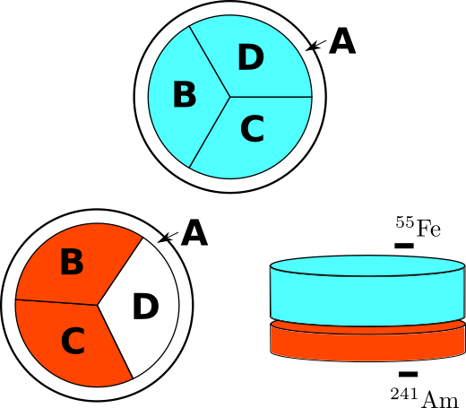
Both sapphire and Si detectors developed by the Texas A&M group have a mass of 100 g. The sapphire detector has a diameter of 76 mm and a thickness of 4 mm, whereas the Si detector has a diameter of 76 mm and a thickness of 10 mm. The sapphire and the Si HV detectors are paired together as a detector module and placed inside a BluFors dilution refrigerator that utilizes cryocoolers to maintain a base temperature of 8 mK. The schematic of the detector module inside the refrigerator is shown in Fig.1 where the sapphire and Si HV detectors are shown in orange and cyan respectively. The detectors are separated by a gap of 2 mm. One face of each detector is covered with TES arrays for phonon signal readout. The sensors are divided into 4 independent groups (A, B, C, D) as shown in the figure where the readout channels are highlighted. To calibrate the Si detector an 55Fe gamma source is placed at the top of the detector surface and an 241Am source (the 5 MeV alpha particles are shielded) is placed at the bottom of the sapphire detector. The light produced in the sapphire is collected in the Si HV detector using coincidence techniques. No reflector has been used in this experimental setup. The Si HV detector is operated with a bias voltage up to 100 V to study the NTL gain of the light output from the sapphire.
4 Analysis and Result
The raw data acquired from the DAQ contains the information of each event in the form of a voltage as a function of time. Because the recorded pulses can be either signal or noise, we describe in the next section an anomaly detection (AD) technique that is used to improve the data quality during pulse filtration in the data analysis.
| Sl. No. | Feature Name | Description | Sl. No. | Feature Name | Description |
|---|---|---|---|---|---|
| 1 | Pre-pulse SD {ch} | Standard deviation of the pulse amplitude for the first 500 s for Sapphire {ch} | 7 | Rise Time {ch} | Time to go from 10 to 90 of the peak amplitude for Sapphire {ch} |
| 2 | Post-pulse SD {ch} | Standard deviation of the pulse amplitude for the last 256 s for Sapphire {ch} | 8 | Fall Time {ch} | Time to go from 90 to 10 of the peak amplitude for Sapphire {ch} |
| 3 | Max Time {ch} | Time of the peak amplitude for Sapphire {ch} | 9 | FW10M {ch} | Full width at 10 of the amplitude for Sapphire {ch} |
| 4 | Min Time {ch} | Time of the minimum amplitude for Sapphire {ch} | 10 | FWHM {ch} | Full width at 50 of the peak amplitude for Sapphire {ch} |
| 5 | Peak {ch} | Peak amplitude for Sapphire {ch} | 11 | FW90M {ch} | Full width at 90 of the peak amplitude for Sapphire {ch} |
| 6 | Max Tail {ch} | Maximum value for the last 256 s for Sapphire {ch} | 12 | Max SD | Standard deviation of time of peak amplitudes among channel B and C |
4.1 Anomaly detection: t-SNE and DBSCAN
Anomaly detection is the identification of events that differ significantly from the majority of the events in the data [13]. In a dataset, AD tries to differentiate between the events on the basis of their similarity/dissimilarity with other events. In this work, we have used a combination of two algorithms to cluster our data, t-SNE [14] and DBSCAN [15] that are used in a sequential manner where the output from t-SNE is used to feed into the DBSCAN algorithm. t-SNE stands for t-distributed stochastic neighborhood embedding. It is used to embed the data from a higher dimensional space to a lower dimension space while keeping similar events together. It is an unsupervised machine learning (ML) technique that understands the overall trends and patterns without any prior knowledge of the data. Density-based spatial clustering of application with noise (DBSCAN) is a clustering method that uses spatial information and groups data based on the relative distance between them. We refer to these groups as clusters. DBSCAN was used instead of other clustering algorithms, as it does not need a predefined number of clusters into which the data has to be divided and it is not constrained by the shape of the clusters.
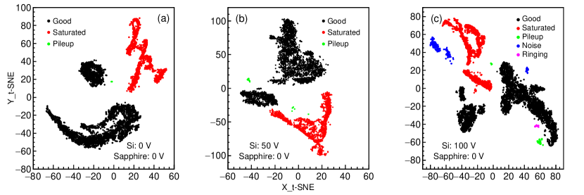
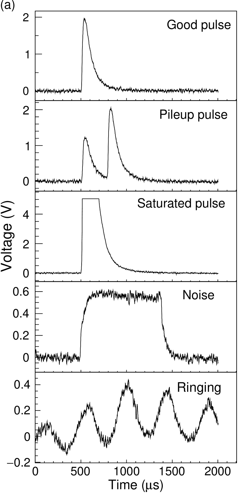
In our analysis, the shape of the pulses from channels B and C of the sapphire detector is characterized by a 23-dimensional vector that we call a feature vector. The description of the feature vector is tabulated in Table 1. An event is any interaction in the detector that triggers a readout. We have only used output from the sapphire TES to characterize the data because the trigger was on the sapphire detector and the pulses from the sapphire detector had a much steeper rise time and fall time than pulses from the Si TES. Using the feature vector we represent each event in 23 dimensions. The Pre-pulse and Post-pulse standard deviation (SD) can help t-SNE to learn about the noisiness of the pulse, while rise and fall times and widths at different amplitudes help to capture the shape of the pulse. The times of maximum and minimum amplitudes depend on the trigger and any anomalous event that might deviate from the dataset on these variables. The last variable, Max SD, characterizes the range of time the detector took to detect the pulse in different channels. We expect the times to be slightly different but not very far away from each other. This information is used to embed the 23-dimension feature vector into a 2-dimensional space using t-SNE. After this, we cluster the data in the 2-dimensional space using DBSCAN. Fig.2 shows different clusters in the 2-dimensional t-SNE space using the data from three different bias voltages across the Si detector. We now examine the different clusters that result from DBSCAN and group clusters that correspond to saturated pulses, good pulses, piled-up pulses, ringing, and noise. There can be multiple clusters with good pulses, for example at 0 V there were two clusters with good pulses. These clusters contained pulses with different amplitude ranges. We did not need such classification and hence labeled both clusters as good pulses. These clusters are shown in different colors in Fig.2. Good pulses are shown in black, saturated pulses in red, pile-ups in green, noise in blue, and ringing in magenta. Examples of a typical good pulse, pile-up pulse, saturated pulse, noise, and ringing are shown in Fig.3(a). Events from the cluster which represent good pulses are filtered out for further analysis.
Traditionally the way to filter bad pulses from good pulses is by making use of a pulse template. One generates a pure pulse template from the unfiltered data itself. This template is fitted on the pulse and a cut is used to filter good pulses. In an unsupervised machine learning algorithm such as the one proposed above, we do not need to provide any information for the filtration other than the dataset itself. Our feature vector tries to understand the shape of the pulses and represents them as a vector and t-SNE converts this to a 2-dimensional space while keeping events similar in shape together. DBSCAN is then used to group these events based on their density. However, in the pulse template fit method filtration is based on the template which is created by a human based on his judgment from an unfiltered dataset. We measured the efficiency and purity of our proposed method by creating a labeled dataset of images. We extracted nine events with good pulses, nine with saturated pulses, nine with piled-up pulses, three with noise pulses, and three with ringing pulses from our dataset. Then a new dataset with 6008 events was created by linearly combining these events within their types and labeled. There were 1993 good pulses in the new dataset. After applying t-SNE and DBSCAN to the dataset we obtained twenty clusters. Clusters that contained mostly good pulses were filtered out. The purity of the filtered pulses was 98.1. Out of 1993 good pulses, 1990 were filtered out and we missed 3 pulses that give us an efficiency of 99.8. This accuracy was obtained on a labeled subset of the full analysis dataset. We expect a similarly high accuracy when applying this pulse selection method on the full dataset.
4.2 Processing raw data after filtering: Optimal filter (OF) method
We have used pulse template fitting algorithm known as Optimal filter (OF) algorithm [16] to extract energy information from the raw traces of the filtered data set. Noise power spectral density (PSD) with few noise pulses is calculated from the dataset taken with random triggers. The OF algorithm is then applied to the raw data set where the pulses are fitted with the template in the frequency domain to determine the pulse amplitude from the best fit values. The amplitude measured in the OF method is directly proportional to the energy of the pulses. The OF amplitude distribution can then be calibrated using known energy sources. Similarly, the random triggered data set which is the measure of the noise can be used to calculate the baseline resolution of the detectors.
4.3 Calibration of Si detector
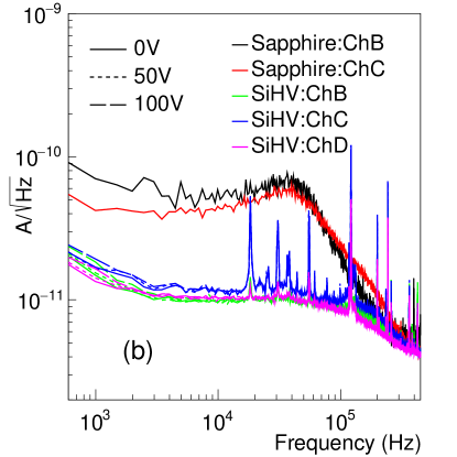
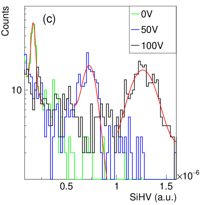
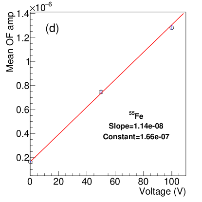
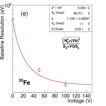
Si HV detector is calibrated with 6 keV gammas from the 55Fe source. The data was taken with the bias voltage at 0 V, 50 and 100 V. Fig.3(b) shows the noise performance of the sapphire channels and the Si channels when the Si HV detector was biased at 0 V, 50 V and 100 V. The noise in the Si channels does appear to increase with increasing bias voltage applied to the Si HV detector. Fig.3(c) shows the 6 keV peak from the 55Fe source measured at the three bias voltages and fitted with a gaussian. The mean value of the distribution is plotted at different voltages and shown in Fig.3(d). As expected the NTL amplification of the 6 keV events is linearly proportional to the applied voltages as shown by the straight line in the figure. The baseline resolution was calculated using random triggered data for all three voltages. Fig.3(e) shows the baseline resolution as a function of the voltage where the lowest baseline resolution achieved is 12 eV.
4.4 Amplification of light in Si detector
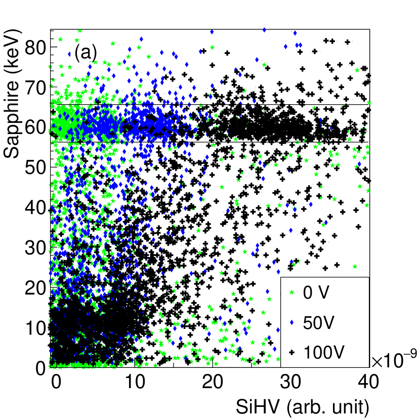
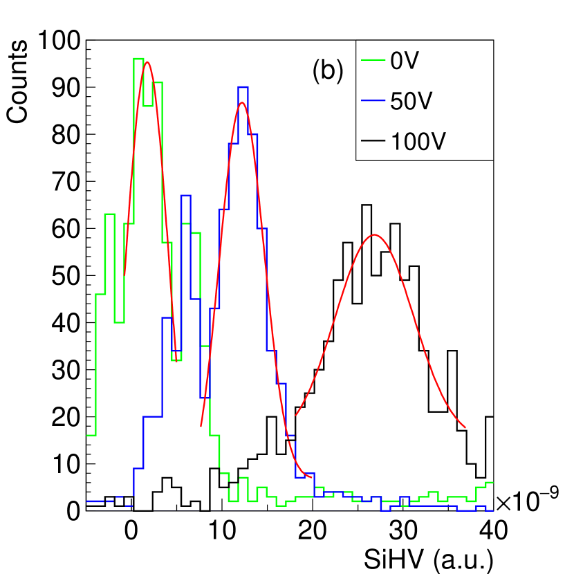
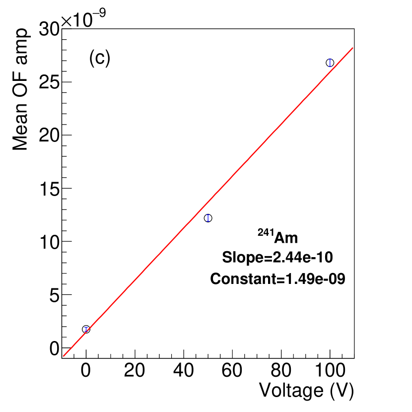
In this section, we discuss the amplification of the signal in the Si HV detector due to the scintillation light from the sapphire detector by examining only coincident events in the sapphire and Si detectors. An 241Am source is used to illuminate the sapphire detector with 60 keV gammas. When a 60 keV gamma is absorbed in the sapphire, both phonons and scintillation light are created. On average only 10% of the energy of the incident gamma is converted into light [9]. The phonons are measured by the TES on the sapphire detector whereas only the photons that reach the Si HV detector are detected by the TES on the Si detector. A Monte Carlo simulation to estimate the geometric efficiency in collecting the photons by the Si HV detector indicated that only 40% of the photons reach the Si detector. Moreover, the high voltage phonon mask on the Si HV detector facing the sapphire detector covers 90% of the surface, further reducing the light from entering the Si detector. Finally given the reflectivity of Si to be 56% [17, 18], we expect that the effective light collection to be only 2%. The scintillation photons of 6 keV (10 of 60 keV gammas) total energy (after undergoing losses from solid angle acceptance and absorption) will hit the Si detector and create phonon signals in Si. The amplification of the light signal in the Si detector is observed through coincidence events with the sapphire detector. The correlation between the sapphire and Si detectors is shown in Fig.4(a) where we see that light output from the 60 keV events in sapphire gets amplified in the Si detector with the applied voltages. Fig.4(b) shows the projection of 60 keV events in the Si detector which demonstrate the amplification of the light at different voltages. The measured light in the Si HV detector is converted to energy by multiplying the calibration factor of the detector. The amount of light we measure in our detector is 2% which matches well with the expected number after considering all the losses. To show the linear relationship we have plotted the mean of the projected event distribution with the respective voltages. Fig.4(c) shows the linearity of the amplified light output in the Si detector.
5 Conclusion and outlook
In this paper, we demonstrate the simultaneous detection of phonons and scintillation light in a system composed of a sapphire and Si HV detector. Despite using any reflector in the experiment, we are able to measure 2% of the total light produced in the sapphire which agrees well with the expected value after considering all the losses. The lowest energy threshold achieved in the Si HV detector is 36 eV (3 times the baseline resolution) at 100 V. As the Si HV detector can be operated at voltages up to 240 V, our future work aims to further lower the energy threshold by applying higher voltages. We will also focus on improving the light collection efficiency by having a reflective detector housing and a Si HV detector with a custom phonon mask design that covers less area of the Si HV detector surface for maximum light collection efficiency. We can conclude that this type of detector system can be used in the search for low-mass dark matter and CENS where low energy recoils can be detected with active background discrimination.
Acknowledgement
This work was supported by the U. S. Department of Energy (DOE) under Grant Nos DE-SC0020097, DE-SC0018981, DE-SC0017859, and DE-SC0021051. We acknowledge the seed funding provided by the Mitchell Institute for early conceptual and prototype development. We would like to acknowledge the support of DAE-India through the project Research in Basic Sciences - Dark Matter and SERB-DST-India through the J. C. Bose Fellowship.
References
- [1] C. Tao, Dark matter searches: an overview, Journal of Instrumentation 15 (06) (2020) C06054–C06054.
- [2] D. Z. Freedman, Coherent effects of a weak neutral current, Phys. Rev. D 9 (1974) 1389–1392.
- [3] J. Barranco, O. G. Miranda, T. I. Rashba, Probing new physics with coherent neutrino scattering off nuclei, Journal of High Energy Physics 2005 (12) (2005) 021–021.
- [4] A. Zolotarova, Bolometric Double Beta Decay Experiments: Review and Prospects, Symmetry 13 (12) (2021) 2255.
- [5] R. Essig, G. K. Giovanetti, N. Kurinsky, D. McKinsey, K. Ramanathan, K. Stifter, T.-T. Yu, Snowmass2021 Cosmic Frontier: The landscape of low-threshold dark matter direct detection in the next decade, in: 2022 Snowmass Summer Study, 2022. arXiv:2203.08297.
-
[6]
M. Bravin, M. Bruckmayer, T. Frank, S. Giordano, M. Loidl, O. Meier,
P. Meunier, D. Pergolesi, F. Pröbst, W. Seidel, M. Sisti, P. di Stefano,
L. Stodolsky, S. Uchaikin, L. Zerle,
Simultaneous
measurement of phonons and scintillation light for active background
rejection in the cresst experiment, Nuclear Instruments and Methods in
Physics Research Section A: Accelerators, Spectrometers, Detectors and
Associated Equipment 444 (1) (2000) 323–326.
doi:https://doi.org/10.1016/S0168-9002(99)01371-6.
URL https://www.sciencedirect.com/science/article/pii/S0168900299013716 - [7] G. Angloher, et al., NUCLEUS: cryogenic calorimeters to detect coherent nuclear scattering of reactor antineutrinos, PoS ICHEP2022 (2022) 589. doi:10.22323/1.414.0589.
-
[8]
S. Verma, S. Maludze, M. Lee, M. Chaudhuri, V. Iyer, V. Kashyap, A. Kubik,
Y.-T. Lin, R. Mahapatra, N. Mirabolfathi, N. Mishra, B. Mohanty, H. Neog,
A. Jastram, M. Platt,
Low-threshold
sapphire detector for rare event searches, Nuclear Instruments and Methods
in Physics Research Section A: Accelerators, Spectrometers, Detectors and
Associated Equipment (2022) 167634doi:https://doi.org/10.1016/j.nima.2022.167634.
URL https://www.sciencedirect.com/science/article/pii/S0168900222009263 -
[9]
J. Amaré, B. Beltrán, S. Cebrián, E. García, H. Gómez, I. G. Irastorza,
G. Luzón, M. Martínez, J. Morales, A. O. de Solórzano, C. Pobes,
J. Puimedón, A. Rodríguez, J. Ruz, M. L. Sarsa, L. Torres, J. A. Villar,
N. Coron, G. Dambier, J. Leblanc, P. de Marcillac, T. Redon,
Light yield of undoped sapphire at
low temperature under particle excitation, Applied Physics Letters 87 (26)
(2005) 264102.
arXiv:https://doi.org/10.1063/1.2158518, doi:10.1063/1.2158518.
URL https://doi.org/10.1063/1.2158518 - [10] B. Neganov, V. Trofimov, Colorimetric method measuring ionizing radiation, Otkryt. Izobret 146 (215) (1985) 53.
-
[11]
P. N. Luke, Voltage‐assisted
calorimetric ionization detector, Journal of Applied Physics 64 (12) (1988)
6858–6860.
arXiv:https://doi.org/10.1063/1.341976, doi:10.1063/1.341976.
URL https://doi.org/10.1063/1.341976 -
[12]
V. Iyer, N. Mirabolfathi, G. Agnolet, H. Chen, A. Jastram, F. Kadribasic,
V. Kashyap, A. Kubik, M. Lee, R. Mahapatra, B. Mohanty, H. Neog, M. Platt,
Large
mass single electron resolution detector for dark matter and neutrino elastic
interaction searches, Nuclear Instruments and Methods in Physics Research
Section A: Accelerators, Spectrometers, Detectors and Associated Equipment
1010 (2021) 165489.
doi:https://doi.org/10.1016/j.nima.2021.165489.
URL https://www.sciencedirect.com/science/article/pii/S0168900221004745 -
[13]
A. Zimek, E. Schubert,
Outlier detection,
in: Encyclopedia of Database Systems, Springer New York, 2017, pp. 1–5.
doi:10.1007/978-1-4899-7993-3_80719-1.
URL https://doi.org/10.1007/978-1-4899-7993-3_80719-1 -
[14]
L. van der Maaten, G. Hinton,
Visualizing data
using t-SNE, Journal of Machine Learning Research 9 (2008) 2579–2605.
URL http://www.jmlr.org/papers/v9/vandermaaten08a.html -
[15]
M. Ester, H.-P. Kriegel, J. Sander, X. Xu,
A density-based
algorithm for discovering clusters in large spatial databases with noise,
AAAI (1996).
URL https://www.aaai.org/Papers/KDD/1996/KDD96-037.pdf -
[16]
F. Caleb, W. Sam,
qetpy
documentation (oct 2021).
URL https://readthedocs.org/projects/qetpy/downloads/pdf/latest/ -
[17]
M. A. Green,
Self-consistent
optical parameters of intrinsic silicon at 300k including temperature
coefficients, Solar Energy Materials and Solar Cells 92 (11) (2008)
1305–1310.
doi:https://doi.org/10.1016/j.solmat.2008.06.009.
URL https://www.sciencedirect.com/science/article/pii/S0927024808002158 -
[18]
M. A. Green, M. J. Keevers,
Optical
properties of intrinsic silicon at 300 k, Progress in Photovoltaics:
Research and Applications 3 (3) (1995) 189–192.
arXiv:https://onlinelibrary.wiley.com/doi/pdf/10.1002/pip.4670030303,
doi:https://doi.org/10.1002/pip.4670030303.
URL https://onlinelibrary.wiley.com/doi/abs/10.1002/pip.4670030303