Non-charge-transfer origin of Enhancement in a Surface Superconductor Si(111)-()-In with Adsorbed Organic Molecules
Abstract
The effects of adsorption of Zn-phthalocyanine (ZnPc) molecules on the superconductivity of the Si(111)-()-In surface are studied through transport measurements under ultrahigh vacuum environment. The ZnPc molecules are found to increase the transition temperature by 11% at maximum, which is about 2.7 times the increase previously reported using CuPc. By contrast, angle-resolved photoemission spectroscopy measurements and ab initio calculations show that charge transfer from the In atomic layers to ZnPc is substantially smaller than that to CuPc. This clearly shows that charge transfer should be excluded as the origin of the increase in . The push-back effect induced by physical adsorption of molecules is discussed as a possible mechanism for the enhancement.
Recently, two-dimensional (2D) superconductors with atomic-scale thickness and high crystallinity have been discovered and attracted much attention [1, 2, 3, 4, 5, 6, 7, 8, 9]. One of the important characteristics of such atomic-layer superconductors is their sensitivity to surfaces and interfaces. For example, in a single-layer FeSe grown on a substrate, the superconducting transition temperature () rises from the bulk value of 8 K to over 40 K, due to the effect of carrier doping from the substrate or alkali metals [10, 11, 12]. In addition, superconductivity can be induced at the interfaces of insulating compounds and in twisted bilayer graphene by carrier doping using gate electrodes[5, 13, 7].
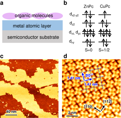
Regarding metal atomic layers epitaxially grown on semiconductor surfaces [1, 2, 3, 14, 15], carrier doping with a gate-electrode is not straightforward because the atomic layer structure would easily be destroyed at the interface. However, by utilizing the weak van der Waals-like interaction between organic molecules and metal surfaces, an ideal interface can be realized (Fig. 1(a)). Recently, adsorption of Cu-phthalocyanine (CuPc) molecule was reported to increase the of a surface superconductor Si(111)-()-In (referred to as ()-In) by up to about 4% [16]. In this system, charges corresponding to 1.6 electrons per molecule are transferred from In atoms to CuPc molecules, and the increase in was ascribed to this “hole doping”. However, similar experiments using molecule resulted in a decrease in although a larger hole doping is expected due to its strong acceptor character [17]. As exemplified by this, the mechanism for modulation in atomic-layer superconductors with adsorbed organic molecule has not been fully clarified yet.
In the present study, we assemble ZnPc molecular layers on Si(111)-()-In and measure the change in by transport measurements. The adsorption of ZnPc molecules increases by up to 11%, which is about 2.7 times the corresponding value reported for CuPc. By contrast, the charge transfer from the In atomic layers to ZnPc is found to be significantly smaller than that to CuPc by angle-resolved photoemission spectroscopy (ARPES) measurements and ab initio calculations. This clearly shows that charge transfer is not the origin of the observed increase in in this system. We discuss that the rise observed here may be attributed to the push-back effect, which is commonly observed for surface adsorption of organic molecule .
The surface superconductor ()-In consists of double atomic layers of bulk In(001) planes epitaxially grown on a Si(111) substrate, where a lattice mismatch leads to formation of a superstructure [18, 19, 20, 21, 22]. A pristine ()-In undergoes a superconducting transition at K [2, 3, 14, 23, 24]. In this study, ZnPc was adopted as the adsorbed organic molecule. ZnPc has a structure in which a metal ion is coordinated to the center of the phthalocyanine framework [25]. Since it has an electronic configuration similar to that of CuPc where is coordinated to the center (Fig. 1(b)), their comparison should be insightful. After flash-cleaning of a Si(111) substrate at 1250 in an ultrahigh vacuum (UHV) environment ( Pa), In was deposited and the sample was annealed around 300. This routinely leads to the formation of a ()-In surface. The surface structure and crystallinity of the prepared sample were characterized through low-energy electron diffraction (LEED) and scanning tunneling microscopy (STM) at room temperature. ZnPc (purity ) was deposited on the sample from a crucible by resistive heating. The ZnPc coverage was estimated with a quartz crystal microbalance and was further checked with STM. Here, one monolayer (ML) is defined as the coverage of the molecular layer fully covering the surface.
Transport measurements were carried out to determine the superconducting transition temperature of the sample. The temperature dependence of the sample resistance was acquired by the four-terminal method using a home-built UHV-compatible cryostat [3, 23, 26, 27]. A non-doped Si wafer (resistivity cm) was used as the substrate to avoid an leak current at low temperatures. After the ()-In surface was prepared, the current path and electrode area were defined with sputtering through a shadow mask [23, 27], which enables quantitative transport measurements. The sample was cooled to 1.7 K by liquid helium pumping. First, the resistance of the pristine ()-In was measured. ZnPc layers with a sub-ML coverage was then grown on the same sample and the measurement was taken again; this process was repeated until the coverage reached 1.5 ML. Separately, STM and ARPES measurements were conducted at low temperatures to investigate the molecular assembly structure and the charge transfer due to ZnPc adsorption, respectively. A highly doped n-type Si wafer () was used for the former, while a moderately doped n-type Si wafer () was used for the latter. The amount of the charge transfer and spin magnetic moment in the molecule were also obtained by ab initio calculations, and the density of states (DOS) of ()-In near the Fermi level was also calculated [28].
Figure 1(c) shows the STM image of ZnPc layers ( ML) grown on the ()-In surface. The ZnPc layers consist of 1 ML-thick islands with their edges extending along two orthogonal directions. The growth of molecules follows the layer-by-layer mode at least up to 2 ML coverage. Fig. 1(d) shows a representative STM image of a ZnPc layer taken with the molecular resolution. The black arrows indicate the and directions of the Si lattice. These directions were determined by measuring the atomic image of ()-In. The ZnPc lattice has a unit cell of a square and its principal axes are rotated by 45∘ with respect to the and directions. This structure is identical to that of CuPc layers on the ()-In surface reported previously [16]. This observation suggests that ZnPc forms an epitaxial molecular film due to a lattice matching to ()-In as in the case of CuPc.
Transport measurements were carried out to investigate the effect of ZnPc coverage on the of ()-In. Figure 2(a) plots the temperature dependence of the sheet resistance (i.e., 2D resistivity) observed for different coverages of ZnPc. They all exhibit a steep drop at low temperatures due to the superconducting transition. The figure also shows the results of fitting based on thermal fluctuation theories of 2D superconductivity [23, 29]. The fitting range was taken to be , where is defined as measured at 4.5 K. For the pristine sample ( ML), K was obtained (solid circles). was found to increase with increasing coverage of ZnPc, reaching the maximal value of K at a coverage of ML (open squares). showed a decreasing trend for ML, resulting in K at ML (solid triangles). We note that, while the resistive transition is very sharp for ML, its width becomes broadened for ML. Accordingly, the experimental data exhibit noticeable deviations from the fitting curves for . This suggests that the adsorption of ZnPc molecules induces a spatial inhomogeneity of and that the determined here is close to the maximal value.
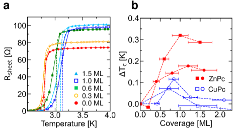
Figure 2(b) displays defined as a variation in ( acquired for two different ZnPc/()-In samples (solid circles/squares). The two plots follow the qualitatively same behavior. amounts to K at maximum, corresponding to about 11% of of ()-In. Figure 2(b) also plots induced by CuPc adsorption (open circles/squares) [16]. also peaks around ML but only reaches K at maximum. Thus, the maximum value of for ZnPc is about 2.7 times larger than that for CuPc. In the previous work[16], the increase in was attributed to charge transfer from the In to the molecular layer (i.e., hole doping). If this interpretation is correct, ZnPc should cause a larger charge transfer than CuPc.
To estimate the amount of charge transfer from ZnPc molecule, the change of the Fermi surface of ()-In was studied through ARPES measurements. Figure 3(a) shows the result for a pristine ()-In surface. The color (brightness) of the figure indicates photoelectron intensity, and the axes correspond to the and directions, respectively. The Fermi surface consists of two arc-like structures enclosed by the dahsed lines and butterfly-like structures in between, which agree well with the previous reports [19, 16, 30, 31, 27]. Figure 3(b) shows the result for the ()-In surface covered with ML-thick ZnPc layer. The Fermi surface of ()-In is still clearly visible, while the background of photoelectron intensity increases. This strongly suggests that the atomic structure of ()-In is preserved under the ZnPc layer and that there exist no strong chemical bonds between ZnPc and In atoms. Notably, as shown in Figs. 3(c) and 3(d), the peak positions of momentum distribution curves (MDCs) are shifted only slightly. These arc-like structures are the consequence of back-folding of the circular 2D Fermi surface, which originates from the In conduction electrons [19]. If holes are doped into ()-In by ZnPc adsorption as expected, the radius of the original Fermi surface shrinks. This in turn leads to a decrease in the distance between the two arc-like structures [16, 30]. Our result described above contradicts this scenario.
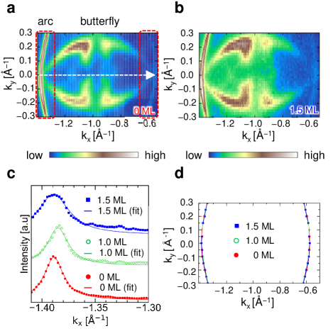
The amount of charge transfer due to the molecule adsorption is evaluated as follows. The maximal peak shifts is detected for ML coverages of ZnPc. This leads to a charge transfer per molecule , where is the elementary charge (here, the negative sign of corresponds to electron transfer from the In layers to the molecules.) Meanwhile, the analogous ARPES measurements revealed that the radius of the ()-In Fermi surface shrank by when 1.0 ML-thick CuPc was adsorbed instead of ZnPc [30]. This leads to as a charge transfer due to CuPc adsorption [32]. We also carried out ab initio calculations to quantify the charge transfer due to ZnPc. The result is , which is only 47% of the value previously obtained for CuPc with the same method [16]. Table 1 summarizes the maximal values of obtained by transport measurements and the amount of charge transfer deduced from the ARPES measurements and the ab initio calculations. Both ARPES and ab initio calculations show that ZnPc induces less charge transfer than CuPc, which is opposite to the expected trend based on the variations in [33]. Therefore, we conclude that the increase in is not attributable to charge transfer between the molecules and the In atoms.
| physical quantity | method | ZnPc | CuPc |
|---|---|---|---|
| (K) | transport | 0 | |
| ARPES | |||
| ab initio calc. |
At present, the mechanism of the enhancement is not clear. We first note that the emergence of unconventional superconductivity, which is caused by a strong electron correlation as in high- cuprates, is very unlikely since the system can be described by a one-electron band picture [27, 31]. This idea is supported by the observation of the s-wave like superconducting energy gap reported previously [24]. Here we propose the push-back effect as a possible origin based on the standard Bardeen-Cooper-Schrieffer (BCS) theory. Since the potential barrier for electrons at the metal surface is finite in height, the wavefunctions of conduction electrons penetrate into the vacuum region. However, when organic molecules are physically adsorbed on the surface, the conduction electrons are pushed back toward the metal nuclei by Pauli repulsion because of overlapping with the molecular wavefunctions. This is called the push-back effect (or the Pauli repulsion effect) [34, 35, 36]. In particular, phthalocyanine molecules adsorbed in the planar configuration are expected to cause a strong effect, because their -conjugated orbitals extends perpendicular to the surface. This should enhance both the electron DOS per unit volume and the attractive interactions between electrons through an increase in electron-phonon interactions. According to the BCS theory, is expressed by the following formula [37]
| (1) |
where is the Debye phonon frequency, is the DOS per unit volume at the Fermi level , and is the attractive potential between electrons. Therefore, is expected to rise when increases due to the push-back effect. Using the typical value for BCS superconductors, an increase in by 2% enhances by 10%. Thus, this mechanism is considered realistic. We note that variations based on an analogous mechanism has been predicted for the superconductivity of monolayer graphite intercalation compounds [38].
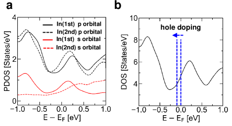
Since the push-back effect is a universal phenomenon caused by physically adsorbed organic molecules, it is expected to appear commonly for ZnPc and CuPc. Then, what is the cause of the difference in induced by these molecules? According to Park et al.[20, 39], the DOS of ()-In is an increasing function of the energy near the Fermi level . Therefore, a hole doping should lead to a decrease in and consequently to an decrease in . Since the hole doping effect is larger for CuPc than for ZnPc, the decrease is more significant for CuPc. To further check this idea, we independently performed ab initio calculations for ()-In to obtain the projected DOS (PDOS) for individual atomic orbitals. Figures 4(a) and 4(b) show the calculated PDOS, where the former refers to the DOS projected onto the orbitals of In atoms in the first (top) and second (bottom) layers and the latter to the summation of individual contributions. Since all of them are increasing functions of near , the above argument should to be applicable irrespective of the degree of contribution of each orbital to superconductivity.
Finally, we consider the possibility that localized spins in ZnPc and CuPc, if exist, may suppress superconductivity [16, 40]. As depicted in Fig. 1(b), ZnPc has no total spin in the isolated state. Our ab initio calculations confirmed that spin magnetic moment is equal to (: Bohr magneton) even after adsorption on the ()-In surface. By contrast, CuPc has a total spin in the isolated state and retains after adsorption on ()-In. Nevertheless, the magnetic moment induced in the In atomic layer is [16]. This means that there is no exchange interaction between the spins of CuPc and those of conduction electrons in the In layer. This is because the orbital accommodating the spins of CuPc hardly overlaps with the wavefunctions of the In atoms due to its planar form. Therefore, the effect of localized spins on superconductivity can be neglected for both ZnPc and CuPc.
In summary, we have clarified that the charge transfer between organic molecules and In atoms should be excluded as the origin of the enhancement in ()-In. On the contrary, the charge transfer is likely to lower . While the origin of the increase in this surface system is not clear at present, we have proposed the push-back effect due to the organic molecules as a plausible mechanism. The present study may provide an important clue for understanding the modulations, which have been observed in many kinds of surface/interface 2D superconductors.
The financial support from the following is acknowledged: JSPS Kakenhi Grant No. 22H01961, 20H05621, 20H02707, and World Premier International Research Center (WPI) Initiative on Materials Nanoarchitectonics (T. U.), JSPS Kakenhi Grant No. 22H01957, 19H02592, and the Spintronics Research Network of Japan (Spin-RNJ) (K. S).
References
- [1] S. Y. Qin, J. Kim, Q. Niu, and C. K. Shih: Science 324 (2009) 1314.
- [2] T. Zhang, P. Cheng, W. J. Li, Y. J. Sun, G. Wang, X. G. Zhu, K. He, L. L. Wang, X. C. Ma, X. Chen, Y. Y. Wang, Y. Liu, H. Q. Lin, J. F. Jia, and Q. K. Xue: Nat. Phys. 6 (2010) 104.
- [3] T. Uchihashi, P. Mishra, M. Aono, and T. Nakayama: Phys. Rev. Lett. 107 (2011) 207001.
- [4] Q.-Y. Wang, Z. Li, W.-H. Zhang, Z.-C. Zhang, J.-S. Zhang, W. Li, H. Ding, Y.-B. Ou, P. Deng, K. Chang, J. Wen, C.-L. Song, K. He, J.-F. Jia, S.-H. Ji, Y.-Y. Wang, L.-L. Wang, X. Chen, X.-C. Ma, and Q.-K. Xue: Chin. Phys. Lett. 29 (2012) 037402.
- [5] J. T. Ye, Y. J. Zhang, R. Akashi, M. S. Bahramy, R. Arita, and Y. Iwasa: Science 338 (2012) 1193.
- [6] S. Ichinokura, K. Sugawara, A. Takayama, T. Takahashi, and S. Hasegawa: ACS Nano 10 (2016) 2761.
- [7] Y. Cao, V. Fatemi, S. Fang, K. Watanabe, T. Taniguchi, E. Kaxiras, and P. Jarillo-Herrero: Nature 556 (2018) 43.
- [8] Y. Yu, L. Ma, P. Cai, R. Zhong, C. Ye, J. Shen, G. D. Gu, X. H. Chen, and Y. Zhang: Nature 575 (2019) 156.
- [9] T. Uchihashi: Supercond. Sci. Technol. 30 (2017) 013002.
- [10] S. He, J. He, W. Zhang, L. Zhao, D. Liu, X. Liu, D. Mou, Y.-B. Ou, Q.-Y. Wang, Z. Li, L. Wang, Y. Peng, Y. Liu, C. Chen, L. Yu, G. Liu, X. Dong, J. Zhang, C. Chen, Z. Xu, X. Chen, X. Ma, Q. Xue, and X. J. Zhou: Nat. Mater. 12 (2013) 605.
- [11] J. F. Ge, Z. L. Liu, C. Liu, C. L. Gao, D. Qian, Q. K. Xue, Y. Liu, and J. F. Jia: Nat. Mater. 14 (2014) 285.
- [12] Y. Miyata, K. Nakayama, K. Sugawara, T. Sato, and T. Takahashi: Nat. Mater. 14 (2015) 775.
- [13] Y. Saito, Y. Kasahara, J. Ye, Y. Iwasa, and T. Nojima: Science 350 (2015) 409.
- [14] M. Yamada, T. Hirahara, and S. Hasegawa: Phys. Rev. Lett. 110 (2013) 237001.
- [15] F. Ming, S. Johnston, D. Mulugeta, T. Smith, P. Vilmercati, G. Lee, T. Maier, P. Snijders, and H. Weitering: Phys. Rev. Lett. 119 (2017) 266802.
- [16] S. Yoshizawa, E. Minamitani, S. Vijayaraghavan, P. Mishra, Y. Takagi, T. Yokoyama, H. Oba, J. Nitta, K. Sakamoto, S. Watanabe, T. Nakayama, and T. Uchihashi: Nano Lett. 17 (2017) 2287.
- [17] N. Sumi, Y. Yamada, M. Sasaki, R. Arafune, N. Takagi, S. Yoshizawa, and T. Uchihashi: The Journal of Physical Chemistry C 123 (2019) 8951.
- [18] J. Kraft, S. L. Surnev, and F. P. Netzer: Surface Science 340 (1995) 36.
- [19] E. Rotenberg, H. Koh, K. Rossnagel, H. Yeom, J. Schäfer, B. Krenzer, M. Rocha, and S. Kevan: Phys. Rev. Lett. 91 (2003) 246404.
- [20] J. Park and M. Kang: Phys. Rev. Lett. 109 (2012) 166102.
- [21] K. Uchida and A. Oshiyama: Phys. Rev. B 87 (2013) 165433.
- [22] T. Shirasawa, S. Yoshizawa, T. Takahashi, and T. Uchihashi: Phys. Rev. B 99 (2019) 100502(R).
- [23] T. Uchihashi, P. Mishra, and T. Nakayama: Nanoscale Res. Lett. 8 (2013) 167.
- [24] S. Yoshizawa, H. Kim, T. Kawakami, Y. Nagai, T. Nakayama, X. Hu, Y. Hasegawa, and T. Uchihashi: Phys. Rev. Lett. 113 (2014) 247004.
- [25] M.-S. Liao and S. Scheiner: J. Chem. Phys. 114 (2001) 9780.
- [26] S. Yoshizawa and T. Uchihashi: J. Phys. Soc. Jap. 83 (2014) 065001.
- [27] S. Yoshizawa, T. Kobayashi, Y. Nakata, K. Yaji, K. Yokota, F. Komori, S. Shin, K. Sakamoto, and T. Uchihashi: Nat. Commun. 12 (2021) 1462.
- [28] (Supplemental material 1) The detail of the calculation methods is provided online.
- [29] (Supplemental material 2) The detail of the fitting process is provided online.
- [30] R. Sagehashi, T. Kobayashi, T. Uchihashi, and K. Sakamoto: Surface Science 705 (2021) 121777.
- [31] T. Kobayashi, Y. Nakata, K. Yaji, T. Shishidou, D. Agterberg, S. Yoshizawa, F. Komori, S. Shin, M. Weinert, T. Uchihashi, and K. Sakamoto: Phys. Rev. Lett. 125 (2020) 176401.
- [32] (Supplemental material 3) The detail of the charge transfer estimation is provided online.
- [33] The samples used in the transport and ARPES experiments should have the same carrier densities in the In layers despite the different dopant levels in the Si substrates. This is supported by the fact that the radius of the Fermi surface of ()-In obtained with a high-doped Si wafer ()[31] is equal to that obtained in the present study () within the experimental error.
- [34] P. S. Bagus, V. Staemmler, and C. Wöll: Phys. Rev. Lett. 89 (2002) 096104.
- [35] G. Witte, S. Lukas, P. S. Bagus, and C. Wöll: Appl. Phys. Lett. 87 (2005) 263502.
- [36] K. Toyoda, I. Hamada, K. Lee, S. Yanagisawa, and Y. Morikawa: J. Chem. Phys. 132 (2010) 134703.
- [37] M. Tinkham: Introduction to Superconductivity (McGraw-Hill, New York, 1996) 2nd ed.
- [38] G. Profeta, M. Calandra, and F. Mauri: Nat. Phys. 8 (2012) 131.
- [39] J. W. Park and M. H. Kang: Phys. Rev. B 92 (2015) 045306.
- [40] T. Uchihashi, S. Yoshizawa, E. Minamitani, S. Watanabe, Y. Takagi, and T. Yokoyama: Mol. Syst. Des. Eng. 4 (2019) 511.