Department: Head \editorEditor: Name, xxxx@email
TCN-CUTIE: A 1036 TOp/s/W, 2.72 µJ/Inference, 12.2 mW All-Digital Ternary Accelerator in 22 nm FDX Technology
Abstract
Tiny Machine Learning (TinyML) applications impose µJ/Inference constraints, with a maximum power consumption of tens of mW. It is extremely challenging to meet these requirements at a reasonable accuracy level. This work addresses the challenge with a flexible, fully digital Ternary Neural Network (TNN) accelerator in a RISC-V-based System-on-Chip (SoC). Besides supporting Ternary Convolutional Neural Networks, we introduce extensions to the accelerator design that enable the processing of time-dilated Temporal Convolutional Neural Networks (TCNs). The design achieves 5.5 µJ/Inference, 12.2 mW, 8000 Inferences/sec at 0.5 V for a Dynamic Vision Sensor (DVS) based TCN, and an accuracy of 94.5% and 2.72 µJ/Inference, 12.2 mW, 3200 Inferences/sec at 0.5 V for a non-trivial 9-layer, 96 channels-per-layer convolutional network with CIFAR-10 accuracy of 86%. The peak energy efficiency is 1036 TOp/s/W, outperforming the state-of-the-art silicon-proven TinyML quantized accelerators by 1.67x while achieving competitive accuracy.
1 Introduction
Advances in Machine Learning (ML) research in recent years have enabled a new direction of research within the field of embedded systems, called TinyML, targeting the execution of non-trivial ML tasks within the strict constraints of low-power (mW) embedded devices. TinyML is becoming increasingly pervasive with applications including wearable computer vision, gesture recognition, and many more. The key challenges in TinyML are energy efficiency at a few mW of power while ensuring accurate and fast inference. Specialized TinyML accelerators tackle both challenges by providing high throughput at low power, but often they do so by compromising accuracy or by specializing on a single network topology, with no flexibility. We present a flexible and accurate TinyML architecture, integrating CUTIE, a highly configurable Ternary Neural Network (TNN) accelerator based on a fully unrolled compute architecture [1] within the Kraken RISC-V System-on-Chip (SoC). Further, we introduce a novel Temporal Convolutional Network (TCN) extension within the CUTIE architecture, enabling the execution of autonomous data-to-label time series prediction, a very common use case for TinyML devices. We present the deployment and power measurements of a neural network architecture exploiting these extensions, which achieves an accuracy of 94.5% at an energy cost of per inference, performing gesture recognition from a Dynamic Vision Sensor (DVS) trained on the DVS 128 dataset [2]. To the best of our knowledge, we are the first to demonstrate a peak core energy efficiency beyond for neural network inference in an all-digital and flexible platform, measured on a fabricated SoC.
2 SoC Implementation
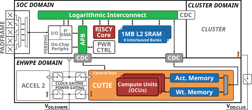
The Kraken SoC is a RISC-V-based microcontroller based on the Pulpissimo SoC [3]. A RI5CY core [4] serves as the fabric controller (FC), coordinating the operation of the other subsystems. For parallel signal processing tasks, it contains an 8-core PULP cluster of RISC-V cores. Kraken has an extensive set of peripherals for off-chip communication. They are implemented as µDMA [5] extensions, freeing the FC from most management duties. On-chip peripherals include an event unit for interrupt mapping, a RISC-V-compliant debug unit for JTAG control of the chip and a power controller. 4 Frequency-Locked Loop (FLL) modules provide independently run-time configurable clocks to the µDMA peripherals, the SoC domain, the accelerator (EHWPE) domain, and the PULP cluster. Kraken has three core supply rails and four core power domains. The SoC, cluster and EHWPE domains each have a separate supply. Kraken features task-specific accelerators: In the following sections, we focus on the TNN inference engine, its integration, and silicon measurements. The accelerators share their supply voltage, but each is located in its power domain and can be power-gated individually to minimize current draw by idle system components. A block diagram of the SoC architecture is shown in Figure 1.
3 CUTIE Design
The Completely Unrolled Ternary Inference Engine (CUTIE), is a highly configurable Convolutional Neural Network (CNN) accelerator architecture for completely ternarized neural networks, introduced in [1]. In contrast to systolic arrays, CUTIE uses a completely unrolled compute architecture, which means that one Output Channel Compute Unit (OCU) is allocated for every output channel, making the computation output-stationary. Further, each OCU includes weight buffers, minimizing weight data movement. Each OCU processes a full activation window per cycle, without pipelining in the compute units, making the architecture also input-stationary. To fully exploit all opportunities for data reuse in CNNs, a linebuffer designed to eliminate data access stalling is added. Thanks to this highly parallel design, CUTIE fully exploits data reuse at all levels and minimizes data movement. In addition, ternary weights and activations enable the exploitation of zero values to translate sparsity into reduced toggling in the compute units. Thus, minimized data movement and switching activity are the cornerstones of CUTIE’s efficiency.
In this work, we extend the CUTIE TNN accelerator to support hybrid 2D-CNN & 1D-TCN networks. As demonstrated in [6], the combination of low precision, i.e. ternarized, CNN and TCN achieved superior accuracy in classifying time-distributed data like streams of events produced by event-based sensors, like DVS cameras. Data produced by such sensors are characterized by a high level of unstructured sparsity and exhibit both short and long temporal dynamics. A hybrid CNN-TCN approach allows fine-tuning the network capabilities to achieve the highest accuracy when processing event streams. Specifically, the CNN captures the spatial dependency among neighboring events, that cluster in specific regions of the input feature map, as well as short temporal dependency among events belonging to consecutive time steps; an event happening in the scene tends to persist over multiple time steps. The 1D TCN extracts longer temporal dependencies among features distributed across the entire sample time window. 1D-TCNs use dilated convolutions [7], meaning feature map data is accessed in a strided fashion. The extensions required to support 1D-TCNs efficiently are twofold: 1) We designed a TCN memory, enabling dilated feature map data access without stalling, 2) We implemented a scheduling algorithm that maps 1D dilated convolutions to 2D undilated convolutions, which make use of CUTIE’s efficient compute architecture.
4 TCN Extensions
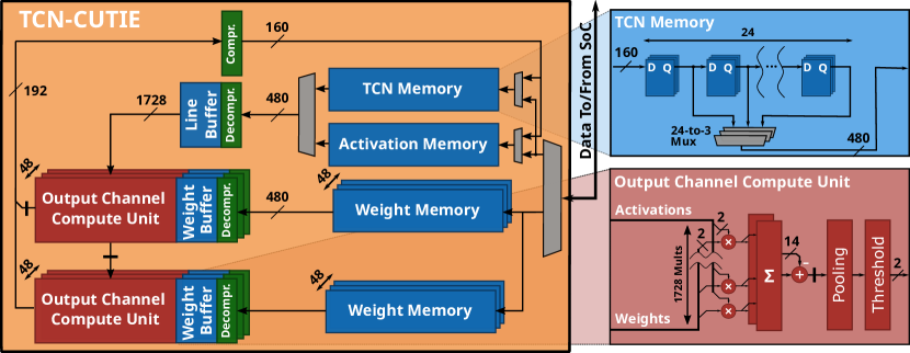
To support hybrid 2D-CNN & 1D-TCN networks, CUTIE has to be extended with a small memory, the TCN memory, that can hold the 1D feature vectors that are extracted by each inference of a 2D-CNN. The TCN memory enables the execution of hybrid 2D-CNN & 1D-TCN networks, as well as pure 1D processing. The output of the TCN memory has the same size as the activation memory, which is achieved by multiplexing three time steps according to the address of the first required pixel. In the Kraken SoC, the TCN memory was dimensioned to hold a total of 24 feature vectors, corresponding to a memory size of only 576 bytes. Nevertheless, 24 time steps are sufficient to cover a long receptive window even at high framerates: if the 2D CNN takes as input 15 stacked frames captured at a rate of 300 FPS ( the speed of most ordinary cameras), the resulting receptive time window for a TCN covering 24 time steps is still . Due to its small size, we implemented the TCN memory/ as a flip-flop-based shift register to reduce leakage power. A block diagram of the CUTIE TNN accelerator with the proposed TCN memory extension is shown in Figure 2.
The second extension we introduce to the CUTIE accelerator is the mapping of 1D dilated convolutions. Dilated 1D convolutions with a kernel length and dilation factor of an input with a kernel can be described by their mathematical definition, shown in Equation 1:
| (1) |
where
is the causally padded input vector x. The main advantage of dilated convolutions over undilated ones lies in their ability to reach a longer receptive field in fewer layers. In a TCN with and , where denotes the -th layer’s kernel dilation, the receptive field in layer can be calculated as
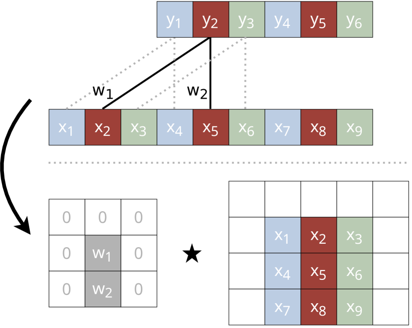
. The receptive field increases exponentially with the number of layers, decreasing the number of layers needed to cover a given number of input steps. For the 24 input steps supported by TCN-CUTIE, the number of layers is reduced from 12 for undilated convolutions to 5 with exponentially increasing dilations. In a direct implementation , the elements of are not accessed contiguously, instead, they are accessed with a stride of . Due to the specialized memory hierarchy of CUTIE, non-contiguous or strided accesses lead to stalling, decreasing efficiency. To avoid this, we reformulate equation 1 as a 2D correlation:
where
A visual representation of this mapping is shown in Figure 3. To form the dense 2D feature map, the 1D vector is wrapped around after D elements. Further, zero padding (shown in white in Figure 3) is applied on the edges to implement the causality required by TCNs as well as the correct start- and endpoint of the convolution. To respect the hardware constraints of CUTIE, i.e. weight kernels having size 3×3, the 1D weight kernel is projected into the middle column of the 2D weight kernel, while all other elements in the weight kernels are set to zero. This mapping ensures that the kernel dot product is only computed over a single column and the column elements are dilated by the dilation factor D. Since this mapping is fully equivalent to a 2D convolutional layer and all transforms necessary can be computed offline and require no data marshalling, it fully and efficiently reuses the CUTIE architecture with minor hardware overhead.
5 TCN-CUTIE Implementation
Thanks to its highly configurable nature, the CUTIE architecture can be adapted to many application scenarios. In the Kraken SoC, we dimensioned the memories for feature map sizes of up to 6464 pixels with up to 96 channels. We designed the TCN memory to hold a total of 24 time steps. Since CUTIE’s throughput per cycle is enormous due to the high degree of parallelism, we used relaxed timing constraints during synthesis, to enable extensive instantiation of low-leakage library cells. The CUTIE TNN accelerator’s clock can be hierarchically clock-gated to minimize idle switching activity in idle OCUs when network layers have a small number of output channels. Inference can be triggered via a configuration register or an interrupt line from I/O peripherals, enabling autonomous data preparation and inference without intervention from the FC. After inference has concluded, CUTIE asserts an interrupt which is used to wake up the FC.
6 Kraken Physical implementation
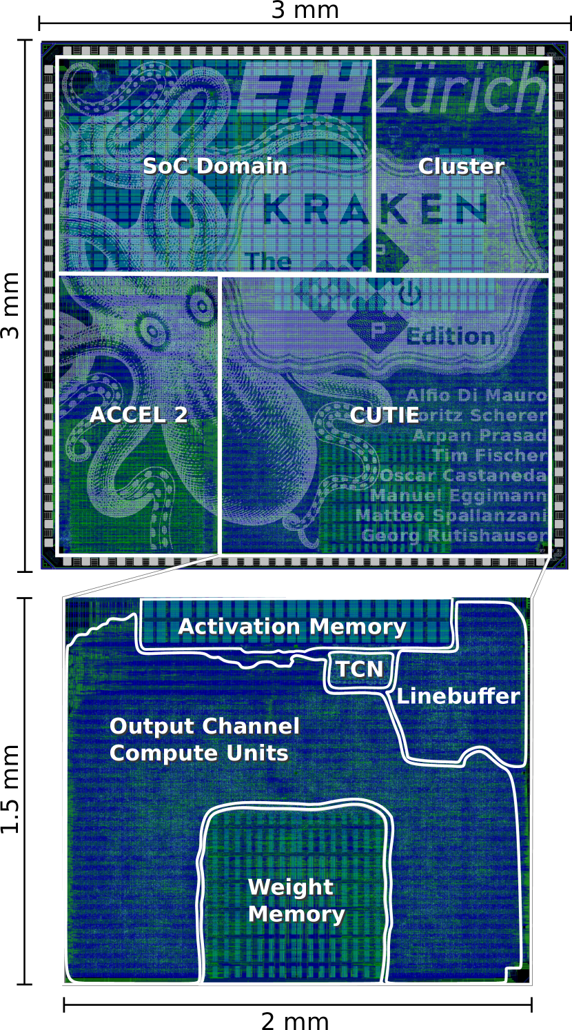
The Kraken chip has been designed and manufactured in GlobalFoundries 22nm technology, the total die area is . The three Kraken subsystems are implemented as independent clock and power domains. Both the general-purpose RISC-V-based accelerator and the EHWPE domain can be entirely power-gated to reduce their leakage consumption when not in use. The chip can operate in a wide supply voltage range, i.e., from . The chip host a total of 88 pads, 46 of which can be used either as GPIO or as an alternate function, i.e., as one of the signals of each IO peripherals, in an all-to-all muxing scheme. Figure 4 shows an annotated floorplan of the Kraken SoC, including the SoC Domain, Cluster, Accelerator 2, as well as CUTIE. The CUTIE accelerator occupies of area. In the CUTIE layout, the area occupied by memory macros composing the internal buffers, and digital logic are highlighted. The memories including weight buffers in the OCUs take up 60% of the total die area of CUTIE, while the rest is used by the compute units. The additional TCN memory which holds the sequence samples was implemented in Standard Cell Memory (SCM) and has a negligible impact of less than 1% on area.
7 Evaluation
To benchmark the accelerator’s performance against similar state-of-the-art designs, we measure the execution of a ternarized 9-layer (8 CONV layers, 1 FC classifier) CIFAR-10 network as used in [1, 8, 9] with 96 instead of 128 channels. This network achieves an accuracy of 86% on CIFAR-10, which is on par with the binarized version using 128 layers used in [9, 8]. Similarly, we execute the hybrid 2D-CNN & 1D-TCN network proposed in [6], consisting of 5 2D-CNN layers and 4 1D-TCN layers that process 5 time steps. This network achieves an accuracy of 94.5% on the 12-class DVS 128 dataset.
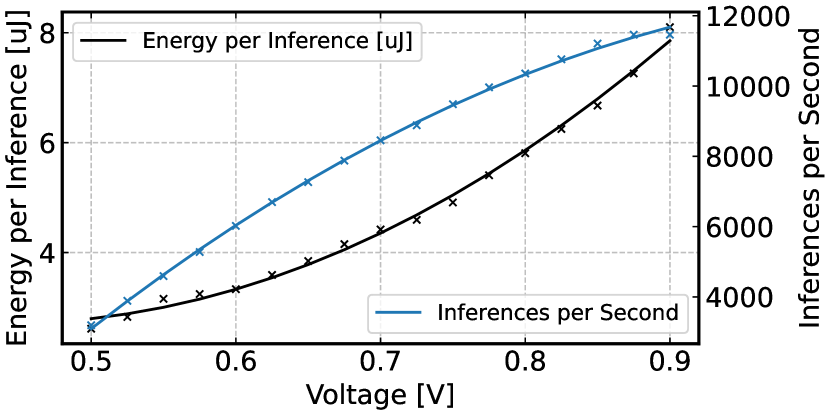
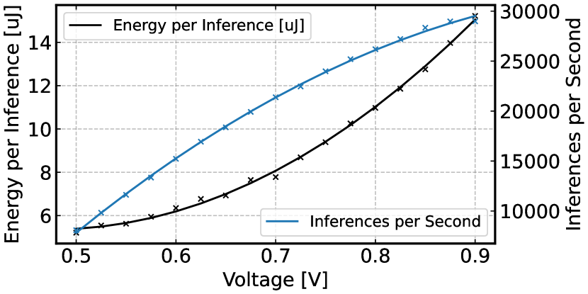
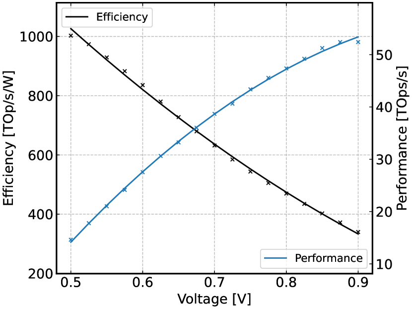
To evaluate the power consumption of CUTIE, we measured the current drawn by the Kraken ASIC on an ASIC tester, while running the deployed networks on CUTIE using pre-selected inputs which were randomly drawn from the respective validation set of the datasets used for training. The presented power consumption numbers of the CUTIE accelerator include its memories, but do not include chip I/O energy. All measurements were performed at room temperature. We profiled the accelerator’s performance at 25C over a range of - . Below , the integrated SRAM macros start exhibiting bit errors. In terms of efficiency, we find that the operating corner, operating at achieves the lowest energy per inference of and at an average throughput of and for the CIFAR-10 and DVS networks, with a peak energy efficiency in the first layer of the CIFAR-10 network of and peak throughput of . The operating corner using achieves the highest peak throughput of , but a lower peak energy efficiency of . Figure 5 shows plots for throughput and energy per inference against voltage for the CIFAR-10 and DVS networks. Figure 6 shows the peak energy efficiency per operation and throughput versus voltage for the first layer of the CIFAR-10 network.
8 Comparison with State-of-the-Art
| Characteristics | [9] | [8] | This work | ||||
|---|---|---|---|---|---|---|---|
| Computation Method | digital | digital | digital | ||||
| Weight Precision | binary | binary | ternary | ||||
| Activation Precision | binary | binary | ternary | ||||
| Technology | |||||||
| Dataset | CIFAR-10 | CIFAR-10 | CIFAR-10 | ||||
| Accuracy | 86% | 86% | 86% | ||||
| Energy per Inference | |||||||
| Core Area [] | 1.4 | 0.39 | 2.96 | ||||
| Voltage [V] | 0.65 | 0.37 | 0.75 | 0.5 | 0.9 | ||
| Throughput [TOp/s] | 2.8 | 3.4 | 163 | 16 | 56 | ||
| Peak Core Energy Efficiency [TOp/s/W] | 230 | 617 | 269 | 1036 | 446 | ||
Table 1 shows a comparison of CUTIE on the Kraken SoC with state-of-the-art highly quantized digital convolutional network accelerators. CUTIE achieves a peak throughput of and a peak energy efficiency of , surpassing the highest reported efficiency in the literature: a Binary Neural Network (BNN) accelerator manufactured in a more advanced technology node [8]. As demonstrated in [1] by the use of post-layout simulation of a larger configuration of CUTIE, the high energy efficiency of CUTIE can be explained mainly by two design characteristics: The source of CUTIE’s efficiency is the minimization of data movement, which limits the efficiency of comparable accelerators. This is achieved by the fully unrolled architecture, which minimizes the number of accesses to each data item. Secondly, the simple ternary processing elements and the use of very wide addition trees leverages sparsity in ternary data indirectly. This is shown in [1], where ternarized networks with very sparse activations and weights reduce the inference energy cost on CUTIE by 36%. In this work, we improve on these characteristics by optimizations in the front- and backend design flow, as well as using a smaller CUTIE configuration.
To evaluate our TCN extensions we compare our design with traditional TCN accelerators, as well as with Spiking Neural Network (SNN) accelerators, which purportedly are more energy efficient for sparse, event-based time-series data like DVS.
Although there are no standard benchmarks or datasets for TCNs, we can compare the average energy efficiency over an inference for state-of-the-art designs. In [10], the authors propose a TCN accelerator design for continuous, ultra-low-power keyword spotting. While running 64 inferences of a network per second, they achieve an average power consumption between and , leading to average energy efficiency of to , measured by post-synthesis simulation. In direct comparison, our measured average energy cost per operation on the DVS network is around 5 - 15 lower.
Even when comparing the performance of the TCN extensions with state-of-the-art SNN accelerators on the DVS 128 dataset, our implementation meets the best reported accuracy using TNNs in literature, a network deployed on the IBM Truenorth platform, which achieves a statistical accuracy of 94.6%, just 0.1% better than our ternary TCN, while requiring 3250 more energy per inference [2] than our design.
When comparing with a modern Intel accelerator implementation, the measured energy per inference of beats the best reported energy efficiency on a similar DVS and EMG dataset, an SNN running on the Intel Loihi platform and achieving an accuracy of 96.0%, by a factor of 63.4 [11].
9 Conclusion
We presented the CUTIE implementation in the Kraken SoC and evaluated its performance. By exploiting minimized data movement and switching activity coupled with aggressive voltage scaling, we achieve a peak efficiency of , surpassing the SoA in ultra-low-energy CNN inference by a factor of . Similarly, the implemented TCN extensions are demonstrated to surpass the energy efficiency of the state-of-the-art by a factor of 5.
Acknowledgement
The authors would like to thank armasuisse Science & Technology for funding this research, and IniVation for kindly lending us a DVS Camera.
References
- [1] M. Scherer, G. Rutishauser, L. Cavigelli, and L. Benini, “CUTIE: Beyond PetaOp/s/W Ternary DNN Inference Acceleration With Better-Than-Binary Energy Efficiency,” IEEE Transactions on Computer-Aided Design of Integrated Circuits and Systems, vol. 41, no. 4, pp. 1020–1033, Apr. 2022, conference Name: IEEE Transactions on Computer-Aided Design of Integrated Circuits and Systems.
- [2] A. Amir, B. Taba, D. Berg, T. Melano, J. McKinstry, C. Di Nolfo, T. Nayak, A. Andreopoulos, G. Garreau, M. Mendoza, J. Kusnitz, M. Debole, S. Esser, T. Delbruck, M. Flickner, and D. Modha, “A Low Power, Fully Event-Based Gesture Recognition System,” in 2017 IEEE Conference on Computer Vision and Pattern Recognition (CVPR), Jul. 2017, pp. 7388–7397, iSSN: 1063-6919.
- [3] P. D. Schiavone, D. Rossi, A. Pullini, A. Di Mauro, F. Conti, and L. Benini, “Quentin: an Ultra-Low-Power PULPissimo SoC in 22nm FDX,” in 2018 IEEE SOI-3D-Subthreshold Microelectronics Technology Unified Conference (S3S), Oct. 2018, pp. 1–3, iSSN: 2573-5926.
- [4] M. Gautschi, P. D. Schiavone, A. Traber, I. Loi, A. Pullini, D. Rossi, E. Flamand, F. K. Gürkaynak, and L. Benini, “Near-Threshold RISC-V Core With DSP Extensions for Scalable IoT Endpoint Devices,” IEEE Transactions on Very Large Scale Integration (VLSI) Systems, vol. 25, no. 10, pp. 2700–2713, Oct. 2017, conference Name: IEEE Transactions on Very Large Scale Integration (VLSI) Systems.
- [5] A. Pullini, D. Rossi, G. Haugou, and L. Benini, “uDMA: An autonomous I/O subsystem for IoT end-nodes,” in 2017 27th International Symposium on Power and Timing Modeling, Optimization and Simulation (PATMOS), Sep. 2017, pp. 1–8.
- [6] G. Rutishauser, M. Scherer, T. Fischer, and L. Benini, “Ternarized TCN for uJ/inference gesture recognition from DVS event frames,” in Proceedings of the 2022 Conference & Exhibition on Design, Automation & Test in Europe, ser. DATE ’22. Leuven, BEL: European Design and Automation Association, Mar. 2022, pp. 736–741.
- [7] C. Lea, M. D. Flynn, R. Vidal, A. Reiter, and G. D. Hager, “Temporal Convolutional Networks for Action Segmentation and Detection,” arXiv, Tech. Rep. arXiv:1611.05267, Nov. 2016, arXiv:1611.05267 [cs] type: article. [Online]. Available: http://arxiv.org/abs/1611.05267
- [8] P. C. Knag, G. K. Chen, H. E. Sumbul, R. Kumar, M. A. Anders, H. Kaul, S. K. Hsu, A. Agarwal, M. Kar, S. Kim, and R. K. Krishnamurthy, “A 617 TOPS/W All Digital Binary Neural Network Accelerator in 10nm FinFET CMOS,” in 2020 IEEE Symposium on VLSI Circuits, Jun. 2020, pp. 1–2, iSSN: 2158-5636.
- [9] B. Moons, D. Bankman, L. Yang, B. Murmann, and M. Verhelst, “BinarEye: An always-on energy-accuracy-scalable binary CNN processor with all memory on chip in 28nm CMOS,” in 2018 IEEE Custom Integrated Circuits Conference (CICC), Apr. 2018, pp. 1–4, iSSN: 2152-3630.
- [10] J. S. P. Giraldo, V. Jain, and M. Verhelst, “Efficient Execution of Temporal Convolutional Networks for Embedded Keyword Spotting,” IEEE Transactions on Very Large Scale Integration (VLSI) Systems, vol. 29, no. 12, pp. 2220–2228, Dec. 2021, conference Name: IEEE Transactions on Very Large Scale Integration (VLSI) Systems.
- [11] E. Ceolini, C. Frenkel, S. B. Shrestha, G. Taverni, L. Khacef, M. Payvand, and E. Donati, “Hand-Gesture Recognition Based on EMG and Event-Based Camera Sensor Fusion: A Benchmark in Neuromorphic Computing,” Frontiers in Neuroscience, vol. 14, 2020. [Online]. Available: https://www.frontiersin.org/article/10.3389/fnins.2020.00637
Moritz Scherer received the B.Sc. and M.Sc. degree in electrical engineering and information technology from ETH Zürich in 2018 and 2020, respectively, where he is currently pursuing a Ph.D. degree at the Integrated Systems Laboratory. Contact him at scheremo@iis.ee.ethz.ch. {IEEEbiographynophoto}Alfio Di Mauro received the M.Sc. degree in electronic engineering from the Electronics and Telecommunications Department (DET), Politecnico di Torino, in 2016. He is currently pursuing a Ph.D. degree with the Integrated System Laboratory (IIS), ETH Zürich. Contact him at adimauro@iis.ee.ethz.ch. {IEEEbiographynophoto}Tim Fischer received the B.Sc. and M.Sc. degree in electrical engineering and information technology from ETH Zürich in 2018 and 2021, respectively, where he is currently pursuing a Ph.D. degree at the Integrated Systems Laboratory. Contact him at fischeti@iis.ee.ethz.ch. {IEEEbiographynophoto}Georg Rutishauser received his B.Sc. and M.Sc.degrees in Electrical Engineering and Information Technology from ETH Zürich in 2015 and 2018, respectively. He is currently pursuing a Ph.D. degree at the Integrated Systems Laboratory at ETH Zürich. Contact him at georgr@iis.ee.ethz.ch. {IEEEbiographynophoto}Luca Benini holds the Chair of Digital Circuits and Systems at ETH Zürich and is a Full Professor with the Universita di Bologna. He is a Fellow of the ACM and the IEEE and a member of the Academia Europaea. Contact him at lbenini@iis.ee.ethz.ch.