Strong gate-tunability of flat bands in bilayer graphene due to moiré encapsulation between hBN monolayers
Abstract
When using hexagonal boron-nitride (hBN) as a substrate for graphene, the resulting moiré pattern creates secondary Dirac points. By encapsulating a multilayer graphene within aligned hBN sheets the controlled moiré stacking may offer even richer benefits. Using advanced tight-binding simulations on atomistically-relaxed heterostructures, here we show that the gap at the secondary Dirac point can be opened in selected moiré-stacking configurations, and is independent of any additional vertical gating of the heterostructure. On the other hand, gating can broadly tune the gap at the principal Dirac point, and may thereby strongly compress the first moiré mini-band in width against the moiré-induced gap at the secondary Dirac point. We reveal that in hBN-encapsulated bilayer graphene this novel mechanism can lead to isolated bands flatter than 10 meV under moderate gating, hence presenting a convenient pathway towards electronically-controlled strongly-correlated states on demand.
I Introduction
The use of hexagonal-boron-nitride (hBN) as a substrate has improved the electronic properties for graphene-based electronic devices when compared to other substrates such as SiO2 [1, 2, 3, 4, 5]. Similar to graphene, hBN has a hexagonal lattice but with alternating boron and nitrogen atoms instead of carbon. Due to the small lattice mismatch of between graphene and hBN the stacking configuration changes periodically, in a moiré pattern on a scale much larger than the original unit cell. As the stacking changes throughout the moiré unit cell, the interatomic hoppings get modulated as well, leading to changes in the electronic properties of graphene such as gaps at the principal Dirac point (PDP), the formation of secondary Dirac points (SDP), and moiré minibands [6, 7, 8, 9, 10, 11, 12]. Due to hBN having a large bandgap, the spectrum of graphene dominates at low energies near the Dirac-point, and the effect of the hBN layers can be seen as an effective periodic potential applied onto the adjacent graphene layer. Previous results have shown that highly-correlated states can emerge in moiré systems such as twisted bilayer graphene [13, 14], ABC trilayer graphene on hBN [15, 16] and twisted trilayer graphene[17], due to formation of ultra flat bands in the electronic band structure. Due to its cubic dispersion, ABC-stacked trilayer graphene has proven to be a convenient platform for the generation of flat bands at low energies when moiré potentials are applied through twisting [18, 19, 20] or by adding an hBN layer [15, 16]. AB-stacked bilayer graphene has also exhibited hints of ultra-flat dispersions [21], which has the added benefit of bypassing the need for precise tuning of the twist angle. Both ABC trilayer graphene and AB bilayer graphene have no bandgap at the PDP, which is topologically protected as long as spatial inversion symmetry is present. An externally applied vertical electric field can be used to break this symmetry and open a gap while also changing the band structure at low energies. The use of an electronic gate to further flatten the band was required in Refs. 15 and 16 in order to achieve strongly correlated states, making their emergence externally controllable - a highly desirable feature for envisaged multifunctional devices.
Despite those numerous successes in combining moiré and electronic degrees of freedom to achieve novel properties in multilayer graphene, the role of encapsulation by hBN was mostly reduced to simply improving the structural and behavioral quality of made devices [22, 23]. However, it was recently realized that alignment of encapsulating hBN layers does matter [24, 25, 26, 27, 28], and that even slight misalignment can induce a strong spectrum reconstruction under so-called supermoiré potentials. In Ref. 28 a strong reduction in Fermi-velocity was observed due to the proximity of two SDPs in a hBN/BLG/hBN supermoiré system. One therefore expects that specifics of the encapsulation such as the angle and the position of the hBN layers with respect to the encapsulated (multilayer) graphene can also be used to modify the bandgap both at the PDP and SDP, and that those effects may be strongly sensitive to gating.
In this work we therefore investigate related mechanisms that will allow for the formation of gate-tunable flat bands based on precisely controlled stacking of hBN layers that encapsulate a multilayer graphene. We focus on the cases where the interference of moiré potentials on top and bottom graphene layers can be tuned, allowing for the formation of a gap at the SDP. Subsequent vertical gating of the system would then increase the gap at the PDP without significantly modifying the gap at the SPD, effectively flattening the moiré mini-band in between. As we will show, this mechanism is especially prominent in bilayer graphene and can indeed yield very flat dispersions, below 10 meV, using low gate voltages.
II Results and discussion
II.1 Theoretical model
The alignment of graphene and hBN monolayers with 1.8 lattice mismatch results in a moiré pattern with a periodic length of = 13.8 nm. As long as no twists are introduced in the heterostructure, the latter is the only length scale on which moiré effects will occur [25, 28]. The effects of the interfering moiré potentials on multilayer graphene can be easily understood from a simplified theoretical model. In the continuum limit, graphene on hBN can be described [8, 9, 10, 29, 12] as a graphene layer upon which a moiré perturbation is applied, of the form
| (1) |
Here are even and odd spatial functions along reciprocal lattice vectors , where and are the reciprocal lattice vectors of graphene and hBN. is the valley index, the Fermi-velocity of monolayer graphene and are the Pauli matrices with . The first term in equation (1) is a spatially varying scalar potential, the second term is an induced mass term, and the third term represents the pseudo-vector potential due to the change in interlayer hoppings between graphene and hBN leading to a pseudo-magnetic field (PMF), with and being the spatially even and odd parts of each term. This effective model can be extended to the case of AB-stacked bilayer and ABC-stacked trilayer graphene as both have a 2-component low-energy representation in their low-energy sites, which are in both cases located in the top and bottom layer [30, 31]. The hBN layers, by good approximation, only apply a moiré potential as defined in equation (1) to the graphene layer that is directly adjacent, which for both BLG and TLG is the top and bottom layer:
| (2) |
Here and are the corresponding matrix elements for the low-energy sites from equation (1) of the top (t) and bottom (b) layer. The effective potential for the multilayer graphene then becomes
| (3) |
Here we neglect the term containing the pseudo-vector potential as it appears as a higher order correction for equation (2) which is discussed in section 1 of the supplementary material, but also to maintain the simplicity of the model. The scalar and the mass term for the multilayer graphene are now defined as a decomposition into and respectively in the basis of the low-energy sites positioned on top and bottom layers, such that applying different combinations of potentials on both layers can drastically change the components of equation (3). We proceed to calculate the electronic bandstructure for bi- and trilayer graphene with an applied potential as defined in equation (3) using a real-space tight-binding approach in the moiré unit cell. In this manner, we report that a gap at the SDP does not appear in ABC trilayer graphene (TLG) when only considering the scalar and mass contributions as described in equation (3). However, using the same model, an effective gap at the SDP is obtainable in bilayer graphene (BLG). The term of equation (3) induces a gap at the SDP in either the electron or the hole side depending on the sign, induces an equally large gap in both electron and hole side simultaneously and so does together with flat band edges (reduced Fermi velocity) near the SDP, while does not open a gap at the SDP. Within this model, the condition to create an effective spectral gap is that the contributions of the components in (3) work constructively both in amplitude and in sign such that the overlapping of bands is overcome. A more detailed discussion is provided in section 1 of the supplementary material.
II.2 ABC-stacked trilayer graphene
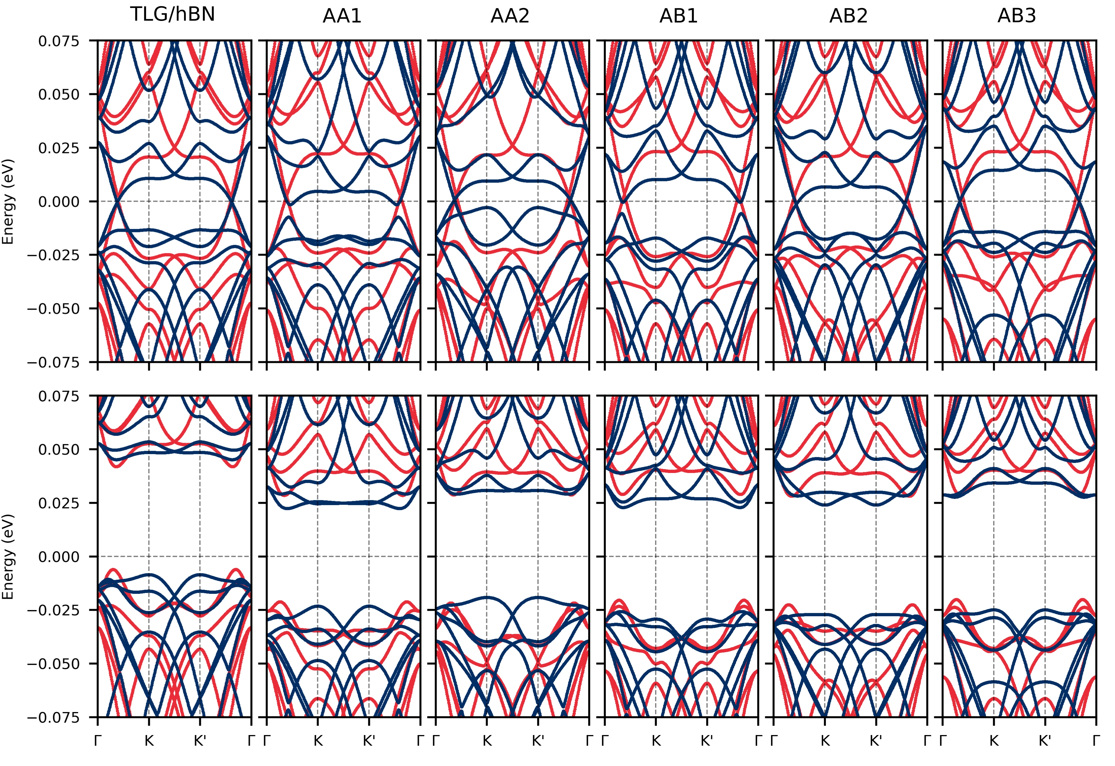
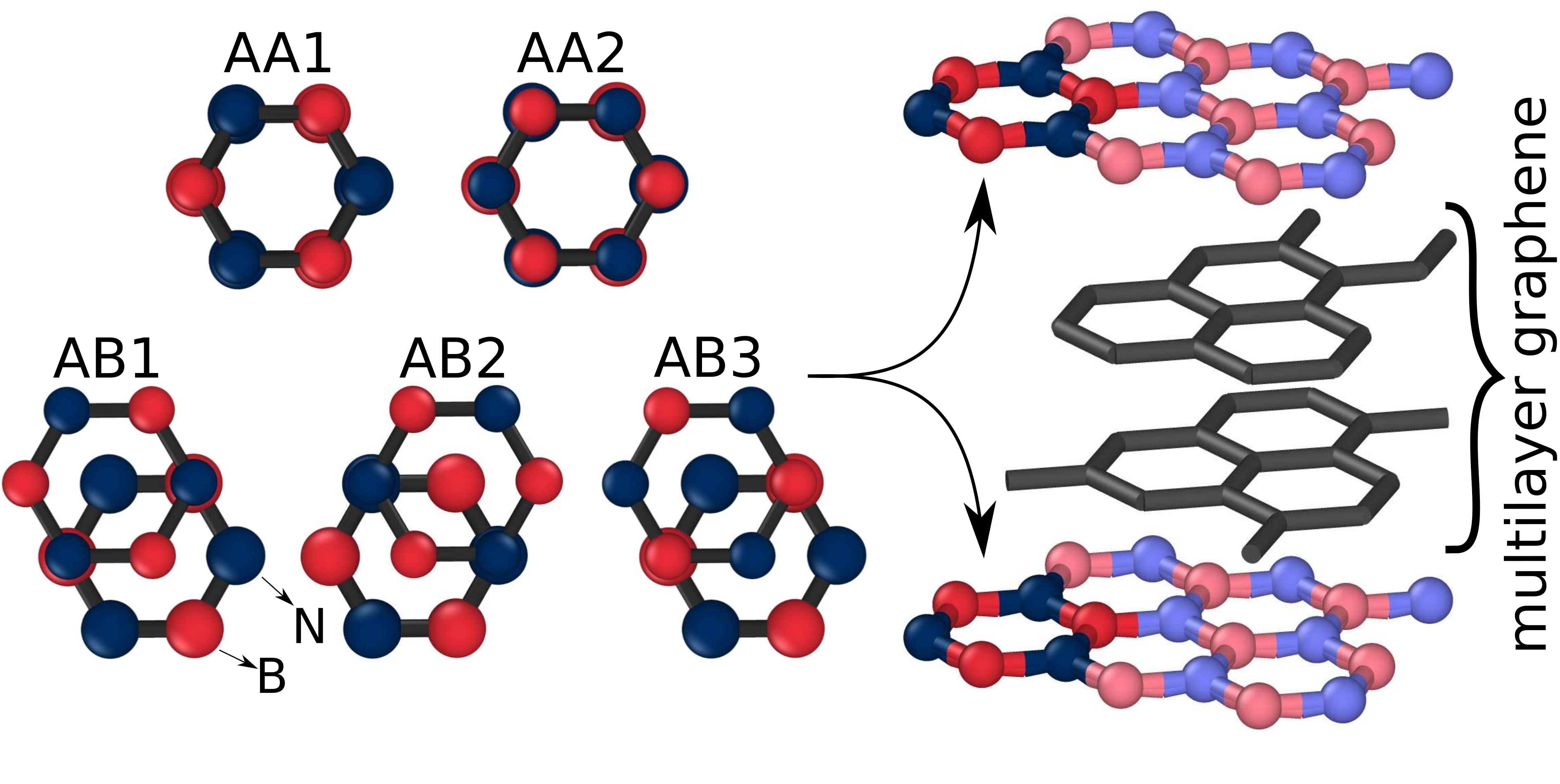
Recent studies [16, 32] have shown that ABC-stacked TLG on hBN is a suitable platform for the formation of gate-tunable flatbands. While the ABA (Bernal) stacking is the preferred low energy configuration and most commonly occurring stacking for trilayer graphene, it is not consider in this work. In this case, the low energy bandstructure consists of a combination of linear and quadratic bands. In the presence of a perpendicular electric field, the overlap between these bands can be tuned but this does not a give rise to an electrically tuned gap at the PDP as it does in the ABC stacking configuration. ABC stacked trilayer graphene, while less abundant, is still readily obtainable and frequently used in experiments. In light of this, we perform real-space tight-binding calculations for the whole moiré supercell of the encapsulated ABC trilayer graphene in which now the hBN layers are added in an atomistic way. We further include relaxation effects by performing semi-classical molecular dynamics simulations. The absence of gaps in our simplified model (3) and the lack of inclusion of the pseudo-vector potential term, indicates the importance of the PMF in the formation of gaps. Relaxation effects on the other hand are known to induce a large PMF due to intralayer hopping modulation [29, 12, 27], thus becoming a crucial ingredient in this calculation. In what follows, we select five highly symmetric stacking configurations of the hBN layers as shown in figure 1, to preserve the highest degree of symmetry, and which are all aligned as we are interested only in band reconstruction at a singular energy level.
The resulting electronic band-structures for the encapsulated ABC-stacked TLG configurations are shown in figure 2. The Dirac cone is now positioned between the original K-point and the -point due to a Lifshitz transition near the Dirac point coming from the hopping between the top and the bottom graphene layer, and is a typical feature seen in ABC TLG [31]. No effective spectral gap is observed for the unrelaxed systems besides the band anti-crossing near the -point in some cases and a tiny gap at the PDP when inversion symmetry is broken. The emergence of the band anti-crossing is presumably due to the PMF-term in equation 1 as no such gap was observed in our analysis based on the simplified model, shown in the supplementary material section 1. It is only after relaxation effects are taken into consideration that gaps emerge at the SDP. This supports our preceding intuition that the gaps are enhanced by the PMF, as relaxation induces a large PMF in each graphene layer. Previous work has shown the presence of a gate-tunable isolated flat band in TLG on monolayer hBN (TLG/hBN) and the emergence of highly correlated states both in experiment and theory [16, 32]. The band in question is the first valence band, which in our model reaches bandwidth of 17 meV (38 meV) for the relaxed (unrelaxed) case, for the same gating value that induces a potential difference of 10 meV between the top and the bottom graphene layer. There is however some slight overlap of the valence band with lower-lying bands, i.e. it is not fully isolated. For the other stacking configurations with relaxation included we observed similar flattening of the conduction band, the smallest bandwidth being 11 meV for AA1 stacking at 100 mV/nm, 11 meV for AB3 at 150 mV/nm, and 5 meV for TLG/hBN at 150 mV/nm gating field. We note that the magnitude of the gaps is dependent on the strength of the coupling to the hBN layers. In section 2 of the supplementary material we show results with a different parameter set for the coupling between graphene and hBN. We find that the gaps at the PDP and SPD are smaller and the bandwidth is larger when the coupling is weaker. In order to have a precise quantitative prediction of the induced gaps, tight-binding parameters based on accurate ab-initio simulations of the graphene/hBN interface are needed.
II.3 AB-stacked bilayer graphene
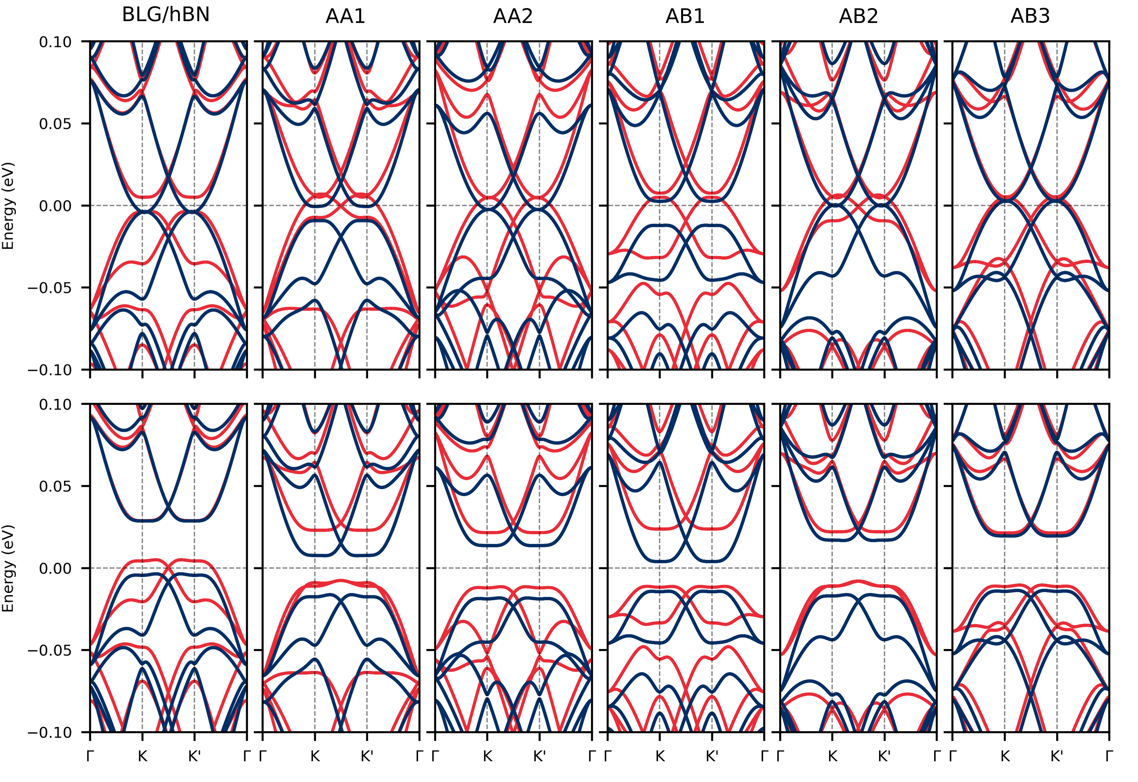
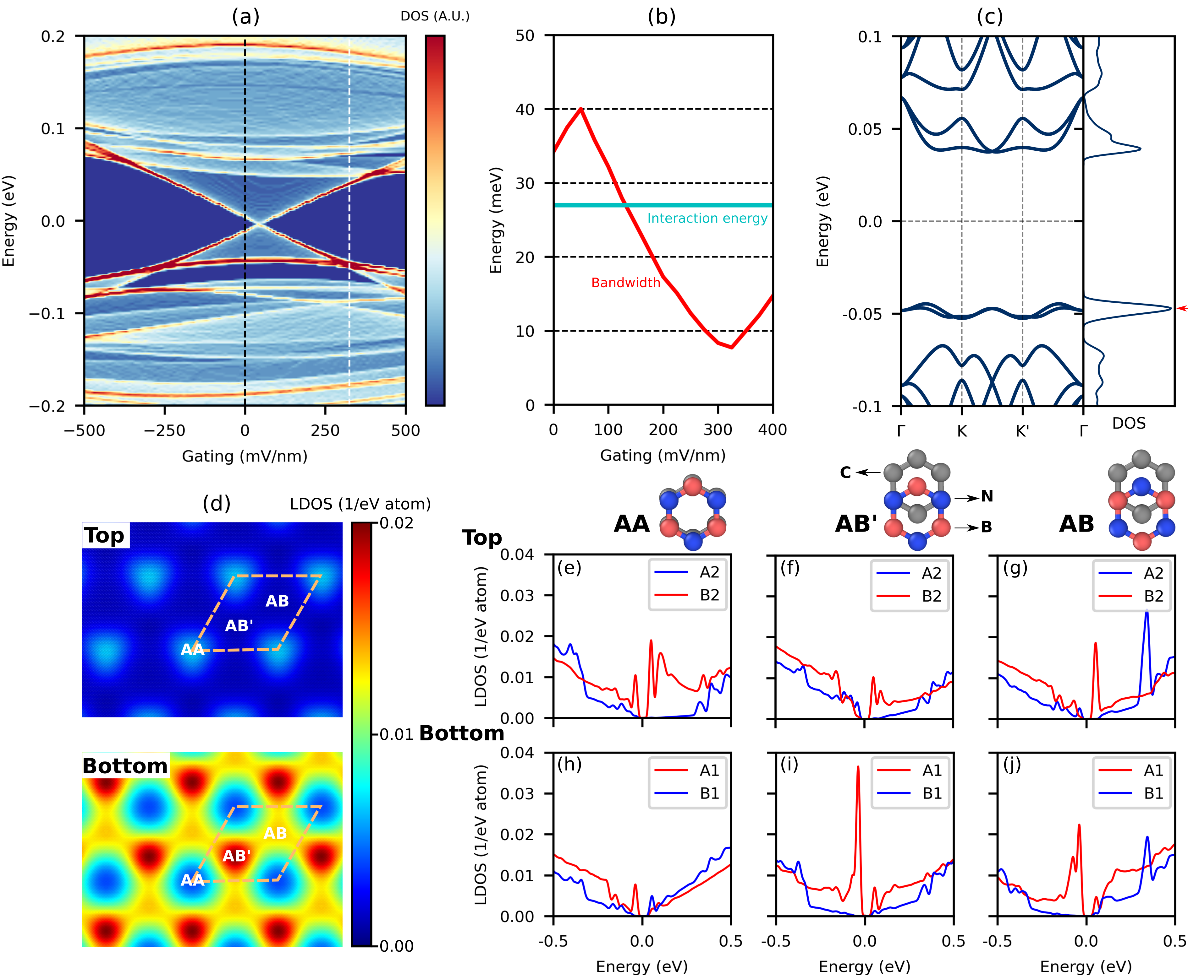
We next perform similar atomistic tight-binding calculations for the hBN-encapsulated configurations of AB-stacked bilayer graphene. The resulting band-structures are shown in figure 3. For one configuration, the AB1 stacking of hBN, a large effective gap appears at the SDP that is robust under relaxation. For this configuration the effective scalar moiré potentials on top and bottom graphene layer are identical, with opposite sign for the intralayer mass terms and , which maximizes the amplitude of the moiré term in the 2-component model for BLG and leading to strongly reduced Fermi-velocity at the SDP. The gap also remains unchanged when gating is applied and the gap at the PDP increases, which is apparent from figure 4(a) where the DOS is zero at a nearly constant energy between gating values of 350 mV/nm. A similar gap is seen for AB2, but closes after relaxation is included. In general we also find that a small gap at the PDP appears whenever the inversion symmetry is broken, which is the case for BLG/hBN, AA1 and AB1 configurations. After the structures are relaxed, these gaps get enhanced even further, except for BLG/hBN in which the gap becomes vanishingly small, which is in agreement with experimental observations [33]. For these systems the application of a perpendicular gate potential will first close the gap at the PDP as it counteracts the average non-zero mass term, after which the gap is opened up again - as seen in figure 4(a). The broken inversion symmetry and gap at the PDP in the BLG/hBN, AA1 and AB1 configurations leads to layer polarization which could further indicate the presence of unconventional ferroelectricity as was recently observed experimentally [34] and described theoretically [35] in twisted hBN/BLG/hBN systems. For completeness, in section 4 of the supplementary material, we provide the DOS of each configuration for each sublattice, showing the layer polarization in BLG/hBN, AA1 and AB1.
We next turn the attention to the gap at the SDP in the AB1 BLG configuration, that will squeeze the first valence band in width in the presence of gating. As plotted in figure 4(b), the bandwidth decreases down to 7 meV for an applied gating field of 325 mV/nm, which corresponds to a potential difference of 325 mV across the thickness of the sample (1 nm). Such electric field values across a thin 2D heterostructure lay well within reach of experimental capabilities. Most recently, Refs. 36 and 37 reported realizations of an electric field up to 3.5 V/nm across a bilayer using ionic liquid gates, one order of magnitude higher than required in this work. In figure 4(c) the band structure for the relaxed AB1 BLG configuration is presented with an applied electric field of 325 mV/nm, clearly showing the well-isolated first valence band and its ultra-flat dispersion. The effective gap to the second valence band is about 15 meV. The narrow bandwidth comes with a strong localization of the electronic wavefunction. The local density of states (LDOS) at -0.05 eV for the relaxed AB1 system with gating of 325 mV/nm is shown in figure 4(d), together with the LDOS for the energy range of -0.5 eV to 0.5 eV at the different local stacking arrangements in the top and bottom layer in panels (e)-(j) of the same figure. The wavefunction is strongly localized at the low-energy sites in the AB’ regions in the bottom layer. This is due to the gating, which induces a negative potential on the bottom and positive potential on the top layer. The Coulomb interaction energy can be estimated by taking the distance between charge carriers as the distance between the AB’ regions, which is nothing more than the periodic length nm of the moiré pattern. We find then that meV, where is the dielectric constant of hBN and the inter-particle distance. In figure 4(c) we compare this energy to the bandwidth, serving as an estimate for the kinetic energy of the charge carriers. One sees that upon gating , so that we enter a regime where the interaction energy dominates, which is expected to lead to highly-correlated electron-electron states in the first valence band. This is similar to magic-angle twisted bilayer graphene, where the localization is in the AA stacked regions with a moiré length of 13 nm, as well as TLG/hBN where the moiré length is identical.
II.4 Structural relaxation
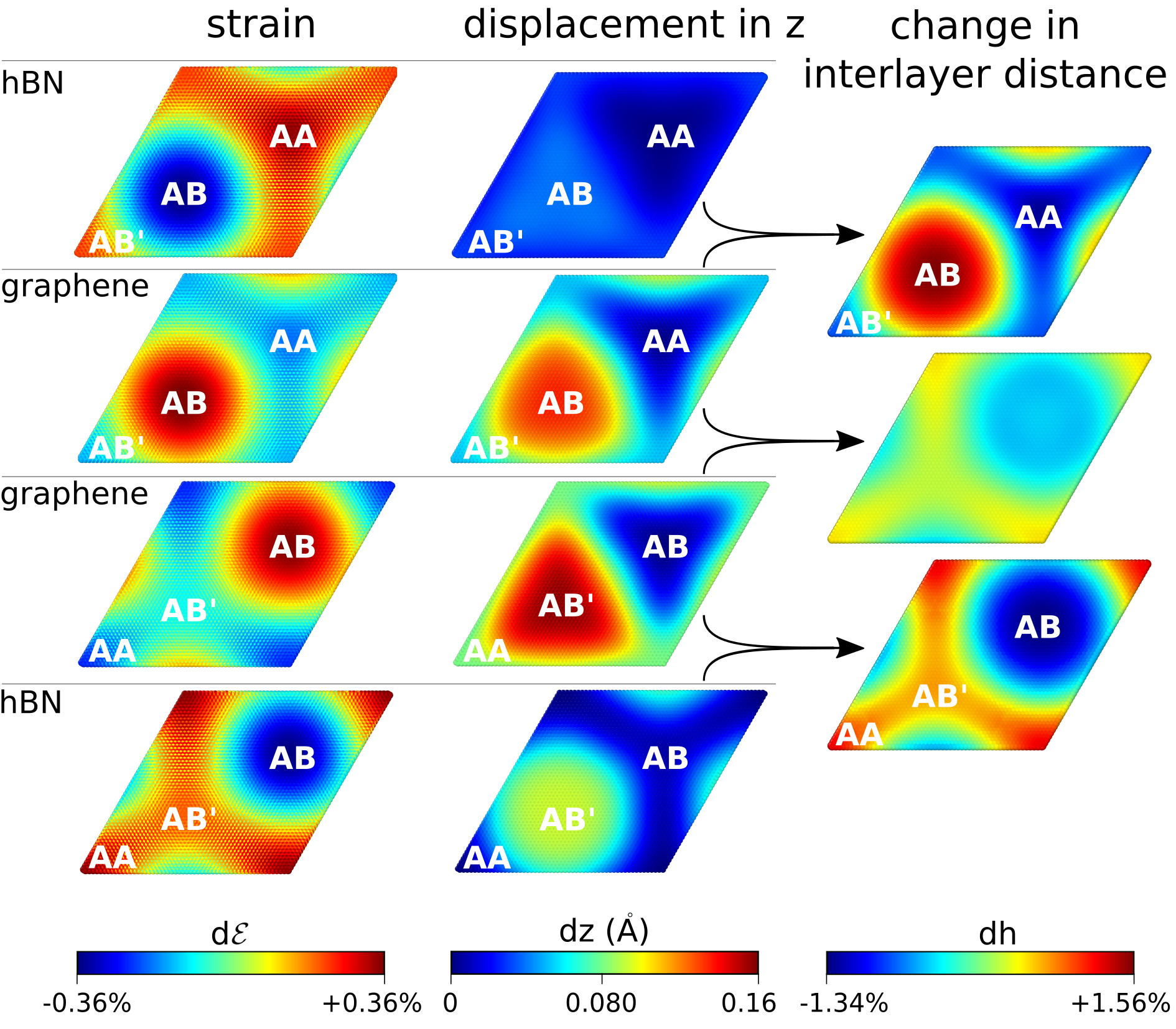
To better understand the effects of structural relaxation on the electronic properties we provide a qualitative analysis of the modifications due to the relaxation of the AA1-encapsulated bilayer graphene, plotted in figure 5. It is important to note that in order to couple the system to a flat substrate as is often the case in electronic devices and in order to suppress out-of-plane buckling, the top hBN layer is coupled to a 1D 12/6-Lennard-Jones potential , with parameters and . The relaxation strain forms a trigonal pattern, where in the regions with AB stacking, the graphene layers will stretch the most while the hBN layers will compress the most, decreasing the lattice mismatch and effectively increasing the AB region in size. Within the surrounding AA and AB’ stacking regions the opposite emerges, where now the graphene layers compress and the hBN layers expand, the compression (expansion) is the largest in the AA region within the graphene (hBN) layers and extends along lines connecting AA and AB’ regions. This again means that within the AA- and to a lesser extent AB’-regions the lattice mismatch is increased and the AA- and AB’- regions decrease in size. The AB stacking is the most energetically favorable while the AA stacking is the least favorable one, so that the expansion and compression of the AB and AA regions respectively minimizes the energy [38, 39, 29]. The strain within the graphene layer is in good agreement with Ref. 38 while the strain within the hBN layers here ranges from -0.39% to +0.36%, which is larger than in Ref. 38 where it ranges from -0.15% to +0.20%. This discrepancy can be largely attributed to the suppression of out-of-plane buckling due to the Lennard-Jones interaction with the top hBN layer. The strain of adjacent layers also seems to have little-to-no influence on the strain in other layers in the structure. In the supplementary material section 6 we show that the resulting modulation of the hoppings gives rise to a PMF on the order of 9 T. The out-of-plane displacement of individual layers in this case reaches values of up to 0.082 Å, with the effect being much stronger in the graphene layers than in the hBN layers. Moreover, the displacement seems to be always localized in the same place for each layer. In our case the buckling is determined by the stacking of the bottom graphene and hBN layers, as the bottom hBN layer does not contain a Lennard-Jones potential. In the bottom graphene and hBN layer, the AB-stacked regions buckle with the concave side in the graphene layer and the AB’-stacking region with the concave side in the hBN layer, also in agreement with Ref. [38]. The hBN-graphene interlayer distance varies on the order of of the original interlayer distance, which modulates the hoppings by approximately 0.03 or 0.01 eV, making it a rather weak effect. Especially the observed variation in interlayer distance between the graphene layers is insignificantly small.
III Conclusion
In conclusion, the hBN-encapsulated AB-stacked bilayer graphene was shown to be an ideal platform for the generation of low-dispersive bands and strong localization of electronic states, where stacking of hBN layers in combination with gating leads to a new mechanism for flattening the bands and tailoring the strongly-correlated states. By individually tuning the gap at the primary and the secondary Dirac point (by gating and by stacking of hBN layers, respectively), we were able to generate flat bands with a bandwidth below 10 meV, significantly lower than the estimated Coulomb interaction energy - hence facilitating the emergence of highly-correlated electron states. The achieved bandwidth is similar to that of twisted BLG [13, 14] ( 5-10 meV) and TLG/hBN [32, 16] ( 11.7 meV) where strongly-correlated phases have readily been observed and where the localization of charge carriers was on a similar length scale as was found here (so that the on-site Coulomb energy is similar as well). Encapsulating graphene with hBN layers is readily used to drastically improve the electronic properties of graphene, but our findings reveal that stacking of hBN layers is a relevant and potent ingredient to achieve high quality devices with gate-tunable strongly-correlated electronic states.
IV Methods
IV.1 Tight-binding model
The system is described by a tight-binding model, where a Bloch wavefunction of the form
| (4) |
is used with wavefunction of atomic site i at position . The most general form of the Hamiltonian is then given by
| (5) |
The first term in equation (5) defines the hopping between any sites i and j with a hopping strength t. The second term represents the potential due to the on-site potentials ( for carbon, eV for boron and eV for nitrogen). The matrix representation in the basis of the wavefunctions is then .
We make use of the Slater-Koster (SK) type of functions [40], which, depending on the type of orbitals and their relative positions, give a good estimate of the hopping value. In this work we closely follow the approach and parameters as described in Ref. 10 , leading to
| (6) |
where
| (7) | |||
| (8) |
Here = 0.026 nm is the decay length, = 0.142 nm the interatomic distance in graphene, = 0.335 nm the interlayer distance between graphene layers, = 0.48 eV, and = -2.7 eV. The exponential decay is set up in such a way that nnn hopping equals 0.1, given that in most literature for graphene. This specific adjustment was respected to further determine all the hoppings within the bilayer graphene systems for both unrelaxed and relaxed systems.
For ABC TLG another set of parameters was used due to the presence of next-nearest layer hoppings. From Ref. 41 we obtained = -2.577 eV, = 0.348 eV, = -0.024 eV, = 0.290 eV, = 0.196 eV and = -0.258 eV. For the hopping between neighbouring graphene and hBN layers, we rely again on the use of the SK functions to estimate the hopping parameters and adjust and in (7) and (8) accordingly. For the graphene in the relaxed systems we then use:
| (9) |
where is the hopping as calculated in equation (6), and is the atomic separation for the unrelaxed system.
A symmetric top-back gating is applied by introducing a potential field along the direction , where in all the atomic sites within the same layer the same potential was applied.
In order to set up and solve the tight-binding model we made use of Pybinding [42], which uses an efficient routine to setup and solve the band-structure, and relies on the KPM method [43] in order to obtain the electronic DOS. In this work a Gaussian broadening of 5 meV width was used in the KPM formalism (unless mentioned otherwise). A cutoff range for hopping-pairs to form was set to 1.75 times the graphene inter-atomic distance for intralayer hoppings, and 1.40 times the interlayer distance between graphene layers for interlayer hoppings. Next-nearest neighbours (nnn) in the graphene layers were included to improve the accuracy of our calculations and possibly capture any effects, such as electron-hole asymmetry, that might occur. It is known that the inclusion of nnn results in an energy shift of the Dirac point equivalent to three times the next-nearest-neighbor hopping , therefore a shift in energy of the same amount was applied such that the Dirac point sits at the Fermi level, which is 0.774 eV for TLG and 0.81 eV for BLG.
IV.2 Relaxation
The relaxation was performed through a classical molecular dynamics simulation as implemented in LAMMPS [44, 45], for all the layers simultaneously. For intra- and interlayer carbon-carbon interactions we used the bond-order Brenner potentials [46] and Kolmogorov-Crespi potentials [47] respectively. For the boron-nitrogen intralayer interactions we used Tersoff potentials [48], and the Morse potential for the interaction between graphene and hBN layers [38]. For the Morse potential we used as equilibrium distances 3.54 Å for B-C and 3.52 Å for N-C. In order to mimic the effects of a substrate, a 12/6-Lennard-Jones potential , with parameters and , is used to couple the system to a flat surface. This suppresses the out-of-plane buckling that otherwise commonly occurs in these systems. A single moiré supercell with periodic boundary conditions is then simulated at zero temperature starting from the unrelaxed configuration. The total energy of the system is minimized until the forces reach a value below eV/Å.
Conflicts of interest
There are no conflicts to declare.
Acknowledgements.
The authors would like to acknowledge the contribution of Miša Andelković, providing invaluable support leading up to this work. The work was supported by the Research Foundation - Flanders (FWO-Vl), project number G0A5921N. The computational resources were provided by the HPC core facility CalcUA of the Universiteit Antwerpen, and VSC (Flemish Supercomputer Center).References
- Bolotin et al. [2008] K. Bolotin, K. Sikes, Z. Jiang, M. Klima, G. Fudenberg, J. Hone, P. Kim, and H. Stormer, Ultrahigh electron mobility in suspended graphene, Solid State Commun. 146, 351 (2008).
- Decker et al. [2011] R. Decker, Y. Wang, V. W. Brar, W. Regan, H.-Z. Tsai, Q. Wu, W. Gannett, A. Zettl, and M. F. Crommie, Local electronic properties of graphene on a BN substrate via scanning tunneling microscopy, Nano Lett. 11, 2291 (2011).
- Dean et al. [2010] C. R. Dean, A. F. Young, I. Meric, C. Lee, L. Wang, S. Sorgenfrei, K. Watanabe, T. Taniguchi, P. Kim, K. L. Shepard, and J. Hone, Boron nitride substrates for high-quality graphene electronics, Nat. Nanotech. 5, 722 (2010).
- Xue et al. [2011] J. Xue, J. Sanchez-Yamagishi, D. Bulmash, P. Jacquod, A. Deshpande, K. Watanabe, T. Taniguchi, P. Jarillo-Herrero, and B. J. LeRoy, Scanning tunnelling microscopy and spectroscopy of ultra-flat graphene on hexagonal boron nitride, Nat. Mater. 10, 282 (2011).
- Chen et al. [2008] J.-H. Chen, C. Jang, S. Xiao, M. Ishigami, and M. S. Fuhrer, Intrinsic and extrinsic performance limits of graphene devices on SiO2, Nat. Nanotech. 3, 206 (2008).
- Park et al. [2008] C.-H. Park, L. Yang, Y.-W. Son, M. L. Cohen, and S. G. Louie, New generation of massless dirac fermions in graphene under external periodic potentials, Phys. Rev. Lett. 101, 126804 (2008).
- Yankowitz et al. [2012] M. Yankowitz, J. Xue, D. Cormode, J. D. Sanchez-Yamagishi, K. Watanabe, T. Taniguchi, P. Jarillo-Herrero, P. Jacquod, and B. J. LeRoy, Emergence of superlattice dirac points in graphene on hexagonal boron nitride, Nat. Phys. 8, 382 (2012).
- Wallbank et al. [2013] J. R. Wallbank, A. A. Patel, M. Mucha-Kruczynski, A. K. Geim, and V. I. Fal’ko, Generic miniband structure of graphene on a hexagonal substrate, Phys. Rev. B 87, 245408 (2013).
- Wallbank et al. [2015] J. R. Wallbank, M. Mucha-Kruczyński, X. Chen, and V. I. Fal’ko, Moiré superlattice effects in graphene/boron-nitride van der waals heterostructures: Moiré superlattice effects in graphene/boron-nitride van der waals heterostructures, Ann. Phys. (Berlin) 527, 359 (2015).
- Moon and Koshino [2014] P. Moon and M. Koshino, Electronic properties of graphene hexagonal boron nitride moiré superlattice, Phys. Rev. B 90, 155406 (2014).
- Cea et al. [2020] T. Cea, P. A. Pantaleón, and F. Guinea, Band structure of twisted bilayer graphene on hexagonal boron nitride, Phys. Rev. B 102, 155136 (2020).
- Jung et al. [2017] J. Jung, E. Laksono, A. M. DaSilva, A. H. MacDonald, M. Mucha-Kruczyński, and S. Adam, Moiré band model and band gaps of graphene on hexagonal boron nitride, Phys. Rev. B 96, 085442 (2017).
- Cao et al. [2018a] Y. Cao, V. Fatemi, S. Fang, K. Watanabe, T. Taniguchi, E. Kaxiras, and P. Jarillo-Herrero, Unconventional superconductivity in magic-angle graphene superlattices, Nature 556, 43 (2018a).
- Cao et al. [2018b] Y. Cao, V. Fatemi, A. Demir, S. Fang, S. L. Tomarken, J. Y. Luo, J. D. Sanchez-Yamagishi, K. Watanabe, T. Taniguchi, E. Kaxiras, R. C. Ashoori, and P. Jarillo-Herrero, Correlated insulator behaviour at half-filling in magic-angle graphene superlattices, Nature 556, 80 (2018b).
- Chittari et al. [2019] B. L. Chittari, G. Chen, Y. Zhang, F. Wang, and J. Jung, Gate-tunable topological flat bands in trilayer graphene boron-nitride moiré superlattices, Phys. Rev. Lett. 122, 016401 (2019).
- Chen et al. [2019a] G. Chen, L. Jiang, S. Wu, B. Lyu, H. Li, B. L. Chittari, K. Watanabe, T. Taniguchi, Z. Shi, J. Jung, Y. Zhang, and F. Wang, Evidence of a gate-tunable mott insulator in a trilayer graphene moiré superlattice, Nat. Phys. 15, 237 (2019a).
- Zhang et al. [2021] X. Zhang, K.-T. Tsai, Z. Zhu, W. Ren, Y. Luo, S. Carr, M. Luskin, E. Kaxiras, and K. Wang, Correlated Insulating States and Transport Signature of Superconductivity in Twisted Trilayer Graphene Superlattices, Physical Review Letters 127, 166802 (2021), publisher: American Physical Society.
- Suárez Morell et al. [2010] E. Suárez Morell, J. D. Correa, P. Vargas, M. Pacheco, and Z. Barticevic, Flat bands in slightly twisted bilayer graphene: Tight-binding calculations, Physical Review B 82, 121407 (2010).
- Zhu et al. [2020] Z. Zhu, S. Carr, D. Massatt, M. Luskin, and E. Kaxiras, Twisted trilayer graphene: A precisely tunable platform for correlated electrons, Phys. Rev. Lett. 125, 116404 (2020).
- Wu et al. [2021] Z. Wu, Z. Zhan, and S. Yuan, Lattice relaxation, mirror symmetry and magnetic field effects on ultraflat bands in twisted trilayer graphene, Sci. China Phys. Mech. Astron. 64, 267811 (2021).
- Marchenko et al. [2018] D. Marchenko, D. V. Evtushinsky, E. Golias, A. Varykhalov, T. Seyller, and O. Rader, Extremely flat band in bilayer graphene, Sci. Adv. 4, eaau0059 (2018).
- Mayorov et al. [2011] A. S. Mayorov, R. V. Gorbachev, S. V. Morozov, L. Britnell, R. Jalil, L. A. Ponomarenko, P. Blake, K. S. Novoselov, K. Watanabe, T. Taniguchi, and A. K. Geim, Micrometer-scale ballistic transport in encapsulated graphene at room temperature, Nano Lett. 11, 2396 (2011).
- Kretinin et al. [2014] A. Kretinin, Y. Cao, J.-S. Tu, G. Yu, R. Jalil, K. Novoselov, S. Haigh, A. Gholinia, A. Mishchenko, M. Lozada, T. Georgiou, C. Woods, F. Withers, P. Blake, G. Eda, A. Wirsig, C. Hucho, K. Watanabe, T. Taniguchi, and R. Gorbachev, Electronic properties of graphene encapsulated with different two-dimensional atomic crystals, Nano Lett. 14, 3270 (2014).
- Oka and Koshino [2021] H. Oka and M. Koshino, Fractal energy gaps and topological invariants in hBN/graphene/hBN double moiré systems, Phys. Rev. B 104, 035306 (2021).
- Andelković et al. [2020] M. Andelković, S. P. Milovanović, L. Covaci, and F. M. Peeters, Double moiré with a twist: supermoiré in encapsulated graphene, Nano Lett. 20, 979 (2020).
- Wang et al. [2019] L. Wang, S. Zihlmann, M.-H. Liu, P. Makk, K. Watanabe, T. Taniguchi, A. Baumgartner, and C. Schönenberger, New generation of moiré superlattices in doubly aligned hBN/graphene/hBN heterostructures, Nano Lett. 19, 2371 (2019).
- Long et al. [2021] M. Long, P. A. Pantaleón, Z. Zhan, F. Guinea, J. A. Silva-Guillén, and S. Yuan, An accurate description of the structural and electronic properties of twisted bilayer graphene-boron nitride heterostructures, npj Comput Mater 8, 73 (2021).
- Kuiri et al. [2021] M. Kuiri, S. K. Srivastav, S. Ray, K. Watanabe, T. Taniguchi, T. Das, and A. Das, Enhanced electron-phonon coupling in doubly aligned hexagonal boron nitride bilayer graphene heterostructure, Physical Review B 103, 115419 (2021).
- Jung et al. [2015] J. Jung, A. M. DaSilva, A. H. MacDonald, and S. Adam, Origin of band gaps in graphene on hexagonal boron nitride, Nat. Commun. 6, 6308 (2015).
- McCann and Koshino [2013] E. McCann and M. Koshino, The electronic properties of bilayer graphene, Rep. Prog. Phys. 76, 056503 (2013).
- Zhang et al. [2010] F. Zhang, B. Sahu, H. Min, and A. H. MacDonald, Band structure of A B C -stacked graphene trilayers, Phys. Rev. B 82, 035409 (2010).
- Chen et al. [2019b] G. Chen, A. L. Sharpe, P. Gallagher, I. T. Rosen, E. J. Fox, L. Jiang, B. Lyu, H. Li, K. Watanabe, T. Taniguchi, J. Jung, Z. Shi, D. Goldhaber-Gordon, Y. Zhang, and F. Wang, Signatures of tunable superconductivity in a trilayer graphene moiré superlattice, Nature 572, 215 (2019b).
- Kim et al. [2018] H. Kim, N. Leconte, B. L. Chittari, K. Watanabe, T. Taniguchi, A. H. MacDonald, J. Jung, and S. Jung, Accurate gap determination in monolayer and bilayer graphene/h-bn moiré superlattices, Nano Lett. 18, 7732 (2018).
- Zheng et al. [2020] Z. Zheng, Q. Ma, Z. Bi, S. de la Barrera, M.-H. Liu, N. Mao, Y. Zhang, N. Kiper, K. Watanabe, T. Taniguchi, J. Kong, W. A. Tisdale, R. Ashoori, N. Gedik, L. Fu, S.-Y. Xu, and P. Jarillo-Herrero, Unconventional ferroelectricity in moiré heterostructures, Nature 588, 71 (2020).
- Zhu et al. [2022] Z. Zhu, S. Carr, Q. Ma, and E. Kaxiras, Electric field tunable layer polarization in graphene/boron-nitride twisted quadrilayer superlattices, Physical Review B 106, 205134 (2022).
- Domaretskiy et al. [2022] D. Domaretskiy, M. Philippi, M. Gibertini, N. Ubrig, I. Gutiérrez-Lezama, and A. F. Morpurgo, Quenching the bandgap of two-dimensional semiconductors with a perpendicular electric field, Nat. Nanotech. , 1 (2022).
- Weintrub et al. [2022] B. I. Weintrub, Y.-L. Hsieh, J. N. Kirchhof, and K. I. Bolotin, Generating extreme electric fields in 2d materials by dual ionic gating, Nat. Commun. 13, 6601 (2022).
- Argentero et al. [2017] G. Argentero, A. Mittelberger, M. Reza Ahmadpour Monazam, Y. Cao, T. J. Pennycook, C. Mangler, C. Kramberger, J. Kotakoski, A. K. Geim, and J. C. Meyer, Unraveling the 3d atomic structure of a suspended graphene/hBN van der waals heterostructure, Nano Lett. 17, 1409 (2017).
- Woods et al. [2014] C. R. Woods, L. Britnell, A. Eckmann, R. S. Ma, J. C. Lu, H. M. Guo, X. Lin, G. L. Yu, Y. Cao, R. V. Gorbachev, A. V. Kretinin, J. Park, L. A. Ponomarenko, M. I. Katsnelson, Y. N. Gornostyrev, K. Watanabe, T. Taniguchi, C. Casiraghi, H.-J. Gao, A. K. Geim, and K. S. Novoselov, Commensurate–incommensurate transition in graphene on hexagonal boron nitride, Nat. Phys. 10, 451 (2014).
- Slater and Koster [1954] J. C. Slater and G. F. Koster, Simplified lcao method for the periodic potential problem, Phys. Rev. 94, 1498 (1954).
- Menezes et al. [2014] M. G. Menezes, R. B. Capaz, and S. G. Louie, Ab initio quasiparticle bandstructure of ABA and ABC-stacked graphene trilayers, Phys. Rev. B 89, 035431 (2014).
- [42] D. Moldovan, M. Andelković, and F. M. Peeters, Pybinding v0.9.5: A python package for tight-binding calculations, https://zenodo.org/record/4010216.
- Weiße et al. [2006] A. Weiße, G. Wellein, A. Alvermann, and H. Fehske, The kernel polynomial method, Rev. Mod. Phys. 78, 275 (2006).
- Plimpton [1995] S. Plimpton, Fast parallel algorithms for short-range molecular dynamics, Journal of Computational Physics 117, 1 (1995).
- Plimpton and Thompson [2012] S. J. Plimpton and A. P. Thompson, Computational aspects of many-body potentials, MRS Bull. 37, 513 (2012).
- Brenner et al. [2002] D. W. Brenner, O. A. Shenderova, J. A. Harrison, S. J. Stuart, B. Ni, and S. B. Sinnott, A second-generation reactive empirical bond order (REBO) potential energy expression for hydrocarbons, J. Phys.: Condens. Matter 14, 783 (2002).
- Kolmogorov and Crespi [2000] A. N. Kolmogorov and V. H. Crespi, Smoothest bearings: interlayer sliding in multiwalled carbon nanotubes, Phys. Rev. Lett. 85, 4727 (2000).
- Tersoff [1988] J. Tersoff, New empirical approach for the structure and energy of covalent systems, Phys. Rev. B 37, 6991 (1988).