Phase engineering in tantalum sulfide monolayers on Au(111)
Abstract
We prepare monolayers of tantalum sulfide on Au(111) by evaporation of Ta in a reactive background of H2S. Under sulfur-rich conditions, monolayers of 2H-TaS2 develop, whereas under sulfur-poor conditions TaS forms, a structure that can be derived from 2H-TaS2 by removal of the bottom S layer. We analyse the alignment of the layers with respect to the substrate and the relation with the domains in the Au(111) herringbone reconstruction using scanning tunneling microscopy (STM). With the help of density functional theory (DFT) calculations we can determine the registry of the two phases with the substrate. We develop a growth process that allows preparation of uniquely oriented 2H-TaS2 on Au(111). 2H-TaS2 and TaS have a remarkably similar in-plane lattice structure and we observe the formation of lateral 2H-TaS2-TaS heterostructures with atomically well-defined and defect-free boundaries. We observe mirror twin boundaries within 2H-TaS2 along the S- and Ta-edge.
1 Introduction
The properties of ultrathin materials are determined by composition, phase, and film thickness. Phase engineering is the rational use of the same ingredients to obtain different materials with varying properties, and potentially a powerful tool to tune unique functionalities and innovative properties of distinct systems according to the intended applications and, consequently, to enable their incorporation in future devices [1].
Ultrathin films with the same ingredients can have distinct properties depending on their stoichiometry and atomic coordination [2]. An especially rich field for phase engineering are materials (formally) derived from transition metal dichalcogenides (TMDCs) of the form MX2 (M = metal, X = chalcogen). Different phases can be favored depending on the growth conditions and modified through post-growth annealing processes [3]. Recently, there were several studies on chalcogen-poor variants of TMDCs, both in the form of self-intercalated layers [4] or monolayers with an ordered arrangement of chalcogen vacancies [5, 6].
The reduced symmetry is decisive for key properties of ultrathin TMDCs. Specifically, the loss of inversion symmetry when going from the bilayer to the monolayer in the 2H-phase [7] can directly lead to a spin-polarized electronic band structure. For example, in monolayer 2H-TaS2 the band crossing the Fermi level is spin-split in a large fraction of the Brillouin zone [8]. For fundamental reasons, the spin-splitting has to be reversed for points in the Brillouin zone linked by inversion symmetry, for example, the K and K’ point in a hexagonal crystal lattice, thereby enabling valleytronics [9].
Our study focuses on TMDCs composed of tantalum and sulfur. This system has a rich phase diagram in the bulk [10] which opens the door to the tuning of properties without changing the ingredients. A versatile method for the preparation of well-defined ultrathin layers of tantalum sulfide is epitaxial growth on single-crystalline substrates [8]. In our previous work [11] we discovered a sulfur-poor tantalum sulfide phase coexisting with the previously established monolayer 2H-TaS2. The 2H-phase is schematically shown in figures 1 (a) and (b). It has a honeycomb lattice where one sublattice is occupied by Ta and the other by two S on top of each other. Note that in the top view shown in figure 1 (a) the lower S is eclipsed by the upper one. The side view in figure 1 (b) shows the typical chalcogen-metal-chalcogen sandwich structure of TMDCs. The bonding between 2H-TaS2 and the substrate is mainly given by the van der Waals interaction [12]. The monolayer 2H-TaS2 phase was called -phase in Ref. [11], it will be simply referred to as TaS2 in this paper.
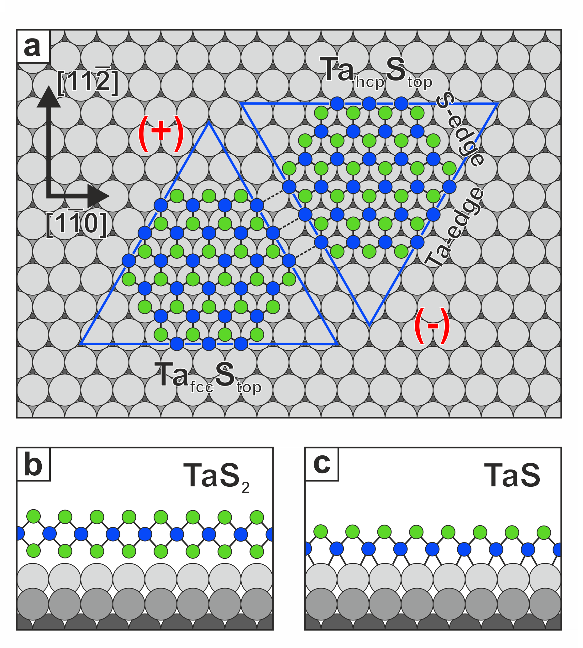
Under S-poor conditions a S-deficient phase can grow (-phase in Ref. [11]). We determined its stoichiometry as TaS2-x with . It will be called TaS in this paper to avoid cumbersome notation. When we refer to both phases at the same time we will use the neutral term tantalum sulfide. A slightly simplified model of TaS (for a full discussion see Ref. [11]) is shown in figure 1 (a) and (c). In the side view in figure 1 (c) the lower S layer is missing, the undercoordinated Ta atoms interact strongly with the Au substrate. Conveniently, we can use the same schematic top view (figure 1 (a)) as for TaS2 when we now interpret the green circle as a single S.
In this paper, we first describe the structure of both tantalum sulfide phases with special emphasis on the epitaxial relation with the substrate. We present a protocol for the preparation of TaS2/Au(111) with a unique orientation. Finally, we analyse boundaries between different phases and different orientations.
2 Methods
We used an ultra-high vacuum system (home-built, background pressure mbar). Samples were prepared in-situ, temperatures were measured by thermocouples in direct contact with the samples.
Au(111) was prepared by 1.5 keV Ar+ sputtering at room temperature followed by a high temperature sputter cycle at 900 K and annealing at 900 K. Cleanliness was verified by a well-defined low-energy electron diffraction (LEED) pattern and absence of impurities in scanning tunneling microscopy (STM).
Ta was evaporated from a mini e-beam evaporator (OAR EGCO4), the evaporation rate was calibrated by evaporation of Ta on Au(111) at room temperature followed by annealing at 500 K for 10 min leading to pseudomorphic Ta islands of monolayer height, the coverage of which is used to quantify the amount of Ta. H2S was dosed using a stainless steel tube (tube diameter cm, distance from tube opening to sample cm, angle between tube axis and sample normal ). The pressure was measured far away from the tube opening.
Tantalum sulfide was prepared by evaporation of Ta at a rate ML/min at room temperature up to a coverage of ML in an H2S atmosphere quantified by mbar, followed by an annealing step for min at K. During annealing and also until the sample temperature drops below 450 K is kept constant. Deviations from these standard parameters are given in the figure captions. A detailed study on the dependence of the distribution and morphology of the tantalum sulfides is given in our previous publication [11].
STM measurements were conducted at room temperature. Tunneling parameters (bias voltage , tunneling current ) are given for each image.
To perform spin-degenerate density functional theory (DFT) calculations we use the Vienna ab initio simulation package (projector augmented wave method) [13]. The generalized gradient approximation is applied to the exchange-correlation potential [14]. The Grimme semi-empirical method is used for the van der Waals correction [15]. We use the valence electron configurations Ta 5, 6, 6, S 3, 3, and Au 5, 6. An energy cut-off of 360 eV is employed for the plane-wave basis. For the supercell of 2H-TaS2 or TaS in contact with an Au(111) supercell (4 Au layers), a -mesh is used. Slab models are obtained by adding a vacuum layer of 15 Å thickness in the out-of-plane direction. The two Au layers farthest away from the interface are fixed at the atomic positions of bulk Au. The total energy convergence criterion of the self-consistency calculations is set to eV. The atomic positions and lattice constants are optimized until the Hellmann–Feynman forces remain below eV/Å and the remaining pressure is reduced to less than 1 kbar. STM images are simulated by the Tersoff–Hamann method [16]. Partial charges are calculated using Bader charge analysis [17].
3 Results and discussion
3.1 Structure, orientation, stacking, and registry
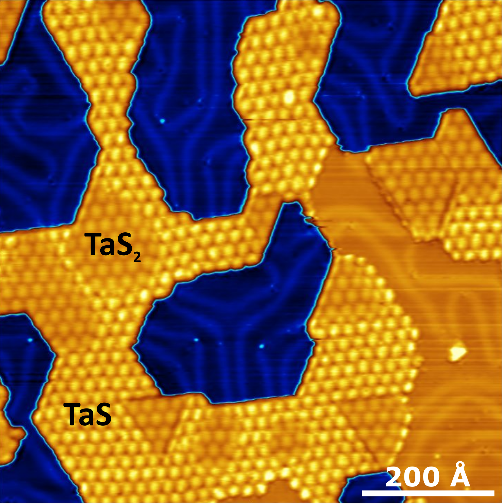
Figure 2 (a) shows an STM image of a sample where both TaS2 and TaS are present. We choose the color scale in a way that the gold substrate appears in shades of blue and TaS2 and TaS islands appear brown and yellow, respectively. Due to the lattice mismatch with the gold substrate both materials show a hexagonal moiré pattern. In this image, TaS2 and TaS islands are joint, forming a 2D heterostructure.
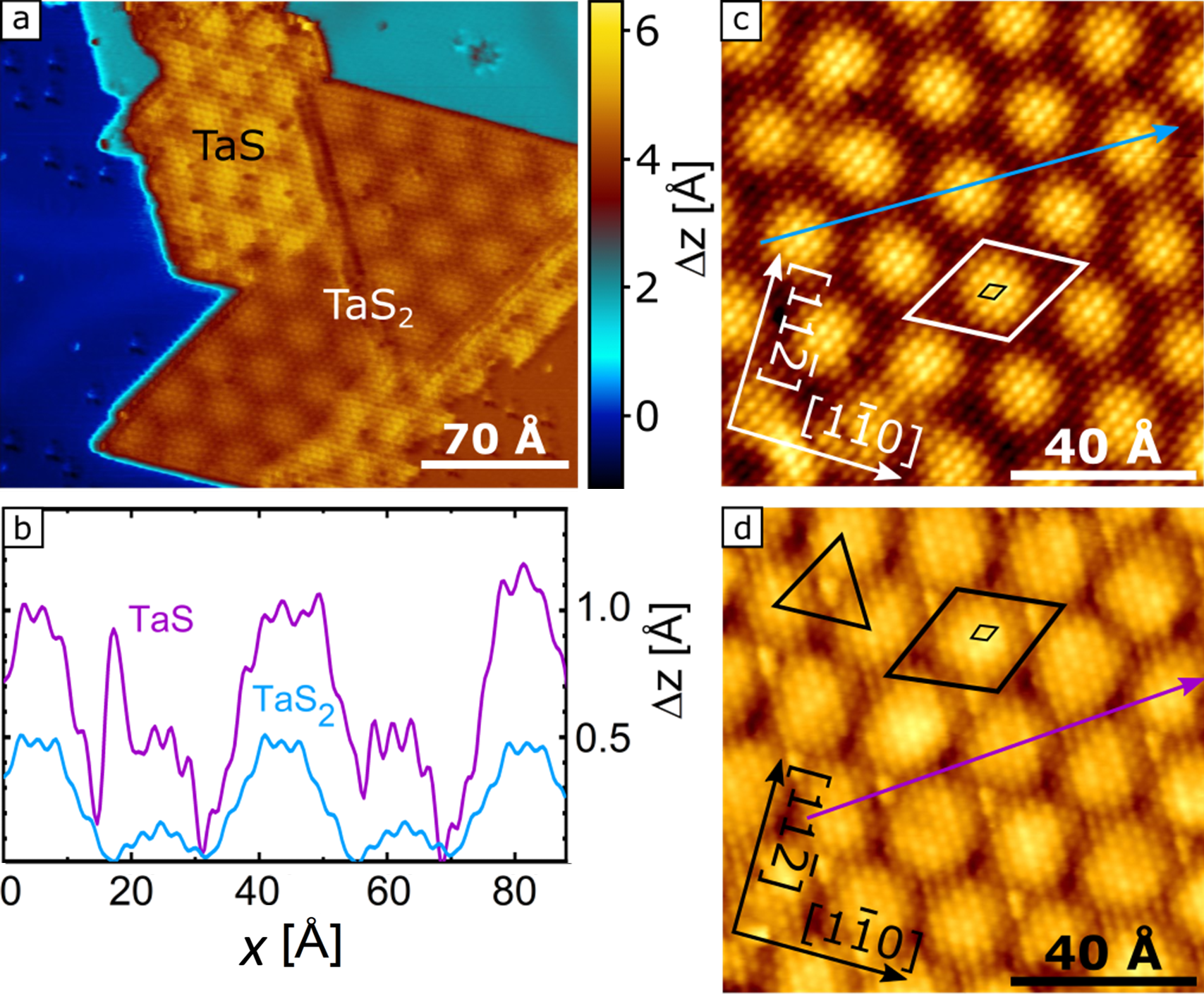
Figures 2 (c) and (d) show high-resolution STM images of TaS2 and TaS, respectively. Two periodicities are visible: the moiré periodicity and the much smaller periodicity of the atomic lattice. The unit cell of each lattice is indicated by large and small diamonds. Our previous work indicates that the bright protrusions of the atomic lattice are the S atoms [11].
The moiré structure arises from the variation of the registry between the Ta and S atoms on one hand and the Au substrate atoms on the other hand throughout the supercell, as discussed in detail in Ref. [12]. This is neglected in the schematic sketches shown in figure 1, where we depict the tantalum sulfides in a simplified superstructure. In this sketch, we select the local registry where the interaction between tantalum sulfide and Au(111) is strongest, which is found for the lower S on top of Au for the case of TaS2 and for Ta in a threefold-hollow site for the case of TaS. Note that handily this leads to the same schematic top view for both phases (figure 1 (a)). This specific registry is found in the regions that give rise to the bright maxima in the moiré cell [11].
TaS2 is very well ordered and uniform, exhibiting a smooth moiré modulation with a pronounced maximum in the center of the unit cell framed by two minima (figure 2 (c)). The moiré lattice is highly aligned with the TaS2 lattice, which proves that the dense-packed rows of TaS2 and Au(111) are aligned. A moiré analysis yields a lattice constant of Å [11]. The moiré pattern induces an average apparent corrugation of Å under the tunneling conditions used here (figure 2 (b)). The smooth variation and the low amplitude indicate a weak interaction with the substrate.
In contrast, the structure of TaS is more diverse and we can clearly distinguish three moiré areas (figure 2 (d)): a pronounced broad primary maximum in the center of the unit cell, a pronounced minimum (left part of the unit cell) and secondary bright area (right part of the unit cell), which often but not always exhibits one or more particularly bright spots. Also here the dense-packed rows of overlayer and substrate are aligned, the lattice constant is Å [11]. For the overall apparent corrugation we find Å (figure 2 (b)). The exact values of the moiré corrugation depend on the tunnel parameters, but TaS is always rougher than TaS2. Usually, the moiré corrugation of TaS is approximately twice as large as the moiré corrugation of TaS2. The more rough structure of TaS stems from a strong interaction with the Au surface.
Using DFT, we calculated the partial charges per tantalum sulfide unit cell of the individual layers (upper S, Ta, lower S, Au(111)) for both TaS2 and TaS, see table 1. For comparison, we include freestanding TaS2. TaS2 adsorbed on Au(111) is remarkably similar to freestanding TaS2. It is also noteworthy that with respect to charge transfer the upper S layer in TaS is almost identical to TaS2, which can explain the similar appearance in STM. Even though the partial charge of the Ta layer is different for the two sulfides, this difference is modest considering the fact that for TaS2 the Ta is covalently bound to six S, whereas for TaS it is only bound to three S and the substrate. The strongest difference is found for the partial charge of Au(111), which even changes sign.
| upper S | Ta | lower S | Au | |
|---|---|---|---|---|
| freestanding TaS2 | -0.82 | +1.93 | -0.82 | n.a. |
| TaS2/Au(111) | -0.83 | +1.60 | -0.84 | +0.07 |
| TaS/Au(111) | -0.86 | +1.44 | n.a. | -0.58 |
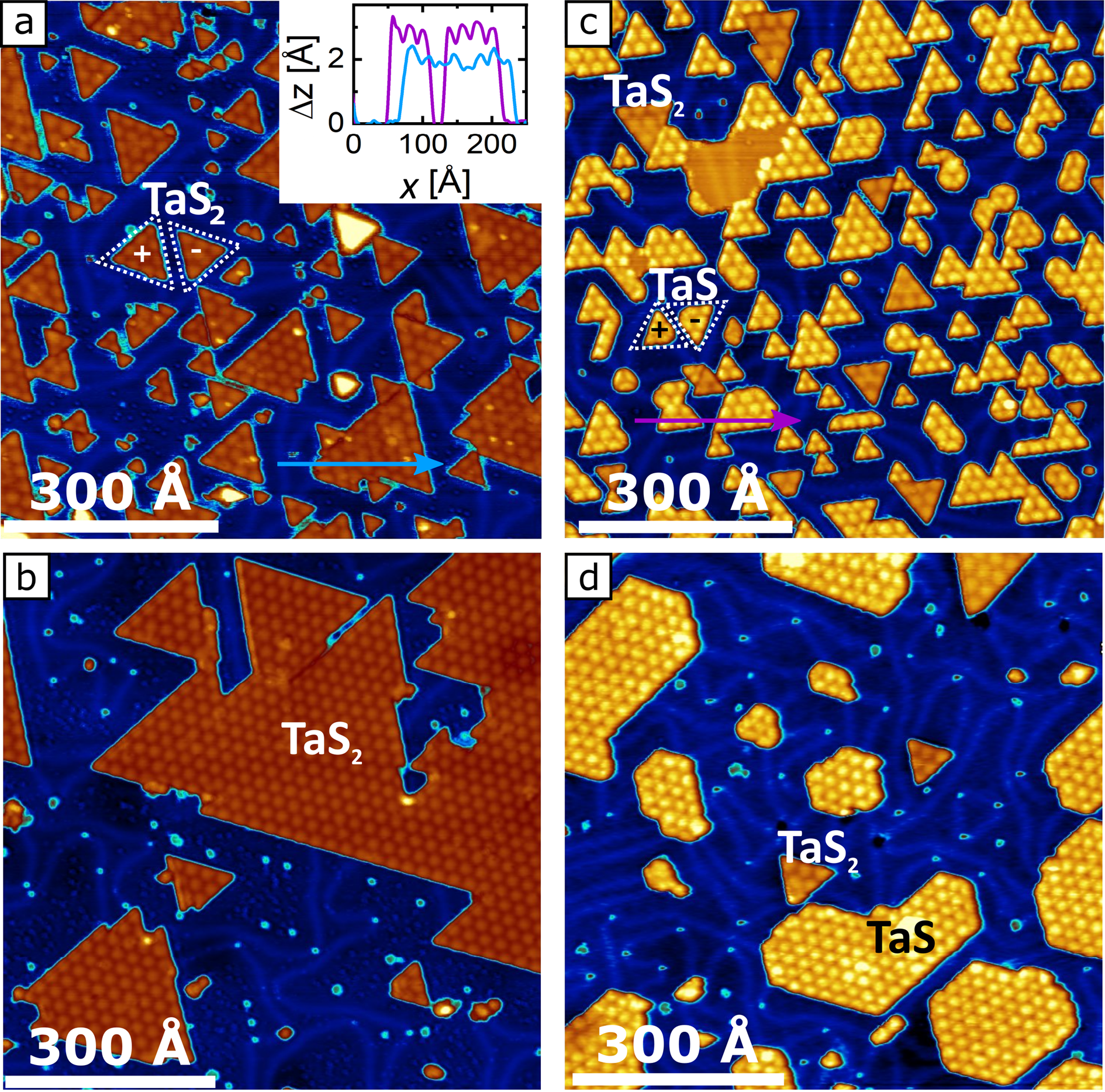
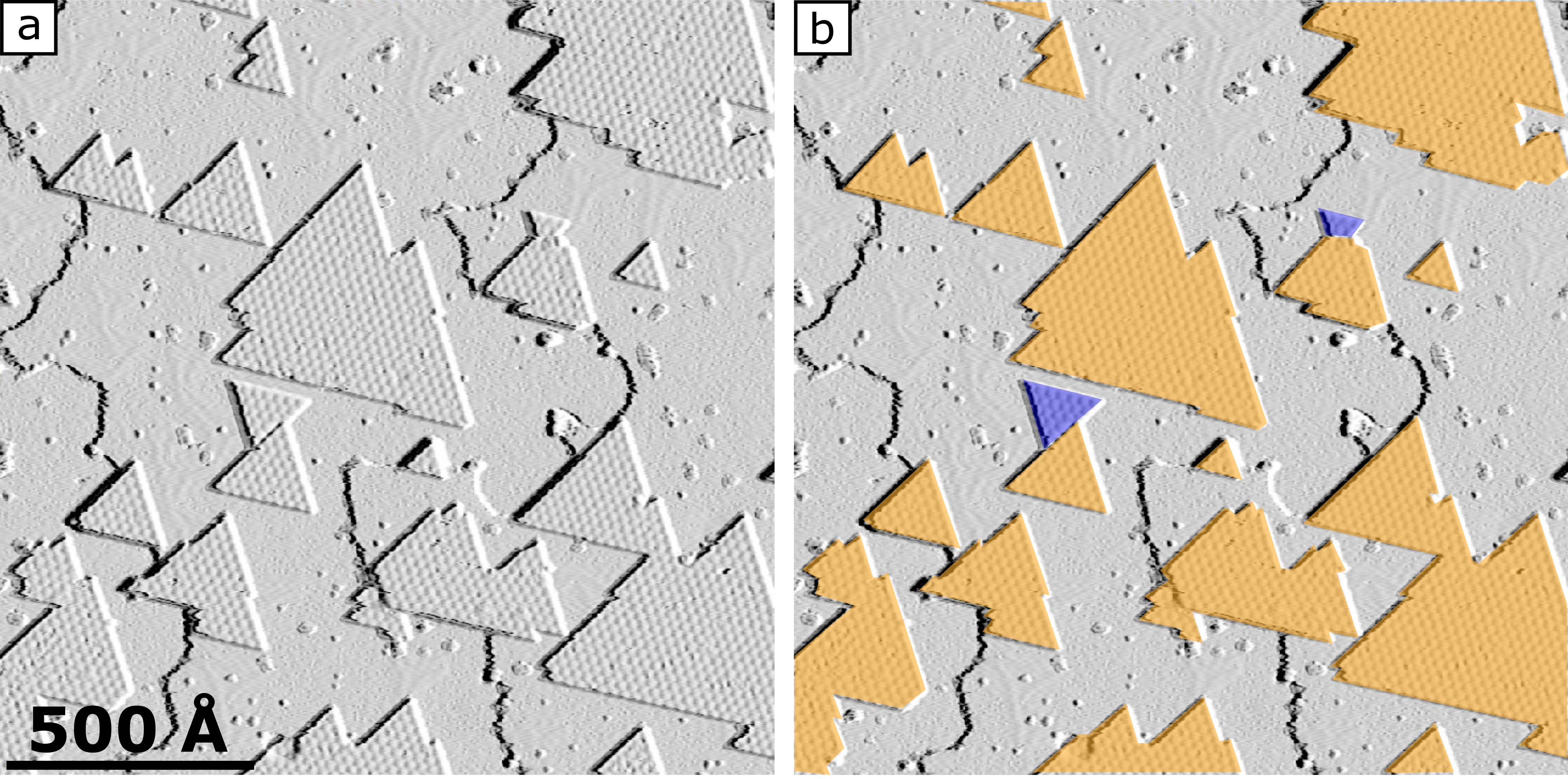
TaS2 islands on Au(111) prefer a triangular shape, as shown in figure 3 (a, b). The edges of the triangles are parallel to the dense packed atomic rows. We find two orientations that we denote (+) and (-), which differ by a rotation of . For (+), one tip of the triangular shaped island points along the -direction of the gold substrate, the other tips point along and . More formally: A vector from the midpoint between two vertices to the third vertex points along . For (-), the triangles point along (and , and ).
Also small TaS islands (figure 3 (c)) have a triangular shape, allowing us to use the classification (+)/(-) for this phase as well. Large TaS islands have a more hexagonal shape (figure 3 (d)).
For TaS there is another indicator of threefold symmetry: in figure 2 (d) we always find the secondary maximum in an up-pointing triangle formed by the primary maxima (marked in the figure). From small triangular TaS islands as those shown in figure 3 (c) we can deduce that this is a feature of the (+)-orientation, while for the (-)-orientation the situation is reversed. This allows us to determine the orientation also for hexagonally or irregularly shaped TaS islands as those in figure 3 (d).
We propose that the two different orientations that we determine phenomenologically from the alignment of triangular islands with respect to the substrate are due to two different orientations of the tantalum sulfide lattice linked by a -rotation as indicated in figure 1. This will be analysed in full detail further below.
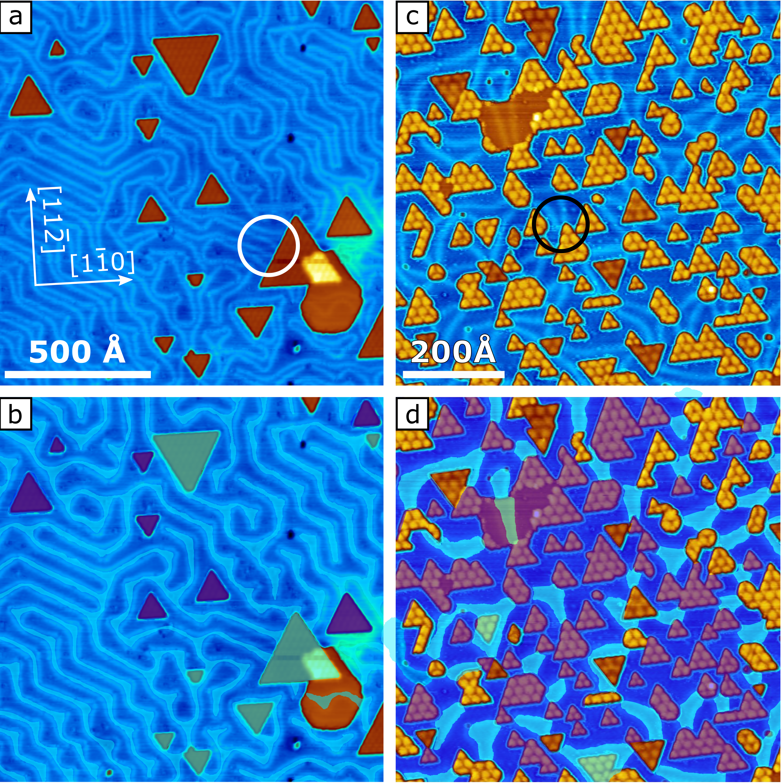
We can sort the tantalum sulfide islands also with respect to the stacking of the Au(111)-substrate. In several of our STM images, the characteristic Au(111)-herringbone reconstruction [18] is visible as a modulation of the blue background. Locally, this reconstruction has the form of parallel bright lines. The majority of the gold atoms is present in the conventional fcc-stacking (larger space between two bright lines), but for a minority, there is a stacking-fault between the topmost and the second layer which induces hcp-type stacking (smaller space between two bright lines).
By analysing the herringbone pattern near tantalum sulfide islands we can determine the stacking of the Au(111)-substrate underneath the tantalum sulfide islands, analogously to the approach of Krane et al. for MoS2/Au(111) [19]. Figure 4 illustrates the matching principle: The original STM-images shown in (a) and (c) are colour-coded in (b) and (d): the fcc areas and correspondingly matched tantalum sulfide islands are marked transparently in dark blue, the hcp areas and matched tantalum sulfide islands in cyan. When the herringbone avoids the island or the lines close at the island edge (usually accompanied by a slight decrease of the hcp herringbone area near the island, see black circle in figure 4 (c)), the island grows on fcc-stacked gold. When the herringbone lines surround the island or the hcp region becomes wider near the island edge (see the white circle in figure 4 (a)), the island grows on hcp-stacked gold.
The experimentally observed distribution for the two criteria ((+)- or (-)-orientation, fcc or hcp substrate stacking) is given in Table 2. We counted several hundred islands, from a full range of preparation conditions. We find an almost equal distribution of the two orientations for TaS2, whereas for TaS the (+)-orientation is strongly favoured. Similarly, we do not observe a strong preference for a specific substrate stacking for TaS2, but TaS islands almost exclusively grow on fcc-stacked Au(111). Taken together, we find that the orientation of both tantalum sulfide phases is linked to the Au(111) surface stacking, the (+)-orientation prefers to grow on fcc-stacked Au areas, whereas the (-)-orientation prefers to grow on the hcp-stacked areas. For TaS, this preference is much more pronounced. The fact that the substrate can imprint its orientation on the TaS much better than on TaS2 indicates that TaS interacts more strongly with its support.
| fcc | hcp | sum | ||
|---|---|---|---|---|
| TaS2 | (+) | 0.42 | 0.03 | 0.45 |
| (-) | 0.11 | 0.44 | 0.55 | |
| sum | 0.53 | 0.47 | ||
| TaS | (+) | 0.95 | 0.00 | 0.95 |
| (-) | 0.00 | 0.05 | 0.05 | |
| sum | 0.95 | 0.05 |
The presence of more than one orientation is detrimental for the application of averaging techniques as angle-resolved photoemission spectroscopy (ARPES) or surface X-ray diffraction (SXRD), as then a superposition of different structures is observed. This can even restore inversion symmetry globally, making special features in the band structure like the opposite spin polarization at the K and K’ points invisible. Growth of single-oriented ultrathin layers is therefore highly desirable. For the related systems MoS2/Au(111) and WS2/Au(111), recipes that lead to a unique orientation have been empirically found [20, 19, 21, 22, 23].
Our growth process highly favours the (+)-orientation for TaS, whereas TaS2 is equally present in both orientations. In the following, we will demonstrate that we can exploit the unique orientation of TaS to reach nearly perfect alignment of TaS2.
We employ a two-step growth process: (i) Growth of TaS ( ML/min, , mbar, K). (ii) Transformation of TaS into TaS2 by annealing in a high H2S atmosphere ( mbar, K). The result of this two step growth process is shown in figure 5. We find extended triangular islands of TaS2. Almost all TaS2 ( %) is present in the (+)-orientation.
This result shows that we can engineer phase and alignment of the tantalum sulfide on Au(111). The orientation of TaS is preserved during the phase change into TaS2. This also indicates that the atomic structure of both phases, including the registry with the substrate, must be closely related. In summary, the growth protocol developed here can be employed in the future for the preparation of TaS2/Au(111) with a unique orientation.
The fact that TaS can be nicely post-sulfurized with key features of the crystal structure staying intact is also interesting with respect to the growth of Janus monolayers of TMDCs where the upper and lower chalcogen layer are different (e.g. Se-Ta-S). There is a lot of interest in this class of 2DMs due to special properties arising from the breaking of in-plane symmetry [24]. We speculate that in our system a two-step growth process as detailed above where in the second step S is replaced by Se or Te, could be a viable pathway towards well-defined Janus membranes.
Now we will go beyond a phenomenological description and link orientation and stacking of the tantalum sulfides to the atomic registry of the islands with respect to the Au(111) substrate.
In general, when a threefold-symmetric 2D-crystal is placed on a sixfold-symmetric substrate, two different orientations related by a rotation by 180∘ are to be expected. For fcc(111), only the first layer is sixfold-symmetric, the subsequent layers reduce this to three-fold symmetry. This can lead to an energetic difference between the two orientations which can result in a reduction or even full suppression of one variant, as has been observed previously for WS2/Ag(111) [25] or hBN/Ir(111) [26, 27].
For Au(111), there is the additional effect of the two different stackings of the substrate. When one only takes the fist two atomic layers into account, the hcp-stacking corresponds to the fcc-stacking with a 180∘-rotation. Therefore, the (+)-orientation on fcc is closely related to the (-)-orientation on hcp, and the (-)-orientation on fcc is closely related to the (+)-orientation on hcp. This is well reflected by our findings summarized in Tab. 2: the fact that the sum of entries on the main diagonal is different from the one on the antidiagonal for both TaS2 and TaS is a clear indication for a significant difference between the dissimilar pairs.
In the following, we focus on the Au(111) fcc stacking, as for TaS2 it is not really necessary to distinguish between the stackings, and for TaS the fcc stacking is the only relevant one. We use the simplified scheme in figure 1. The two possible registries are labelled according to the relative position of Ta and S with respect to the Au substrate as TafccStop and TahcpStop. In explicit, top means that the atoms sit directly on top of an Au in the topmost substrate layer, fcc indicates that the atoms sit at threefold-hollow sites of fcc-type, and correspondingly hcp indicates that the atoms sit at threefold-hollow sites of hcp-type. Conveniently, this nomenclature works for both TaS2 and TaS, one just has to keep in mind that for TaS2, a green circle in figure 1 represents two S, whereas for TaS it represents just one.
The tantalum sulfide islands have two different kinds of edges, the tantalum-terminated Ta-edge and the sulfur-terminated S-edge. Note that we use these terms purely geometrically (i. e. referring to the ideal truncation of the 2D layer) and not chemically. It is well-known that the edges of 2D sulfides are prone to adsorption and reconstruction [28], which is, however, not relevant for our discussion here. In figure 1 we depict the islands as regular hexagons, where Ta- and S-edges have the same length. However, in experiment, this will only be found in special cases, for example, when the islands are in thermodynamic equilibrium with their surroundings and the edge free energies of Ta- and S-edges are the same. If one edge is kinetically or energetically preferred, the islands become more triangular, as indicated in figure 1 by the blue triangles for the assumption of a preference for the Ta-edge. The fact that we observe triangles for both TaS (for small islands) and TaS2 (always) directly indicates that one edge type is indeed preferred. The orientation ((+) or (-)) of the islands is thus directly related to their registry (TafccStop or TahcpStop.) In the following, we want to find this relation, which proves to be notoriously difficult.
Our DFT-calculations show for both phases that TafccStop is energetically preferred (by 2.9 meV and 6.4 meV per tantalum sulfide unit cell for TaS2 and TaS, respectively). Under the assumption that our experimentally observed preference of one orientation is (at least partially) due to energetics, this implies that the (+)-orientation is TafccStop and the (-)-orientation is TahcpStop. There are surely factors beside energetics that determine the island orientation and could in principle even reverse the relation. However, two arguments speak against this in our case: (i) the relation holds for both phases despite their obviously different growth behaviour and (ii) for TaS the energy difference is larger in line with the stronger preference for one orientation found experimentally.
Martincova et al. calculated the energetically preferred shapes of freestanding TaS2 islands under variation of the S chemical potential [29]. Under S-poor conditions, they find a triangular shape exposing solely the Ta-edge. We propose that our growth conditions are indeed S-poor, because our TaS2 islands coexist with the S-deficient TaS-phase. In consequence, our triangular TaS2 islands should be Ta-terminated, as tentatively assumed in figure 1. This again implies that the (+)-orientation is TafccStop and the (-)-orientation is TahcpStop
Based on these two pieces of evidence (energetically preferred TafccStop registry, preferred Ta-edge), in the following, we assume that on fcc-stacked Au(111) the (+)-orientation is TafccStop and the (-)-orientation is TahcpStop. For hcp-stacked Au(111) this relation is reversed. Note that for hcp stacking our nomenclature is used a little bit sloppy: One threefold-hollow side has a Au atom directly below, so we can label this hcp, while the other has a Au atom three layers below due to the stacking fault, but we still label this as fcc.
In our previous paper [11] we chose to display the relaxed structure from DFT for the TahcpStop registry for both TaS2 and TaS in lack of better knowledge on the preferred registry (which turns out to be the opposite one). However, this does not affect any arguments given in this earlier paper.
A slight inconsistency between experiment and theory remains for the case of TaS: The secondary bright area in the moiré unit cell described above (see figure 2 (d)) is found in an up-pointing triangle formed by the primary maxima in experiment. We simulated STM images of this phase (not shown, highly similar to those shown in Ref. [11] for the TahcpStop-registry except for a -rotation). These simulations show a feature of similar appearance, but for the TafccStop-registry this is located in the down-pointing triangles. However, we consider this as a minor problem due to the well-known fallacies of STM simulations (tunneling parameters; tip state) and the potentially simplified geometry we used for the S-poor tantalum sulfide phase in the calculations.
3.2 Boundaries
TaS2 and TaS can form lateral heterostructures as already visible in figure 2 (a). Especially for growth with a high amount of Ta at elevated temperatures, these heterostructures are frequently found, see figure 6, where TaS encompasses TaS2 islands. We observe two different types of boundaries in our system: boundaries between the same phase in different orientations (mirror twin boundary, MTB) and boundaries between different phases (phase boundary, PB).
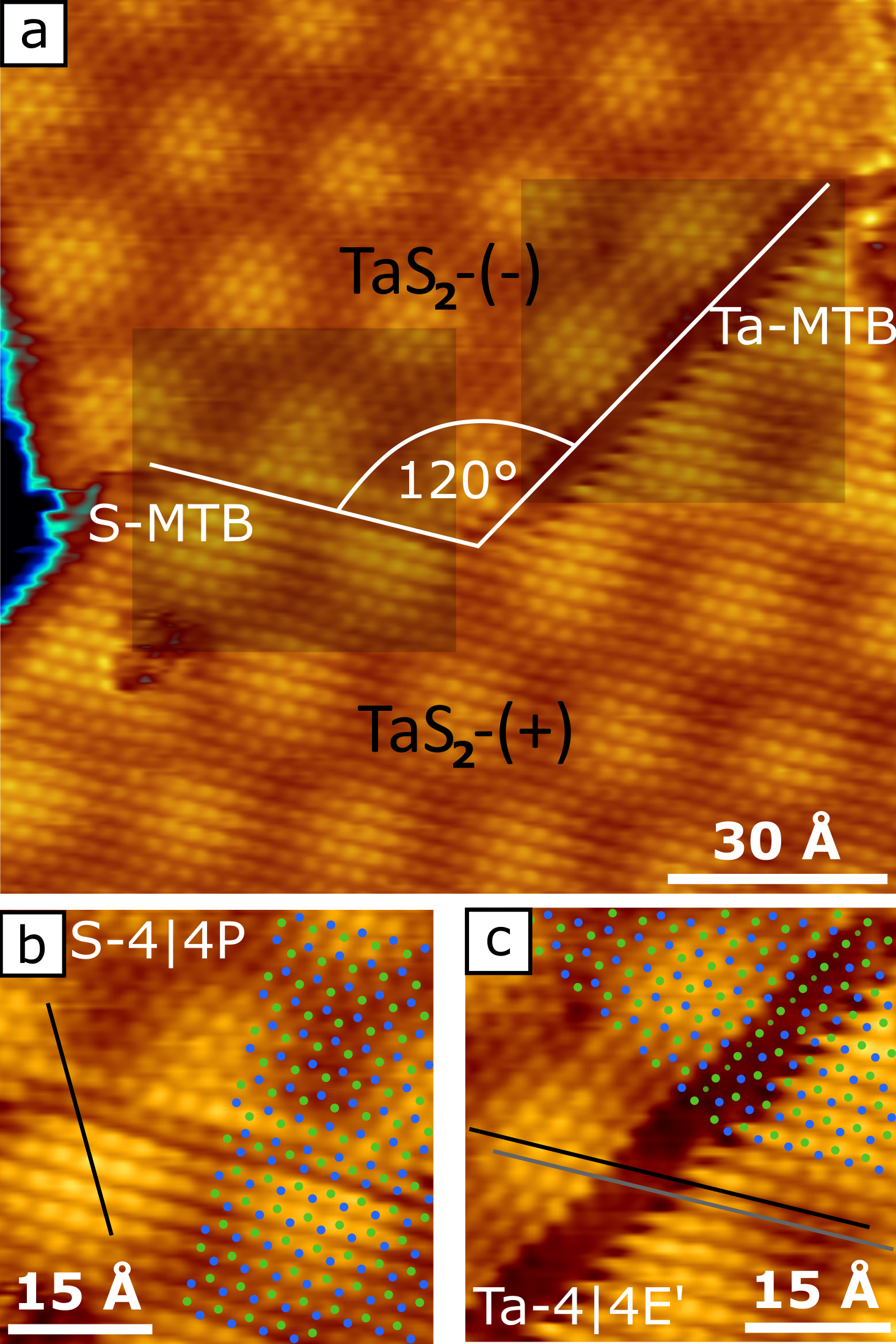
In figure 7 (b) an STM image of two joint TaS2 islands is shown. The two orientations are separated by two domain boundaries, which follow the dense packed rows of the TaS2 atomic lattice. As we do not see a herringbone line emanating from this phase boundary in larger scale images, both islands must reside on the same Au(111) stacking. This is by far the more common situation, and we will focus on this case in the following. Being on the same stacking, the opposite orientation means that the islands have opposite registry. Disregarding the substrate, the two registries are mirror images of each other (see again figure 1). In consequence, the observed domain boundaries are MTBs [30, 31, 32]. We never observe MTBs for TaS, as it only exists in one orientation on a given Au(111) stacking.
The MTBs in figure 7 (a) encompass an angle of , hence one MTB runs along the S- and the other one along the Ta-edge (see again figure 1). A large scale image of the same region shows that the upper part has the (-)-orientation, and the lower part has the (+)-orientation, as already suggested by the small part of the edges visible at the left side of figure 7 (a). With the assumption of Ta-terminated edges motivated above, the right part of the MTB is therefore between Ta-edges (Ta-MTB), and the left part between S-edges (S-MTB).
A magnification of the two MTBs with atomic resolution is shown in figures 7 (b) and (c). The S-MTB (c) shows atomic contrast within the MTB and the atomic rows are aligned even over the MTB (thin black line). For the Ta-MTB (b) we can not resolve the structure within the MTB and the atomic rows are shifted by approximately half a lattice constant when crossing the MTB (black line vs grey line).
The most common MTBs are the high symmetry structures 44P, 44E and 558, which usually are observed along the chalcogen edge [31, 32]. Only very few works report an MTB along the metal edge [33]. Theoretical calculations of MTBs show that the main structural motifs are very similar for different TMDCs [34, 35].
We compare the 44P, 44E and 558 structures to our atomic contrast at the MTBs. For the S-MTB the experimental observations (continued S-rows and atomic resolution in the MTB itself) is reflected best by an S-44P structure (compare structure sketch in figure 7 (b)). The S-44P MTB consists of fourfold rings that meet in a point.
For the Ta-MTB (figure 7 (c)), we find the best agreement for a theoretical structure calculated by Zou et al. [35] and Lehtinen et al. [34], which for simplicity we label 44E’ in the following (compare structure sketch in figure 7 (c)). This structure induces a shift of S atoms by approximately half a lattice constant, in agreement with our experimental observation. Furthermore, in the 44E’ structure there is a hight difference between the central Ta-layers on both sides, and in consequence also for the upper S-layer. This might explain the lack of atomic resolution in experiment. There is no height difference across the boundary for the S-44P MTB. The overlay of the structure model correlates with our atomic contrast, assuming that in agreement with STM simulations, the S-atoms appear bright in STM. The position of MTB is thereby chosen in such a way that the last atomic rows imaged correspond to the S-rows that have the normal (binding) environment in the upper S-layer. MTBs along the metal edge are very rare and to the best of our knowledge, none has been reported for pristine, as-grown TMDCs, yet. A 44E structure along the metal edge has been recently observed for Nb-doped WSe2 [33]. The 44E’ MTB is only theoretically found to be stable but has not been observed experimentally.
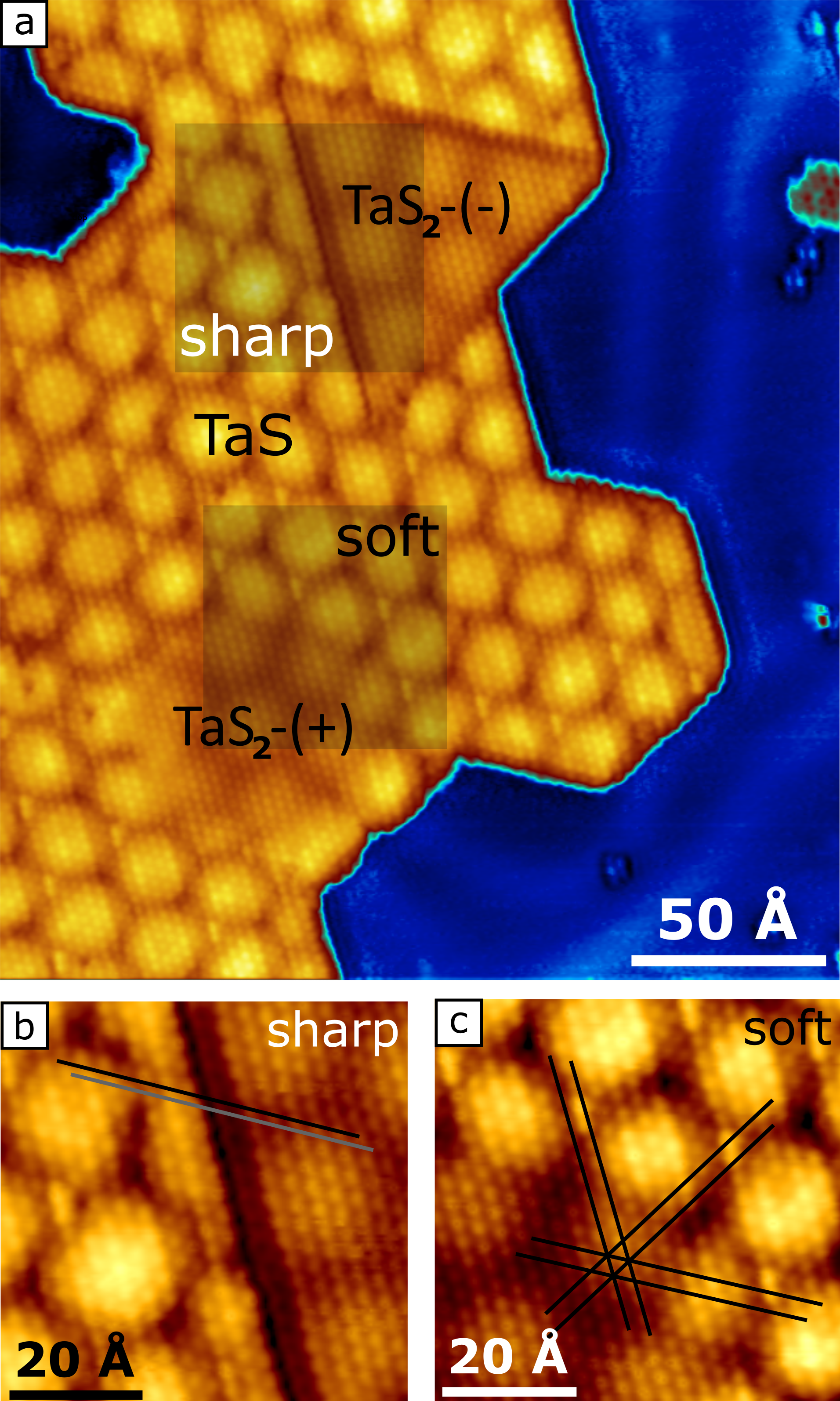
In addition to the mirror twin boundaries between TaS2-(+)- and (-)-domains, we observe PBs between TaS and TaS2, see the STM image in figure 8 (a). These PBs come in two varieties that we label sharp and soft. Soft PBs are always found between TaS2 and TaS islands with the same orientation (almost always TaS2-(+) and TaS-(+)). Sharp PBs form exclusively between TaS2 and TaS with different orientation (almost always TaS2-(-) and TaS-(+)). Also here, we have no indication that islands on the different sides of the boundary reside on different Au(111) stacking. In consequence, the soft boundaries are between TaS2 and TaS in the same registry, while the sharp boundaries are between the different phases in opposite registry.
Figure 8 (a) shows two TaS2 islands embedded in one large TaS island. The TaS2-(+)-island exhibits a soft boundary along all its edges in touch with TaS, the TaS2-(-)-island exhibits a sharp boundary.
The sharp PB can be clearly located (figure 8 (b)). The atomic rows are shifted by approximately half a lattice constant across the boundary (indicated by the thin grey and black lines), similar to what we observed for the Ta-MTB. We interpret the sharp PB as a pseudo-MTB, as here two phases meet that are also mutually rotated by 180∘. It differs from an MTB in the strict sense because of the missing bottom S-layer in TaS.
Figure 8c shows a magnification of the soft PB with atomic resolution. The boundary is so smooth that it is not even clear where the transition from TaS to TaS2 happens exactly. The atomic lattice appears to be completely undisturbed, with continuous alignment of the atomic rows (indicated by the three pairs of parallel black lines). This is true in all directions, hence PBs which form along Ta- and S-edge appear identical in STM. Because of the similar in-plane lattice structure and almost exact match of the lattice parameters of TaS2 and TaS the soft PB appears very smooth and exhibits no obvious defects. We can thus engineer heterostructures of different phases with different properties (e. g. one strongly and one weakly anchored to the substrate) with atomically precise sharp boundaries.
In STM images like figure 6 and 8 (a) TaS2 has a lower apparent height than TaS. This finding holds for a wide range of tunneling conditions. It is counter-intuitive in view of our structural model, see figure 1. We see two solutions for this puzzle: On one hand, as STM always images a convolution of the geometric and the electronic structure, a possible explanation is the different band structure and resulting different local density of states of TaS2 and TaS [11]. Also the opposite direction of charging (electrons flow from the substrate to the overlayer for TaS2, but the other direction for TaS, see table 1) can play a role. In addition, TaS is strongly anchored to the substrate, which may lead to a more 3D-character of its electronic states, and thus to a slower decay of the states into the vacuum. On the other hand, it is also possible that our structural model for TaS is incomplete: Maybe the lower S-layer is not completely absent, or partially replaced by Au. The high mobility of Au atoms at the annealing temperatures combined with the strong interaction between TaS and the substrate may even lead to an accumulation of a full extra gold layer below TaS, which would explain why it is imaged higher in STM.
3.3 Carpet-like growth of TaS2 over Au step edges
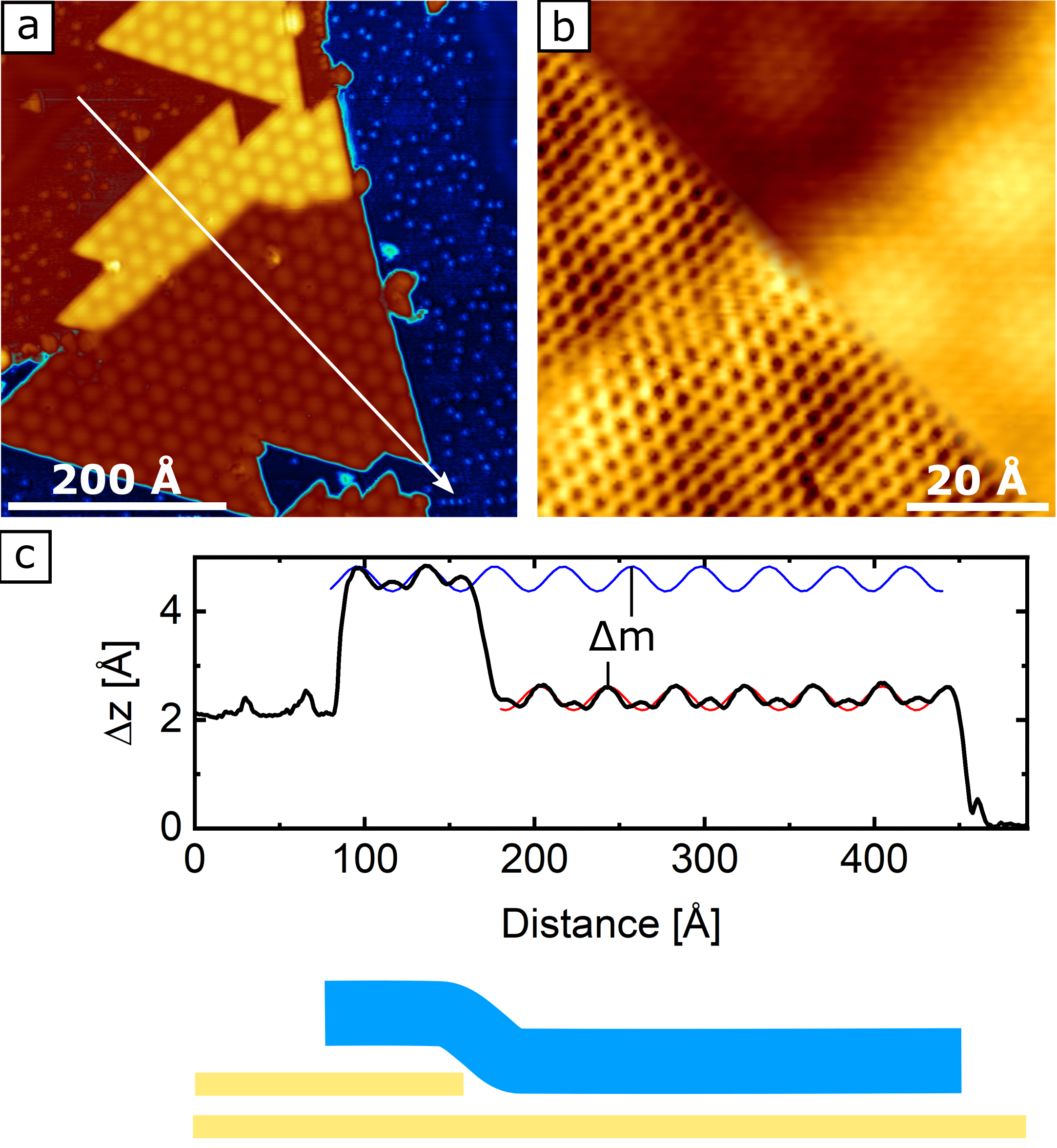
Figure 9 (a) shows a TaS2 island that covers a gold step. The bright yellow part of the island is on the upper gold terrace whereas the darker red-brown part is located on the lower gold terrace. We find that this leads to an atomic lattice that is bent but uninterrupted, as visible in the atomically resolved image shown in figure 9 (b). The upper corner of the image shows the topography image of the step edge with both, the moiré and atomic periodicity resolved. The lower corner shows the same area, but as differentiated STM image, so that the continuity especially of the atomic lattice is better visible. Such growth is already known for several 2D materials [36, 37, 38].
We can determine the bending radius of the 2D-layer when it goes down a substrate step by making use of the magnification effect of the moiré [36]. The smaller the bending radius, the larger the relative shift of the atoms in the lower part from the positions expected by extrapolation from the upper part. While this alone is very difficult to measure, this shift is reflected in a much larger shift of the moire superstructure. Explicitly, they are linked by the expression where is the shift of Au substrate atoms across the step and Å is the Au in-plane lattice constant [39].
We find a moiré shift of Å for {100}-microfacetted steps and Å for {111}-microfacetted steps. This results in a shift of the atoms Å for {100} and AA for {111}. Using the set of two non-linear equations given in Ref. [36], we can estimate the bending radius of the TaS2 sheet to be of the order of 15 - 30 Å. This correlates roughly to the radius of very small group 4 TMDC nanotubes [40].
Because of the asymptotic behaviour of equations towards large bending radii, the error of is significantly larger towards large values than small values of . Furthermore, the model described in Ref. [36] assumes a symmetric bending over the step edge, which for TaS2 (with S-Ta-S sandwich structure) can only be true for the Ta-layer in the middle, the S-layers cannot bend symmetrically. Our analysis thus provides just a rough estimate of the order of magnitude of the bending radius.
For TaS, we regularly find islands that are attached to a gold step edge (e.g. figure 6) but we do not observe TaS islands that grow over a gold step edge like TaS2 does. This observation is in line with a strong substrate interaction.
4 Conclusion
Using the same ingredients, two different phases of monolayer tantalum sulfide can be grown on Au(111). The conventional 2H-TaS2 and the sulfur deficient TaS2-x with (called TaS in this paper). For both phases we typically find triangular islands that can be present in two orientations on Au(111) linked by a -rotation and that can be found on both fcc-stacked and hcp-stacked areas within the Au(111) herringbone reconstruction. While 2H-TaS2 does not show a clear preference both for orientation and substrate stacking, TaS prefers to grow on fcc-stacked gold in just one orientation. We can exploit this for phase engineering, where we transform highly oriented TaS by post-sulfurization into highly oriented 2H-TaS2. Thereby, the breaking of inversion symmetry is globally preserved and enables, among other things, the detection of spin-split valleys at the inequivalent K points by ARPES.
Under the assumption that the edges of the triangular islands are terminated by Ta for both 2H-TaS2 and TaS and that the energetically preferred orientations prevail, we can fully determine the registry of both phases with the substrate for all orientations and both stackings. The TafccStop-registry is preferred for both phases.
For higher coverages we find mirror twin boundaries between differently oriented domains of 2H-TaS2, both along the Ta-edges and the S-edges. We identify them as 44P for the S-MTB and 44E’ for the Ta-MTB. In addition we find heterostructures between the different phases. When both phases have the same orientation, these boundaries are atomically sharp and smooth. We are thus able to coherently join materials with different properties.
2H-TaS2 shows a carpet-like growth over step edges of Au(111). We determine the bending radius of the monolayer across the step to be of the order of 15 to 30 Å, which relates to thin TMDC nanotubes.
References
References
- [1] Y. Chen, Z. Lai, X. Zhang, Z. Fan, Q. He, C. Tan, and H. Zhang. Phase engineering of nanomaterials. Nat. Rev. Chem., 4:243, 2020.
- [2] R. Wang, Y. Yu, S. Zhou, H. Li, H. Wong, Z. Luo, L. Gan, and T. Zhai. Strategies on Phase Control in Transition Metal Dichalcogenides. Adv. Funct. Mater., 28:1802473, 2018.
- [3] M. Bonilla, S. Kolekar, J. Li, Y. Xin, P. M. Coelho, K. Lasek, K. Zberecki, D. Lizzit, E. Tosi, P. Lacovig, S. Lizzit, and M. Batzill. Compositional Phase Change of Early Transistion Metal Diselenide (VSe2 and TiSe2) Ultrathin Films by Postgrowth Annealing. Adv. Mater. Interfaces, 7:2000497, 2020.
- [4] X. Zhao, P. Song, Wang. C., A. C. Riis-Jensen, W. Fu, Y. Deng, D. Wan, L. Kang, S. Ning, J. Dan, T. Venkatesan, Z. Liu, W. Zhou, K. S. Thygesen, X. Luo, S. J. Pennycook, and K. P. Loh. Engineering Covalently Bonded 2D Layered Materials by Self-Intercalation. Nature, 581:171, 2020.
- [5] F. Arnold, R.-M. Stan, S. K. Mahatha, H. E. Lund, D. Curico, M. Dendzik, H. Bana, E. Travaglia, L. Bignardi, P. Lacovig, D. Lizzit, Z. Li, M. Bianchi, J. Miwa, M. Bremholm, S. Lizzit, P. Hofmann, and C. E. Sanders. Novel Single-Layer Vanadium Sulphide Phases. 2D Mater., 5:045009, 2018.
- [6] F. Cheng, Z. Ding, H. Xu, S. J. R. Tan, I. Abdelwahab, J. Su, P. Zhou, J. Martin, and K. P. Loh. Epitaxial Growth of Single-Layer Niobium Selenides with Controlled Stoichiometric Phases. Adv. Mater. Interfaces, 5:1800429, 2018.
- [7] M. Chhowalla, H. S. Shin, G. Eda, L. J. Li, K. P. Loh, and H. Zhang. The chemistry of two-dimensional layered transition metal dichalcogenide nanosheets. Nat. Chem., 5:263–275, 2013.
- [8] C. E. Sanders, M. Dendzik, A. S. Ngankeu, A. Eich, A. Bruix, M. Bianchi, J. A. Miwa, B. Hammer, A. A. Khajetoorians, and P. Hofmann. Crystalline and Electronic Structure of Single-Layer TaS2. Phys. Rev. B, 94:081404, 2016.
- [9] D. Xiao, G.-B. Liu, W. Feng, X. Xu, and W. Yao. Coupled Spin and Valley Physics in Monolayers of MoS2 and Other Group-VI Dichalocogenides. Phys. Rev. Lett., 108:196802, 2012.
- [10] F. Jellinek. The System Tantalum-Sulfur. J. Less Common Met., 4:9–15, 1962.
- [11] D. Dombrowski, A. Samad, C. Murray, M. Petrović, P. Ewen, T. Michely, M. Kralj, U. Schwingenschlögl, and C. Busse. Two Phases of Monolayer Tantalum Sulfide on Au(111). ACS Nano, 15:13516, 2021.
- [12] C. C. Silva, D. Dombrowski, A. Samad, J. Cai, W. Jolie, J. Hall, P. T. P. Ryan, P. K. Thakur, D. A. Duncan, T.-L. Lee, U. Schwingenschlögl, and C. Busse. Structure of monolayer 2H-TaS2 on Au(111). Phys. Rev. B, 104:205414, 2021.
- [13] G. Kresse and D. Joubert. From ultrasoft pseudopotentials to the projector augmented-wave method. Phys. Rev. B, 59:1758, 1999.
- [14] J. P. Perdew, K. Burke, and M. Ernzerhof. Generalized gradient approximation made simple. Phys. Rev. Lett., 77:3865, 1996.
- [15] S. Grimme. Semiempirical GGA-Type Density Functional Constructed with a Long-Range Dispersion Correction. J. Comput. Chem., 27:1787, 2006.
- [16] J. Tersoff and D. R. Hamann. Theory of the scanning tunneling microscope. Phys. Rev. B, 31:805–813, 1985.
- [17] M. Yu and D. R. Trinkle. Accurate and efficient algorithm for Bader charge integration. J. Chem. Phys., 134:064111, 2011.
- [18] J. V. Barth, H. Brune, and G. Ertl. Scanning Tunneling Microscopy Observations on the Reconstructed Au(111) Surface: Atomic Structure, Long-Range Superstructure, Rotational Domains, and Surface Defects. Phys. Rev. B, 42:9307, 1990.
- [19] N. Krane, C. Lotze, and K. J. Franke. Moiré structure of MoS2 on Au(111): Local structural and electronic properties. Surf. Sci., 678:136, 2018.
- [20] H. Bana, E. Travaglia, L. Bignardi, P. Lacovig, C. E. Sanders, M. Dendzik, M. Michiardi, M. Bianchi, D. Lizzit, F. Presel, D. De Angelis, N. Apostol, P. K. Das, J. Fujii, I. Vobornik, R. Larciprete, A. Baraldi, P. Hofmann, and S. Lizzit. Epitaxial growth of single-orientation high-quality MoS2 monolayers. 2D Mater., 5:035012, 2018.
- [21] F. Tumino, C. S. Casari, A. L. Bassi, M. Passoni, and V. Russo. Pulsed laser deposition of single-layer MoS2 on Au(111): from nanosized crystals to large-area films. Nanoscale Adv., 1:643, 2019.
- [22] H. Beyer, G. Rohde, A. Grubišić Čabo, A. Stange, T. Jacobsen, L. Bignardi, D. Lizzit, P. Lacovig, C. E. Sanders, S. Lizzit, K. Rossnagel, P. Hofmann, and M. Bauer. 80% Valley Polarization of Free Carriers in Singly Oriented Single-Layer WS2 on Au(111). Phys. Rev. Lett., 123:236802, 2019.
- [23] L. Bignardi, D. Lizzit, H. Bana, E. Travaglia, P. Lacovig, C. E. Sanders, M. Dendzik, M. Michiardi, M. Bianchi, M. Ewert, L. Buß, J. Falta, J. I. Flege, A. Baraldi, R. Larciprete, P. Hofmann, and S. Lizzit. Growth and structure of singly oriented single-layer tungsten disulfide on Au(111). Phys. Rev. Mater., 3:014003, 2019.
- [24] A.-Y. Lu, H. Zhu, J. Xiao, C.-P. Chuu, Y. Han, M.-H. Chiu, C.-C. Cheng, C.-W. Yang, K.-H. Wei, Y. Yang, Y. Wang, D. Sokaras, D. Nordlund, P. Yang, D. A. Muller, M.-Y. Chou, X. Zhang, and L.-J. Li. Janus monolayers of transition metal dichalcogenides. Nature Nanotechnology, 12:744, 2017.
- [25] S. Ulstrup, A. Grubišić Čabo, D. Biswas, J. M. Riley, M. Dendzik, C. E. Sanders, M. Bianchi, C. Cacho, D. Matselyukh, R. T. Chapman, E. Springate, P. D. C. King, J. A. Miwa, and P. Hofmann. Spin and valley control of free carriers in single-layer WS2. Phys. Rev. B, 95:041405, 2017.
- [26] F. Orlando, P. Lacovig, N. G. Omiciuolo, L. Apostol, R. Larciprete, A. Baraldi, and S. Lizzit. Epitaxial Growth of a Single-Domain Hexagonal Boron Nitride Monolayer. ACS Nano, 8:12063, 2014.
- [27] F. H. Farwick zum Hagen, D. M. Zimmermann, C. C. Silva, C. Schlueter, N. Atodiresei, W. Jolie, A. J. Martínez-Galera, D. Dombrowski, U. A. Schröder, M. Will, P. Lazić, V. Caciuc, S. Blügel, T.-L. Lee, T. Michely, and C. Busse. Structure and Growth of Hexagonal Boron Nitride on Ir(111). ACS Nano, 10:11012, 2016.
- [28] J. V. Lauritsen, J. Kibsgaard, S. Helveg, H. Topsøe, B. S. Clausen, E. Lægsgaard, and F. Besenbacher. Size-dependent structure of MoS2 nanocrystals. Nat. Nanotechnol., 2:53, 2007.
- [29] J. Martincová, M. Otyepka, and P. Lazar. Atomic-Scale Edge Morphology, Stability and Oxidation of Single-Layer 2H-TaS2. ChemPlusChem, 85:2557, 2020.
- [30] A. M. van der Zande, P. Y. Huang, D. A. Chenet, T. C. Berkelbach, Y. You, G.-H. Lee, T. F. Heinz, D. R. Reichman, D. A. Muller, and J. C. Hone. Grains and grain boundaries in highly crystalline monolayer molybdenum disulphide. Nat. Mater., 12:554, 2013.
- [31] H.-P. Komsa and A. V. Krasheninnikov. Engineering the Electronic Properties of Two-Dimensional Transition Metal Dichalcogenide by Introducing Mirror Twin Boundaries. Adv. Electron. Mater., 3:1600468, 2017.
- [32] M. Batzill. Mirror twin grain boundaries in molybdenum dichalcogenides. J. Phys. Condens. Matter, 30:493001, 2018.
- [33] B. Wang, Y. Xia, J. Zhang, H.-P. Komsa, M. Xie, Y. Peng, and C. Jin. Niobium doping induced mirror twin boundaries in MBE grwon WSe2 monolayers. Nano Res., 13:1889, 2020.
- [34] O. Lehtinen, H.-P. Komsa, A. Pulkin, M. B. Whitwick, M.-W. Chen, T. Lehnert, M. J. Mohn, O. V. Yazyev, A. Kis, U. Kaiser, and A. V. Krasheninnikov. Atomic Scale Microstructure and Properties of Se-Deficient Two-Dimensional MoSe2. ACS Nano, 9:3274, 2015.
- [35] X. Zou and B. I. Yakobson. Metallic High-Angle Grain Boundaries in Monolayer Polycrystalline WS2. Small, 11:4503, 2015.
- [36] J. Coraux, A. T. N’Diaye, C. Busse, and T. Michely. Structural Coherency of Graphene on Ir(111). Nano Lett., 8:565, 2008.
- [37] S. G. Sørensen, H. G. Füchtbauer, A. K. Tuxen, A. S. Walton, and J. V. Lauritsen. Structure and Electronic Properties of in Situ Synthesized Single-Layer MoS2 on a Gold Surface. ACS Nano, 8:6788, 2014.
- [38] M. Dendzik, M. Michiardi, C. E. Sanders, M. Bianchi, J. A. Miwa, S. S. Grønborg, J. V. Lauritsen, A. Bruix, B. Hammer, and P. Hofmann. Growth and electronic structure of epitaxial single-layer WS2 on Au(111). Phys. Rev. B, 92:245442, 2015.
- [39] A. Maeland and T. B. Flanagan. Lattice spacings of gold–palladium alloys. Can. J. Phys., 42:2364, 1964.
- [40] M. Nath and C. N. R. Rao. New Metal Dislufide Nanotubes. J. Am. Chem. Soc., 123:4841, 2001.