A quantum dot-based frequency multiplier
Abstract
Silicon offers the enticing opportunity to integrate hybrid quantum-classical computing systems on a single platform. For qubit control and readout, high-frequency signals are required. Therefore, devices that can facilitate its generation are needed. Here, we present a quantum dot-based radiofrequency multiplier operated at cryogenic temperatures. The device is based on the non-linear capacitance-voltage characteristics of quantum dot systems arising from their low-dimensional density of states. We implement the multiplier in a multi-gate silicon nanowire transistor using two complementary device configurations: a single quantum dot coupled to a charge reservoir and a coupled double quantum dot. We study the harmonic voltage conversion as a function of energy detuning, multiplication factor and harmonic phase noise and find near ideal performance up to a multiplication factor of 10. Our results demonstrate a method for high-frequency conversion that could be readily integrated into silicon-based quantum computing systems and be applied to other semiconductors.
I Introduction
Quantum dots (QDs) show great promise as a scalable platform for quantum computation [1] following the recent demonstrations of universal control of 4- and 6-qubit systems [2, 3] and the scaling to 4x4 QD arrays [4]. Quantum dots in silicon as a host for spin qubits are particularly attractive due to the demonstrated high-fidelity control [5, 6, 7], industrial manufacturability [8, 9], co-integration with classical cryogenic electronics [10, 11, 12] and the availability of detailed proposals for large-scale integration [13, 14, 15, 16, 17, 18, 19].
As QDs become an established platform for qubit implementation, novel ways of operating such devices are beginning to emerge, providing an opportunity to integrate on the same embodiment additional functionalities. In particular, by exploiting the non-linear high-frequency admittance, QDs can be utilised as compact charge sensors [20, 21], fast local thermometers [22, 23] or as parametric amplifiers [24] for quantum-limited amplification. Here, we present a new functional implementation: a quantum dot-based radio-frequency multiplier.
A frequency multiplier typically consists of a non-linear circuit element which distorts a sinusoidal signal, generating multiple harmonics. A band-pass filter is then used to select a particular harmonic. Commercially, this can be achieved by utilising, for example, semiconductor-based diodes or amplifiers but these dissipate energy reducing their power conversion performance. Alternatively, microelectromechanical resonators can be utilised for multiplication with enhanced performance due to their low-loss nature [25].
In this manuscript, we propose and demonstrate a QD-based radio-frequency multiplier in silicon. We demonstrate frequency multiplication on a single device in two complementary configurations: a single QD couple to a reservoir and a double QD. Due to the non-dissipative nature of the device impedance under elastic tunnelling conditions, the devices show near-ideal power conversion and phase-noise properties for a multiplication factor of up to 10. Such devices could be utilised to alleviate the challenges associated with the delivery of high-frequency signals to quantum processors from room temperature down to cryogenic stages in dilution refrigerators while reducing the cost and complexity of the room temperature electronics.
II QD frequency multiplication:
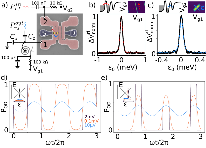
The device used to demonstrate frequency multiplication is the same as in ref. [20]. It consists of a fully-depleted silicon nanowire transistor with four wraparound gates in series, as shown in Fig. 1a. Quantum dots form under the gates at cryogenic temperatures when biased close to the threshold voltage [26]. In this demonstration, we utilise voltages on gate 1 () and 2 () to form either a QD coupled to a reservoir or a double QD. Further, we apply a radio-frequency (rf) signal via gate 2 and then measure the transmission through the QD system at the output of an lumped-element resonator connected to gate 1, which acts as a high-quality band-pass filter around its natural frequency, MHz. Changes in transmitted voltage through the setup are directly proportional to the device’s admittance and since in QD systems, it is a highly nonlinear function of the gate voltage [27, 28, 29, 30, 31, 32], they can be utilised for frequency multiplication when driven beyond its linear regime, as we shall see.
We now explain the non-linearity of QD systems in detail. The non-linear admittance arises from the dependence of the gate charge () with gate voltage. More particularly, for a QD coupled to a reservoir in the fast relaxation regime, , where is the charge tunnelling rate, the gate charge reads
| (1) |
where is the electron occupation probability, is the Fermi-Dirac probability distribution, the Boltzmann constant, the charge of an electron and the system temperature. Here is the detuning between the QD electrochemical level and the Fermi level at the reservoir, is the voltage at which these two levels are aligned and is the gate lever arm to dot [22] for . In the case of a double quantum dot (DQD), in the adiabatic limit, the gate charge is
| (2) |
where in this case refers to the energy detuning between QDs, to the ICT lever arm, and is the tunnel coupling [30]. When subject to the oscillatory detuning [] due to the rf excitation, an oscillatory gate current flows through the system proportional to its admittance
| (3) |
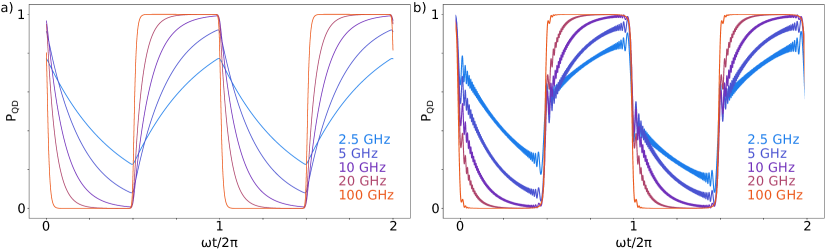
Changes in device admittance occur either due to dot-to-reservoir (DTR) charge transition, as shown in Fig. 1b or inter-dot-charge transitions (ICTs), depicted in Fig. 1c with their corresponding fits using the calculated admittance. If the rf excitation is small (), the DTR or ICT respond linearly to the input voltage. In this regime, the charge oscillates at the rf frequency, with a phase shift dependent on the magnitude of the Sisyphus resistance [31], see blue traces in Fig. 1(d,e). When driving the systems beyond their linear regime, the charge distribution gets distorted as the QD is either filled or emptied. As long as remains smaller than the charging energy, the system is required to obey at all times. Eventually, in the large-signal regime (), acquires a square wave-like response containing high-frequency harmonics of the original signal, see Fig. 1d,e and Appendix A. Comparing Eq. 1 and Eq. 2, we note how the DTR depends exponentially on , while is a polynomial function. Therefore, we expect the DTR to show a higher degree of non-linearity than the ICT in the intermediate signal regime, as we shall see.
Following the derivation in Appendix B, we can then express the rf voltage output at the -th harmonic, , in terms of the -th harmonic of the gate current and hence that of the charge occupation probability,
| (4) |
For a DTR with tunnel rate , a simple analytical solution can be found for the output voltage at the -th harmonic,
| (5) |
where we define as
For the ICT, there is no simple general analytical solution for the output voltage, equivalent to Eq. (4) (see Appendix A). However, using a semiclassical approach, we derive a simple expression for the driven probability distribution. In the regime of fast relaxation, i.e. , where is the coupling rate to the phonon bath, absorption and emission mix the ground and excited states, driving them to thermal equilibrium faster than the basis rotation caused by the rf perturbation [31]. If we define , with being the Bose-Einstein distribution, we find a simple expression for the driven probability distribution
| (6) |
Equation (6) presents the same large-signal square-wave limit discussed thus far but with a different response to the DTR in the intermediate regime. We note the equation is valid in the limit of , where the evolution can be considered adiabatic.
Finally, we find that in the large signal regime, (), both systems, QD and DQD, produce an output voltage given by
| (7) |
which unifies the large-signal response of the DTR and ICT as it only depends on and and not on the physical characteristics of the particular quantum systems. Equation (7) also highlights that the maximum voltage conversion at the -th harmonic follows a trend, which translates into the maximum trend for the well-known maximum power conversion efficiency of an ideal frequency multiplier. Further, we note that the detuning offset, , changes the duty cycle of the square-like output wave (see Appendix A) as we vary the probability of the QD being filled or emptied, as shown in Fig. 1e. Accordingly
| (8) |
if , while the QD remains trivially empty or full if never changes sign. The offset detuning dependence of , and thus , enables changing the relative amplitude of the spectral components of the voltage output, as we shall see.
III Experimental Results
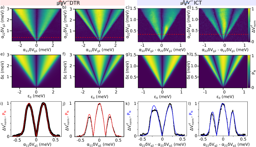
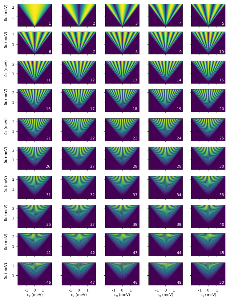
Equation (4) shows how large rf perturbations can be used to demonstrate a QD-based frequency multiplier. Due to the fixed resonance frequency of our resonator (789 MHz), which acts as a sharp band-pass filter (see Appendix C), we fix the output frequency by setting the local oscillator (LO) used for homodyne mixing at . To probe the various harmonics, we perturbed the system via an rf signal along gate 2 at integer fractions of the resonator’s frequency . In Fig. 2, we show how the second and third harmonics evolve as a function of driving and detuning offset for a DTR and an ICT. We observe that all harmonics are symmetric along zero detuning (up to a phase of ) and are characterised by lobes in the magnitude response signal. For the even harmonics, the maximum voltage transferred occurs at and is zero at (see Appendix D). In contrast, for the odd harmonics, the signal is maximum at . As a result, the optimum detuning point to operate frequency multiplication varies for the different harmonics.
To accurately simulate the line-shape response for the various harmonics for both DTRs and ICTs, we developed a Lindblad framework. The method entails iterating the Lindblad Master Equation [33], defined as
| (9) |
with
| (10) |
to numerically obtain the QD occupation probability . Combined with Eq. 4, it allows us to simulate the rf reflectometry lineshapes without making use of the approximations in Eqs. (1) and (2). A mathematical derivation of the jump operators and their relative relaxation rates for the DTR and the ICT can be found in Appendix E. The gate lever arms ( and ) and electron temperature ( mK) were extracted experimentally in the small signal regime (see Appendices F- G), leaving the reservoir-dot relaxation rate and the double QD tunnel coupling as fitting parameters. Because of the different capacitive coupling between gates at high frequency, we estimate from the data the high-frequency lever arm of G2 on the QD along the DTR, with a value of . With these values, we use lineshapes at constant rf power (Fig. 2(i-l)) to fit GHz and the ICT tunnel coupling eV.
Comparing Fig. 2(i-l), we notice the stark similarity of the lineshapes of the DTR and ICT in the large-signal regime ( meV), which can be attributed to the same square-wave-like behaviour of Eq. (1) and Eq. (2). We see, however, slightly more pronounced sidebands in the ICT at the 3 harmonic when compared to the DTR. We attribute this to the lifetime-broadening of the DTR (see Fig. 9 in Appendix G), whose model (red line) shows excellent agreement with the experimental data. Moreover, comparing the data with the fits (blue lines) for the ICT, we observe an asymmetry with respect to , which is not present in the theory. We attribute this effect to not having swept the gate voltages perfectly along the detuning axis due to the difference in lever arms between G1 and G2.
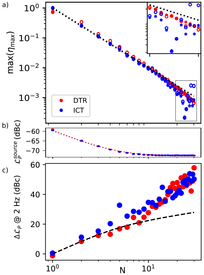
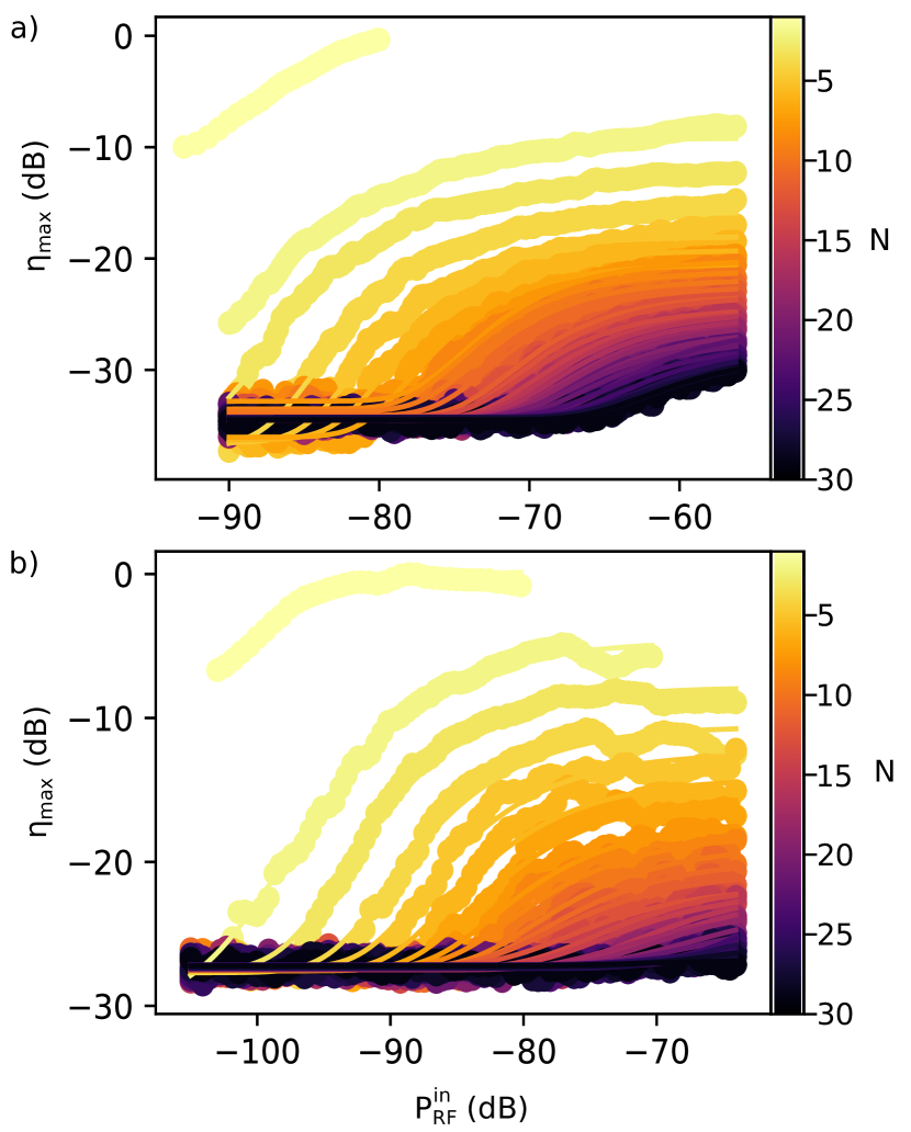
We now move on to assess the performance of the QD-based frequency multiplier. First, we investigate the harmonic power conversion efficiency by rf voltage output maps equivalent to those shown in Fig. 2 up to /50 (Appendices H- I). We quantify this efficiency by defining the figure of merit
| (11) |
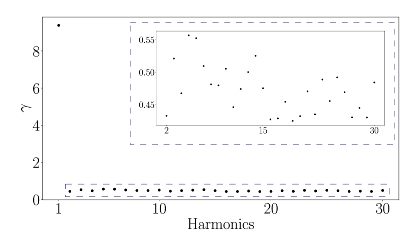
where indicates the measured output voltage at the harmonic. We chose this metric as it accounts for losses along the rf lines. We take the maximum signal for a given rf input power, as the detuning for optimal conversion, which depends on the specific harmonic of interest (Fig. 2). At /50, a weak signal is still discernible for the DTR transitions but not for the ICTs, which we detect up to /30. We then extract the power conversion efficiency for the different harmonics at a given input power (Appendix J). In Fig. 3a, we plot the maximum power conversion efficiency compared to the first harmonic for the DTR and the ICT. The maximum power conversion efficiency follows the expected dependence for a square wave (black dotted line) until /20, above which max() begins to drop below the trend, as highlighted by the insert. We attribute lower power conversion efficiency observed at higher harmonics to the signal not being fully saturated at the maximum rf power used to probe the device. The ICT diverges from the dependence more drastically than the DTR due to a combination of factors. Firstly, being unable to drive the system as hard before excited states and multiple charge transitions start interfering (see Appendix K). Secondly, there is a decrease in signal due to the less-pronounced non-linearity for an ICT compared to a DTR transition (see Appendices H-I).
Another important metric for frequency multiplication is to assess the increase in phase noise at higher harmonics. To calibrate our system, we measure the phase noise of the rf source, , (Fig. 3b) at the frequencies used to drive the DTR and ICT. The decrease in phase noise as we decrease the excitation frequency () follows the empirically established Leeson’s equation [34] (red dotted line).
In Fig 3c, the data shows the phase noise contribution of the QD-based frequency multiplier, , obtained by subtracting the rf source phase noise from the total phase noise measured. The harmonics produced by the driven QD system have an increasing phase noise as a function of the multiplication factor. Up to 10, the phase noise of our system is ideal (black dotted line), as defined in Appendix L, above which, it diverges. The exact reason is unknown but we speculate that it is due to the output signal not being fully saturated. In this regime, additional phase noise may arise due to charge noise since the system is more sensitive to charge probability variations as the occupation probability is not in a square-wave-like regime.
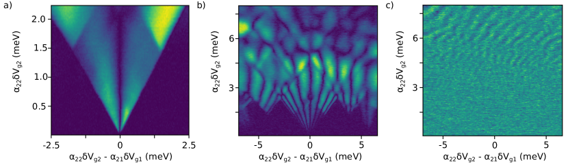
Finally, we examine the performance of the multiplier when multiple charge transitions begin to merge above a given driving power, (). In Fig. 4a, we explore . We observe that at an excitation amplitude meV, neighbouring DTR lines begin to interfere; as two electrons are being loaded and unloaded in phase from the QD. Due to the -1 nodes present in the phase of the -th harmonic, constructive and destructive interference can occur, which can give rise to an increase in signal proportional to the number of tunnelling electrons involved in the process, resulting in max() exceeding the expected dependence. Within this regime, the two-level system framework developed in Appendices A and B is no longer valid. Therefore, the data in this regime was omitted from the max() and discussion. We also observe the same interference behaviour for the ICT, with the added phenomenon of having excited states appearing at certain driving rf powers, as outlined in Appendix K. Although harder to interpret, these regions of interference allow higher harmonics to be measured. We detected rf output signals up to (Appendix K).
IV Conclusions and outlook
We have introduced the idea of a quantum-dot based frequency multiplier and demonstrated its experimental implementation via two methods: a QD coupled to a reservoir, and a double QD. We find near-ideal performance in terms of power conversion and phase noise up to . The device may facilitate generating on chip the high-frequency signal needed for qubit control ( GHz) [35, 36] and readout (0.1-2 GHz) [37] by operating it in conjunction with a lower frequency generator. Such an approach may help preserve signal integrity from room temperature down to the mixing chamber of a dilution refrigerator and/or may facilitate the development of an integrated cryogenic frequency generator. Furthermore, if combined with frequency mixing [38, 39, 40] and parametric amplification [24], one may envision an all QD-based rf reflectometry setup including frequency generation, amplification and mixing.
With regard to the performance, we expect near-ideal properties as long as the electron tunnelling process on which the operation of the multiplier is based remains elastic. This condition sets upper bounds for the maximum input frequency to in the DTR case, and for the ICT. The device remains operational at higher frequencies but additional dissipation may deteriorate its performance. Finally, we note that the large-signal regime explored here can be utilised for excited state spectroscopy of (D)QD systems.
V Acknowledgements
This research was supported by European Union’s Horizon 2020 research and innovation programme under grant agreement no. 951852 (QLSI), and by the UK’s Engineering and Physical Sciences Research Council (EPSRC) via the Cambridge NanoDTC (EP/L015978/1), QUES2T (EP/N015118/1), the Hub in Quantum Computing and Simulation (EP/T001062/1) and Innovate UK [10000965]. M.F.G.Z. acknowledges a UKRI Future Leaders Fellowship [MR/V023284/1].
Appendix A Occupation in the large-signal regime
The naive solution to the (D)QD occupation in the large signal regime would be to assume a square-wave-like behaviour, where the (D)QD is periodically emptied and filled if the rf amplitude is much larger than the detuning. This ansatz, however, fails due to the finite relaxation times of the respective systems. For the DTR, we can find an analytical expression for the large-signal regime through the Master Equation in Eq. (35), whose solution at the steady-state is
| (12) |
which can be expressed as the Fourier series
| (13) |
where
is the -th Fourier component of the perturbed Fermi-Dirac. In the limit of fast relaxation (), Eq. 13 simplifies to , which indeed tends to a square wave for large driving. For the coupling to the reservoir behaves as a low pass filter for the square wave (see Fig. 5(a)). In our particular experimental setup we have a fixed resonator, thus is constant. Therefore, the prefactor
is just a global constant for all harmonics and all powers, thus all the dynamics is described by , which is square-wave-like.
For the ICT, we can consider a semiclassical solution in which the system evolves while remaining in the ground state. This represents the behaviour of the ICT if the tunnel coupling is large enough to neglect Landau-Zener transitions (i.e. ) [41] and relaxation events (i.e. ). In this case, we can simply write:
| (14) |
where is the probability of the electron occupying the QD under the input gate. In the large-signal regime (i.e. ), it is clear that tends to a square wave as the charge shifts from one QD to the other.
When considering the full model from the LME, we find the possible presence of Landau-Zener transitions when , which produce oscillations at the Rabi frequency . The result of these two effects produces a which is formally no longer a square wave. However, we can gain insight into the effect of phonon relaxation in the system by considering the semiclassical approximation of the LME. In the basis where is instantaneously diagonal (i.e. the energy basis), this reads
| (15) |
whose formal solution is
| (16) |
where we defined
| (17) |
Projecting back into the QD basis, we can write
| (18) | |||
where indicates the -th Fourier component of the convolution of the two Fourier series. Comparing the formal similarity Eqs. (12) and (16), we can infer that the two systems will have comparable responses to increasing relaxation rate. More thoroughly, it is possible to put a boundary on the effect of relaxation by considering that . In particular, in the large-signal , is meaningfully different from zero only on the points in the cycle where . Therefore, the effect of the convolution is to add a finite slew rate to the square-wave-like response of . Therefore, we ought to be able to neglect the effects of , recovering the exact equivalence of the ICT with the DTR. This is highlighted in Fig. 5(b), which shows how the behaviour of the ICT remains qualitatively similar to that of the DTR when including relaxation and for varying . Moreover, we can see the fast oscillations at the Rabi frequency, which cannot be captured by the semiclassical nature of the Master Equation in Eq. 15.
Following Eq. (14), in the large-signal regime, we expect the main difference between the ICT and the DTR to be, apart from global constants, the substitution of with . The fact that the latter is a polynomial function of energy, explains the lower degree of non-linearity observed for the ICT when compared with the exponential behaviour of the Fermi-Dirac in the DTR.
Moreover, for both systems, the square-wave behaviour can be written as the Heaviside theta . Therefore, if , it is trivial to predict the duty cycle as
| (19) |
Appendix B Reflectometry Lineshapes
Rf reflectometry measures charge transitions via changes in the reflection coefficient of a quantum system. In this work, we measured the transmission line-shapes from G2 to G1, as detailed in Fig. 1. We can write the transmission coefficient as
| (20) |
where is the characteristic impedance of the line. is the effective admittance of the quantum system, where we can assume . The quantum admittance can be modelled as the charge-dependent equivalent to the Quantum Capacitance and Sisyphus resistance. For a particular harmonic , the quantum admittance is defined as
| (21) |
where is the -th Fourier Component of the current through the device. Therefore, we can calculate the output of the rf measurement as
| (22) | |||
| (23) |
Therefore, we can compute the rf lineshapes of by either numerically iterating the LME or from the expressions in Appendix A.
We must be aware that the above theory assumes a 0D discrete level with a delta-like density of states. In the case of the DTR, however, the coupling with the reservoir broadens the level. This can be modelled with an effective Lorentzian density of states with full-width half-maximum . This lifetime-broadening becomes important when and can be accounted for considering the convolution of for the delta-like level with . The DTR of interest in this work is lifetime-broadened, as discussed in Appendix G; therefore, this correction was used to fit the maps in Fig 11, with an estimated of 2.90.6 GHz.
Appendix C Frequency band-pass filter:
Due to the high-quality factor of the resonator, it acts as a narrow band-pass filter, meaning that even if the device is probed at multiple harmonics, we can only measure at the resonator’s frequency. To demonstrate this, we drive gate 2 at while sweeping the frequency of the local oscillator LO of the IQ card around , as shown in Fig. 6, illustrating the 5 MHz bandwidth of the resonator, within which we can get a signal. By plotting the in-plane (I) and quadrature (Q) components of the rf signal, we highlight how the line shape is anti-symmetric, resulting in a phase component which can lead to constructive and destructive interference when multiple transitions overlap, as demonstrated in Fig. 4 and highlighted in Appendix K.
Appendix D AC Lever arm extraction:
From fitting detuning vs driving maps, such as those in Fig. 2, we can experimentally determine the high-frequency lever arms, as well as estimate the power loss of the fast lines. These can differ from those measured in DC through magnetospectroscopy because of different cross-capacitive couplings at high frequencies between the gates, as well as radiative coupling through the resonator via excitations to the first harmonic. The losses down the fridge can be determined by fitting the ICT power-broadening map, as the main effect of coupling between G1 and G2 is a rigid shift in the total energy of the DQD, which does not affect the reflectometry signal. This result has been obtained by comparing the slope where the power conversion of the -th harmonic is zero. From Eq. (8), the zeros of the -th harmonic should occur for
| (24) |
We also note that the maxima are predicted to appear for
| (25) |
The resulting attenuation deduced from the fits in Fig. 2g-h is dB. After this calibration was known, we considered the case of the DTR, where coupling between the gates leads us to define an effective rf lever arm
| (26) |
with a coupling term between 0 and 1 for and between 0 and the quality factor of the resonator Q for the first harmonic (Fig. 7). All but the first harmonics show , which corresponds to . We attribute the large discrepancy of the first harmonic to direct cross coupling to the resonator from the input G2 to G1, which results in a larger effective lever-arm.
Appendix E Lindblad formalism:
To accurately simulate the behaviour of the quantum systems in the non-linear regime, we developed a model of the DTR and ICT based on the Lindblad Master Equation (LME). In this context, the evolution of the density matrix is:
| (27) |
where
| (28) |
describes the non-Hamiltonian part of the system evolution and its relaxation towards thermal equilibrium. These dynamics are fully described by a series of jump operators and the relative coupling rates . For the DTR, the Hamiltonian is:
| (29) |
and relaxation occurs via the electron reservoir, through an interaction Hamiltonian of the form:
| (30) |
where () is the fermionic destruction operator for an electron in the QD (reservoir). Eq. (30) gives rise to the jump operators:
| (31) | |||
| (32) |
with the relevant rates being:
| (33) | |||
| (34) |
where is the Fermi-Dirac distribution at the QD detuning. We shall note that, in the particular case of the DTR, the LME can be proven to be formally identical to the well-known semiclassical Master Equation [42]
| (35) |
whose analytical solution is discussed in Appendix B.
For the ICT, the presence of a tunnel coupling in the DQD can be described by the Hamiltonian
| (36) |
In this case, the dominant relaxation process is phonon absorption and emission, which couple to the electronic system via
| (37) |
where is the bosonic destruction operator of the phonon bath. In this model, we assume that phonon relaxation occurs between eigenstates of , hence we introduce the rotation matrix , defined such that is always diagonal with eigenvalues
| (38) |
meaning that the energy different between ground and excited states is .
Eq. (37) gives rise to the jump operators
| (39) | |||
| (40) |
with the relevant rates being:
| (41) | |||
| (42) |
where with we indicate the Bose-Einstein distribution at the DQD energy splitting. It is also possible to include dephasing in this model with a rate through the additional jump operator
| (43) |
The effects of are to suppress coherent phenomena, such as Landau-Zener-Stueckleberg-Majorana interferometry, which are not discussed in this work. Numerically iterating Eq. (27), allows for the simulation of , whose Fourier Transform of the diagonal entries as a function of detuning are proportional to the rf reflectometry line-shapes.
Appendix F DC Lever arm extraction:
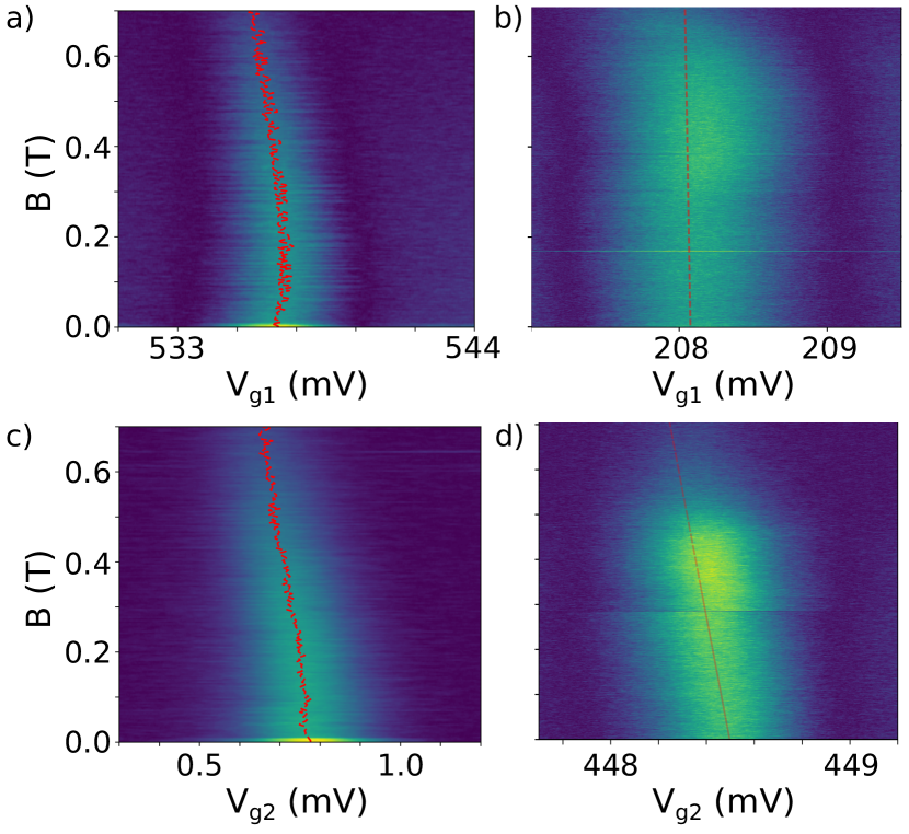
To determine the various lever-arms of our DQD system, we carried out magnetospectroscopy on DTR lines on QDs one and two while sweeping and accordingly (as shown in Fig 8). By assuming a factor of two, we are then able to extract the lever arms as follows
| (44) |
where is the Bohr magneton, is the change in the applied magnetic field and is the charge of an electron. The extracted lever arm matrix is
| (45) |
For the DTR simulations of QD 1, was used, while for the ICT .
Appendix G Electron temperature:
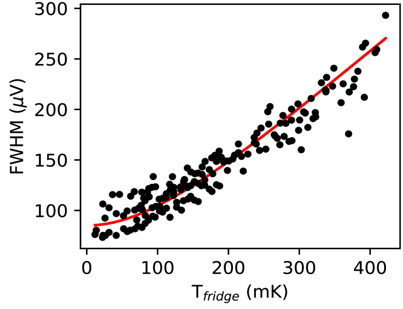
To set an upper bound for the electron temperature , we find the narrowest DTR (black line in Fig. 9) on QD one and measure its FWHM as a function of the mixing chamber fridge-temperature . We tune the device to a different region in voltage space, where the signal is narrower than the lifetime broadened DTR used for multiplication (see Fig. 9).
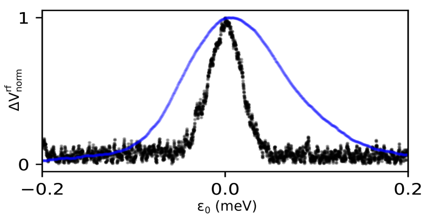
We ensured no power broadening by measuring the transition at varying rf powers [22]. From the temperature dependence measurements in Fig. 10, we fit the following expression to extract ,
| (46) |
From the fit, we estimate an upper bound for the electron temperature of 1403 mK.
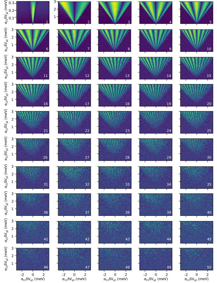
Appendix H DTR harmonics:
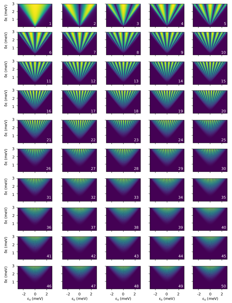
In this section, we present measurements and simulations of the DTR harmonics from to , see Fig. 11 and 12, respectively.
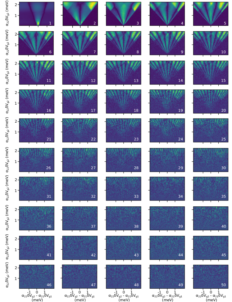
Appendix I ICT harmonics:
In this section, we present measurements and simulations of the ICT harmonics from to , see Fig. 13 and 14, respectively.
Appendix J Power conversion efficiency extraction:
The measurements in Appendices H and I were used to extract the power conversion efficiency for the DTR and ICT. The acquired data was limited to rf powers where no excited states or interference between multiple transitions were present (see Appendix K). The maximum signal would then occur at zero detuning for the odd harmonics, while for the even ones, it depends linearly on . For each harmonic, we have extracted the measured maximum signal at each rf power along with the corresponding fitted value, as shown in Fig. 15. These were then used to plot the power conversion relationship shown in Fig. 3a.
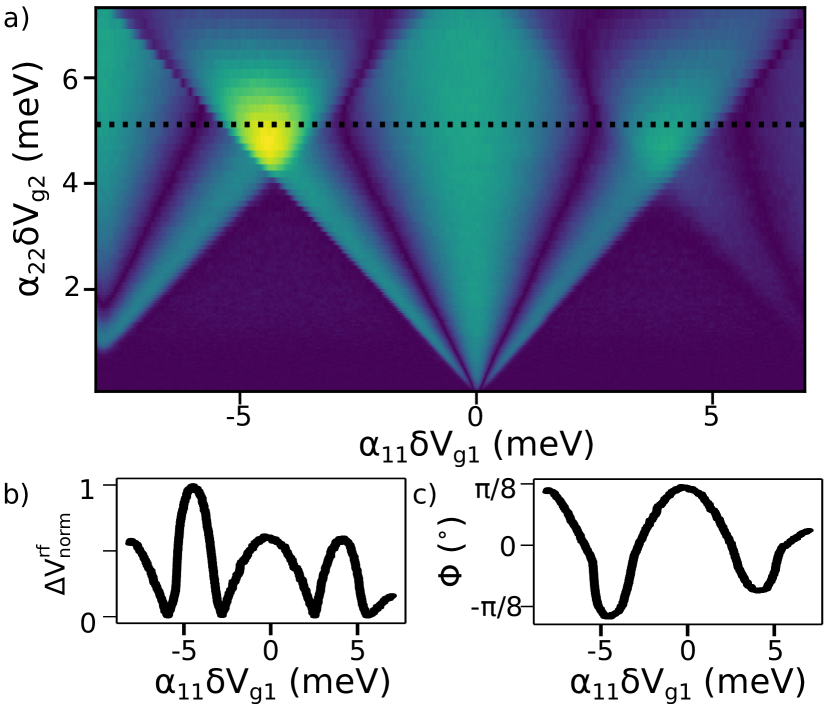
Appendix K Beyond N-2 dependence:
At high powers, it is possible to drive the system strongly to overcome the expected power conversion dependence of . In particular, for the ICT, an increment in signal is possible if excited states are present, as shown in Fig. 16a. This is due to a gain in quantum capacitance due to an increase in curvature of the eigenenergies. By driving the system even harder, it is possible to get multiple charges to transition, resulting in an interference pattern, as highlighted in Fig. 16b. We can thus find regions in voltage that should theoretically result in an increase of in power conversion that will counteract the expected relationship; this allowed us to measure a signal at even higher harmonics, such as , as shown in Fig. 16c.
Appendix L Ideal phase noise:
The phase noise of an rf source dominated by noise can be empirically described by Leeson’s equation [34]
| (47) |
where is the offset frequency from the carrier frequency , is an empirically fitted parameter known as the noise factor, is the power of the rf source, is the loaded quality factor, and is the corner frequency. The dependence arises from the decrease in voltage frequency response for an ideal tank circuit as a function of , which is then squared to convert it into power. The noise factor and the additive one within the first set of brackets account for the noise floor. The second parentheses provide the 1/ behaviour observed at limited offset frequencies.
An ideal frequency multiplier performs a rigid shift in the frequency axis, which, after multiplication, increases the phase noise by a factor of . For harmonics at the same frequency offset , as is the case in our data in Fig. 3, the ideal phase noise is:
| (48) |
References
- Loss and DiVincenzo [1998] D. Loss and D. P. DiVincenzo, Phys. Rev. A 57, 120 (1998).
- Hendrickx et al. [2021] N. W. Hendrickx, W. I. Lawrie, M. Russ, F. van Riggelen, S. L. de Snoo, R. N. Schouten, A. Sammak, G. Scappucci, and M. Veldhorst, Nature 591, 580 (2021).
- Philips et al. [2022] S. G. J. Philips, M. T. Ma̧dzik, S. V. Amitonov, S. L. de Snoo, M. Russ, N. Kalhor, C. Volk, W. I. L. Lawrie, D. Brousse, L. Tryputen, B. P. Wuetz, A. Sammak, M. Veldhorst, G. Scappucci, and L. M. K. Vandersypen, Nature 609, 919 (2022).
- Borsoi et al. [2022] F. Borsoi, N. W. Hendrickx, V. John, S. Motz, F. van Riggelen, A. Sammak, S. L. de Snoo, G. Scappucci, and M. Veldhorst, Shared control of a 16 semiconductor quantum dot crossbar array (2022).
- Xue et al. [2022] X. Xue, M. Russ, N. Samkharadze, B. Undseth, A. Sammak, G. Scappucci, and L. M. Vandersypen, Nature 601, 343 (2022).
- Noiri et al. [2022] A. Noiri, K. Takeda, T. Nakajima, T. Kobayashi, A. Sammak, G. Scappucci, and S. Tarucha, Nature 601, 338 (2022).
- Mills et al. [2022] A. R. Mills, C. R. Guinn, M. J. Gullans, A. J. Sigillito, M. M. Feldman, E. Nielsen, and J. R. Petta, Science Advances 8, eabn5130 (2022).
- Maurand et al. [2016] R. Maurand, X. Jehl, D. Kotekar-Patil, A. Corna, H. Bohuslavskyi, R. Laviéville, L. Hutin, S. Barraud, M. Vinet, M. Sanquer, and S. De Franceschi, Nat. Commun. 7, 13575 (2016).
- Zwerver et al. [2022] A. Zwerver, T. Krähenmann, T. Watson, L. Lampert, H. C. George, R. Pillarisetty, S. Bojarski, P. Amin, S. Amitonov, J. Boter, et al., Nature Electronics 5, 184 (2022).
- Charbon et al. [2016] E. Charbon, F. Sebastiano, A. Vladimirescu, H. Homulle, S. Visser, L. Song, and R. M. Incandela, in 2016 IEEE International Electron Devices Meeting (IEDM) (2016) pp. 13.5.1–13.5.4.
- Xue et al. [2021] X. Xue, B. Patra, J. P. van Dijk, N. Samkharadze, S. Subramanian, A. Corna, B. Paquelet Wuetz, C. Jeon, F. Sheikh, E. Juarez-Hernandez, et al., Nature 593, 205 (2021).
- Ruffino et al. [2022] A. Ruffino, T.-Y. Yang, J. Michniewicz, Y. Peng, E. Charbon, and M. F. Gonzalez-Zalba, Nature Electronics 5, 53 (2022).
- Li et al. [2018] R. Li, L. Petit, D. P. Franke, J. P. Dehollain, J. Helsen, M. Steudtner, N. K. Thomas, Z. R. Yoscovits, K. J. Singh, S. Wehner, et al., Science advances 4, eaar3960 (2018).
- Veldhorst et al. [2017] M. Veldhorst, H. Eenink, C.-H. Yang, and A. S. Dzurak, Nature communications 8, 1 (2017).
- Vandersypen et al. [2017] L. Vandersypen, H. Bluhm, J. Clarke, A. Dzurak, R. Ishihara, A. Morello, D. Reilly, L. Schreiber, and M. Veldhorst, npj Quantum Information 3, 1 (2017).
- Gonzalez-Zalba et al. [2021] M. Gonzalez-Zalba, S. de Franceschi, E. Charbon, T. Meunier, M. Vinet, and A. Dzurak, Nature Electronics 4, 872 (2021).
- Boter et al. [2022] J. M. Boter, J. P. Dehollain, J. P. Van Dijk, Y. Xu, T. Hensgens, R. Versluis, H. W. Naus, J. S. Clarke, M. Veldhorst, F. Sebastiano, et al., Phys. Rev. Appl. 18, 024053 (2022).
- Crawford et al. [2022] O. Crawford, J. Cruise, N. Mertig, and M. Gonzalez-Zalba, arXiv preprint arXiv:2201.02877 (2022).
- Fogarty [2022] M. A. Fogarty, arXiv preprint arXiv:2208.09172 (2022).
- Oakes et al. [2022] G. Oakes, V. Ciriano-Tejel, D. Wise, M. Fogarty, T. Lundberg, C. Lainé, S. Schaal, F. Martins, D. Ibberson, L. Hutin, et al., arXiv preprint arXiv:2203.06608 (2022).
- Niegemann et al. [2022] D. J. Niegemann, V. El-Homsy, B. Jadot, M. Nurizzo, B. Cardoso-Paz, E. Chanrion, M. Dartiailh, B. Klemt, V. Thiney, C. Bäuerle, P.-A. Mortemousque, B. Bertrand, H. Niebojewski, M. Vinet, F. Balestro, T. Meunier, and M. Urdampilleta, Parity and singlet-triplet high fidelity readout in a silicon double quantum dot at 0.5 k (2022).
- Ahmed et al. [2018] I. Ahmed, A. Chatterjee, S. Barraud, J. J. Morton, J. A. Haigh, and M. F. Gonzalez-Zalba, Commun. Phys. 1, 1 (2018).
- Chawner et al. [2021] J. Chawner, S. Barraud, M. Gonzalez-Zalba, S. Holt, E. Laird, Y. A. Pashkin, and J. Prance, Phys. Rev. Appl. 15, 034044 (2021).
- Cochrane et al. [2022a] L. Cochrane, T. Lundberg, D. J. Ibberson, L. A. Ibberson, L. Hutin, B. Bertrand, N. Stelmashenko, J. W. A. Robinson, M. Vinet, A. A. Seshia, and M. F. Gonzalez-Zalba, Phys. Rev. Lett. 128, 197701 (2022a).
- Nguyen [2007] C. T.-c. Nguyen, IEEE Transactions on Ultrasonics, Ferroelectrics, and Frequency Control 54, 251 (2007).
- Ibberson et al. [2018] D. J. Ibberson, L. Bourdet, J. C. Abadillo-Uriel, I. Ahmed, S. Barraud, M. J. Calderón, Y.-M. Niquet, and M. F. Gonzalez-Zalba, Applied Physics Letters 113, 53104 (2018).
- Pet [2010] Nano Lett. 10, 2789 (2010).
- Ciccarelli and Ferguson [2011] C. Ciccarelli and A. J. Ferguson, New Journal of Physics 13, 093015 (2011).
- Chorley et al. [2012] S. J. Chorley, J. Wabnig, Z. V. Penfold-Fitch, K. D. Petersson, J. Frake, C. G. Smith, and M. R. Buitelaar, Phys. Rev. Lett. 108, 036802 (2012).
- Mizuta et al. [2017] R. Mizuta, R. M. Otxoa, A. C. Betz, and M. F. Gonzalez-Zalba, Phys. Rev. B 95, 045414 (2017).
- Esterli et al. [2019] M. Esterli, R. Otxoa, and M. Gonzalez-Zalba, Applied Physics Letters 114, 10.1063/1.5098889 (2019).
- Derakhshan Maman et al. [2020] V. Derakhshan Maman, M. Gonzalez-Zalba, and A. Pályi, Phys. Rev. Appl. 14, 064024 (2020).
- Manzano [2020] D. Manzano, AIP Advances 10, 025106 (2020), publisher: American Institute of Physics.
- Lee and Hajimiri [2000] T. H. Lee and A. Hajimiri, IEEE journal of solid-state circuits 35, 326 (2000).
- Zhao et al. [2019] R. Zhao, T. Tanttu, K. Y. Tan, B. Hensen, K. W. Chan, J. C. C. Hwang, R. C. C. Leon, C. H. Yang, W. Gilbert, F. E. Hudson, K. M. Itoh, A. A. Kiselev, T. D. Ladd, A. Morello, A. Laucht, and A. S. Dzurak, Nat Commun 10, 5500 (2019).
- Veldhorst et al. [2014] M. Veldhorst, J. C. C. Hwang, C. H. Yang, A. W. Leenstra, B. de Ronde, J. P. Dehollain, J. T. Muhonen, F. E. Hudson, K. M. Itoh, A. Morello, and A. S. Dzurak, Nat Nanotech 9, 981 (2014).
- Vigneau et al. [2022] F. Vigneau, F. Fedele, A. Chatterjee, D. Reilly, F. Kuemmeth, F. Gonzalez-Zalba, E. Laird, and N. Ares, Probing quantum devices with radio-frequency reflectometry (2022).
- Colless et al. [2013] J. I. Colless, A. C. Mahoney, J. M. Hornibrook, A. C. Doherty, H. Lu, A. C. Gossard, and D. J. Reilly, Phys. Rev. Lett. 110, 046805 (2013).
- Gonzalez-Zalba et al. [2015] M. F. Gonzalez-Zalba, S. Barraud, A. J. Ferguson, and A. C. Betz, Nat Commun 6, 6084 (2015).
- Ares et al. [2016] N. Ares, F. J. Schupp, A. Mavalankar, G. Rogers, J. Griffiths, G. A. C. Jones, I. Farrer, D. A. Ritchie, C. G. Smith, A. Cottet, G. A. D. Briggs, and E. A. Laird, Phys. Rev. Appl. 5, 034011 (2016).
- Shevchenko et al. [2010] S. Shevchenko, S. Ashhab, and F. Nori, Phy Rep 492, 1 (2010).
- Cochrane et al. [2022b] L. Cochrane, A. A. Seshia, and M. F. G. Zalba, Intrinsic noise of the single electron box (2022b).