1 Hardware Design and Implementation
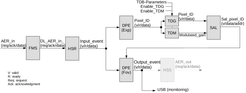
Fig. 1 shows a schematic of the proposed architecture, which consists of seven blocks. The Handshake Receiver (HSR) handles the input events. HSR implements the standard 4-phase handshake AER protocol between the sender and the receiver block. The output events are monitored through a USB connection but can also be sent to the other event-based devices using a Handshake Sender (faded HSS block in Fig. 1). To prevent meta-stable states at the interface between different clock domains, a double flip-flop synchronizer (FMS) is applied before the input handshake. The core blocks of the architecture are described in more detail in the following sections.
1.1 Data Processing Element(DPE)
The event-camera included in our architecture is the DAVIS240C which employs a serial data format, i.e. x and y coordinates of the events are sent one after the other [DVS, Brandli_etal14]. Thus, the Data Processing Element block (or DPE) takes care of generating the 2D event coordinate by merging x and y input words and forwards the resulting pixel_ID to the receiver block. Two instances of this block are used, which differ in the spatial resolution of the output events.
-
•
DPE Exploring, or DPE (Exp), which operates on the full input resolution, extracts the pixel_ID from the input events and forwards it to the Saliency block (SAL); SAL defines the most salient pixel according to the input events and a history of the previous events.
-
•
DPE Fovea, or DPE (Fov), which receives the coordinate of the most salient pixel by the SAL block and extracts only the events inside the FOA.
1.2 Top-Down Biasing Blocks
After exploring the input events and extracting the pixel_ID, the top-down mechanism works on top of the bottom-up saliency. In the proposed system, the top-down biasing mechanism is implemented using two different methods. Both are explained in more detail in LABEL:method_tdb.
1.2.1 Top-Down Gating (TDG)
This block receives the extracted pixel_ID from DPE (Exp) block. When this block is enabled, via the input parameter Enable_TDG, input events cross the TDG only if they meet the input top-down biasing conditions (TDB_parameters).
1.2.2 Top-Down Modulation (TDM)
TDM also receives the pixel_IDs from the DPE (Exp). This block handles all the input events with a modulated state-changing gain. The amplitude of the modulation depends on the top-down biasing conditions. The highest modulation happens when the input events meet the TDM requirements.
1.3 Saliency block (SAL)
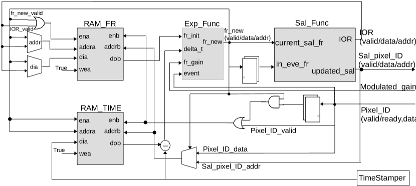
Fig. 2 illustrates the core blocks of the Saliency Block (or SAL) architecture. SAL extracts the location of the most salient pixel. In the SAL architecture two separate Dual Port BRAM are used: RAM_FR stores the pixel state as 21-bits registers (with fixed-point representation: s=1 bit for the sign, i=12 integer bits, and f=8 fractional bits); RAM_TIME stores timestamp of the last event generated at each pixel location.
Let be the current most salient pixel location with state , which is selected based on all the previous input events. At each incoming event from pixel at time point , the SAL block performs the following steps:
-
1.
Read the last pixel event time stamp from the corresponding entry of the RAM_TIME.
-
2.
Read the latest pixel state at the last pixel event timestamp from the corresponding entry of the RAM_FR.
-
3.
Compute the updated pixel state as follows:
(1) with stored as input parameter. This operation is handled by Exp_Func block (Fig. 2), where the exponential decay term is implemented using the piece-wise linear approximation, to reduce the hardware resource utilization on the FPGA.
-
4.
Store the new pixel state and timestamp in the corresponding BRAM entries.
-
5.
Update the state of the current most salient pixel by repeating steps 1, 2, and 3 for .
-
6.
Compare the new pixel state to the state of the current most salient pixel . If :
-
•
Update the most salient pixel location, which is forwarded to the DPE(Fov) block.
-
•
Excite the state of the updated most salient pixel as the center of FOV or :
(2) -
•
Inhibit the state of all pixels in the previous FOA:
(3) with and stored as input parameters for the highest excitation and inhibition values, respectively.
By penalizing the pixels in the previously selected salient region, the last step adapts the Inhibition of Return (IOR) mechanism proposed in [Itti_Koch01] to our event-based implementation.
-
•