figure \cftpagenumbersofftable
Robust moiré flatbands within a broad band-offset range
Abstract
Photonic analogs of the moiré superlattices mediated by interlayer electromagnetic coupling are expected to give rise to rich phenomena such as nontrivial flatband topology. Here, we propose and demonstrate a scheme to tune the flatbands in a bilayer moiré superlattice by employing the band offset. The band offset is changed by fixing the bands of one slab while shifting those of the other slab, which is accomplished by modifying the thickness of the latter slab. Our results show that the band-offset tuning not only makes some flatbands emerge and disappear, but also leads to two sets of flatbands that are robustly formed even with the change of band offset over a broad range. These robust flatbands form either at the AA-stack site or at the AB-stack site, and as a result, a single-cell superlattice can support a pair of high-quality localized modes with tunable frequencies. Moreover, we develop a diagrammatic model to provide an intuitive insight into the formation of the robust flatbands. Our work demonstrates a simple yet efficient way to design and control complex moiré flatbands, providing new opportunities to utilize photonic moiré superlattices for advanced light-matter interaction including lasing and nonlinear harmonic generation.
keywords:
moiré superlattice, robust flatbands, doubly-resonant superlattice, diagrammatic model*\linkableplhong@uestc.edu.cn +\linkableliangyi@gxu.edu.cn
1 Introduction
Moiré physics is a nascent yet exciting research direction that has led to important discoveries in various areas, ranging from electronics, to optics, and to acoustics [1, 2, 3, 4]. Moiré physics is associated with the emergence of novel phases that are not present in the individual lattices of the superlattice, leading to intriguing physical phenomena. For instance, when two monolayer materials are brought into contact, the moiré potentials have been predicted and demonstrated to strongly modify the optical properties of the bilayer materials [5, 6, 7, 8, 9]. Indeed, the initial breakthrough was made in condensed matter systems by discovering exotic phenomena in moiré superlattices, including unconventional superconductivity [10], moiré excitons [6, 7, 8, 9], anomalous Hall ferromagnetism [11], to name just a few. These novel moiré effects are discovered in superlattices with appropriate interlayer coupling, but the realization of the nontrivial superlattice needs fine tuning of the 2d materials, as initiated by the seminal work on twisted bilayer graphene [10, 12]. The difficulty arises from the reliance of the moiré effects on the formation of flatbands that only occur at magic angles in the superlattices [10, 12, 13]. Later, the concept of moiré physics was introduced into the realm of optics, where flexible control on superlattices is feasible [2, 4]. The tunability of photonic superlattices is particularly beneficial for exploring flatband physics and relevant photonic applications.
In photonics, several research groups have studied intriguing moiré physics with mismatched photonic lattices [14, 15], and twisted bilayer photonic slabs [16, 17, 18, 19, 20]. The moiré bands are typically tuned either by twisting the bilayer slabs or by modifying the optical distance between the two slabs. Especially, the flatbands relevant to novel moiré physics are found at photonic magic angles [16, 20], demonstrating a striking similarity with the electronic twisted bilayer graphene. Besides, a flatband can also emerge by setting the optical distance to specific values, as discovered in the 2D twisted superlattices [16, 19] and 1D mismatched superlattices [15]. The appearance of flatbands underlies various optical phenomena such as topological transition of optical dispersion contours [17], non-Anderson-type localization of light [21], twisting-induced optical solitons [22], and moiré quasi-bound states in the continuum [23]. Obviously, flatbands play an essential role in exploring novel physics in optics. Besides, a flatband mode is typically localized [24, 25], making it highly valuable for manipulating light-matter interaction such as lasing [26] and optical harmonic generation [27]. Therefore, flatband formation lies at the heart of intriguing moiré physics and relevant applications. It is desirable and critical to develop efficient strategies to tune the moiré flatbands.
In this work, we employ the band offset in the band domain as an efficient knob to tune the flatbands in a mismatched bilayer superlattice. The band offset is changed by fixing the bands of one slab while shifting those of the other slab, which are realizable by modifying the thickness of the latter slab in practice. Remarkably, the band offset not only triggers the appearance and disappearance of a few flatbands, but also leads to two sets of flatbands that can robustly form within a broad band-offset range. By taking advantage of the robustly formed flatbands, we further demonstrate a doubly-resonant single-cell superlattice with localized modes originating from the flatbands, and the frequencies of these modes are tunable by band offset. Such localized modes hold great promise for manipulating advanced light-matter interaction. Moreover, we develop a diagrammatic model to provide an intuitive insight into the formation of these robust flatbands, which can inspire new design approaches for moiré superlattices with tailored flatbands. Our work thus provides an efficient way to understand and control the formation of flatbands. Since the robust flatbands can be achieved without requiring strict magic configuration, they may have great potential in relevant applications based on moiré devices.
2 Results
2.1 Scheme and adjustable band offset
Our superlattice is constructed by stacking two mismatched silicon slabs in a commensurate configuration shown in Figure 1(a). The unit size of slab 1 is , while that of slab 2 is . Here, is an integer (fixed to be 13 hereafter), and = 300 nm. The resulting moiré superlattice has a unit size . Certainly, one can choose other values of , and changes accordingly. The width of the silicon strip is fixed to be . In the superlattice, slab-1’s silicon strip can align with slab-2’s silicon strip, creating the AA-stack site, indicated as “A” in Figure 1(a). Slab-1’ silicon strip can also align with the slab-2’s air gap, creating the AB-stack site, indicated as “B” in Figure 1(a).
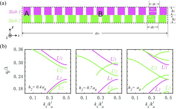
To exploit the band offset as a degree of freedom to tune the moiré bands in the superlattice, we keep the thickness () of slab 1 fixed at 0.4, but change the thickness () of slab 2 from 0.4 to . As a result, the bands of slab 1 remain unchanged, while the spectral positions of slab-2’s bands are shifted. Hence, the band offset between the two slabs is modified. Hereafter, we focus on the TE bands, of which the electric field is polarized along axis. The TE bands at different conditions are obtained by solving the wave equation
| (1) |
Here, is the frequency, is the velocity of light in the vacuum, and is the relative permittivity. The refractive indices of the silicon and the air are set to be 3.47 and 1, respectively. In this work, the wave equation is numerically solved through finite-element computation with Comsol Multiphysics. Notably, some bands of the photonic slabs are above the light line , and therefore light can leak into the free space surrounding the slabs. Consequently, the eigenfrequency is typically a complex value , and the quality factor describes how well an eigenmode is confined in the slabs.
Figure 1(b) shows the TE bands of the two slabs at different (). For clarity, we only draw the eigenmodes with quality factors , and therefore some bands look incomplete in the figure. Within the spectral range of interest, slab 1 has two lowest bands ( and ) that remain unchanged in the band domain. Slab 2 also has two lowest bands ( and ) at , and an initial band offset between and ( and ) can be seen. When increases to , and move downward, while intersects with another band. As increases to , and move downward further. Clearly, the band offset between and ( and ) increases with the increase of the thickness . Thus, the band offset is adjusted efficiently by scanning the thickness of slab 2.
2.2 Robust flatbands
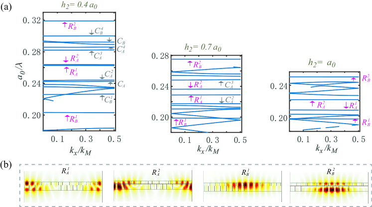
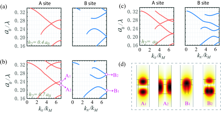
Next, we investigate how the moiré bands are tuned by the band offset. The moiré bands of the superlattice (with and ) are shown in Figure 2(a). The cell length of the superlattice is much larger, i.e. times of that of slab 2. As a result, while a band of slab 2 can extend over in the -space, the superlattice has mini-bands that only extend over of in the k-space. We have identified the flatbands that have a frequency deviation meeting the condition . For clarity, the flatbands with similar field patterns are marked by a same symbol. The results show that multiple flatbands emerge at each band offset, but some flatbands may disappear when the band offset changes. Specifically, the flatbands and emerge at , but disappear at and . The flatband has a frequency deviation of 0.08% at and a smaller frequency deviation of 0.02% at , but disappears at . The flatband has a frequency deviation of 0.05% and a larger frequency deviation of 0.12% at , but disappears at . Such emerging and disappearing flatbands demonstrate the important role of band offset in tuning the flatbands.
Remarkably, there are four flatbands that can form robustly at different band offsets through the entire scan range, labeled as and in Figure 2(a) for clarity. The field patterns of these robust flatbands are shown in Figure 2(b). It is seen that the and modes are strongly localized around A site of the superlattice, while the and modes are strongly localized around B site of the superlattice. The stable formation of the flatbands is quite desirable in practice, because they can be achieved without the need for a subtle magic configuration.
2.3 Doubly-resonant single-cell superlattice
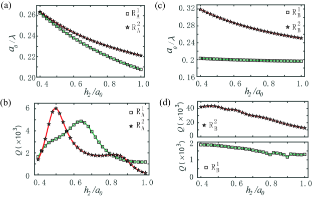
The simultaneous emergence of multiple robust flatbands paves the way toward multiply-resonant superlattice with tunable frequencies, since scanning the band offset does not make these flatbands disappear but rather allows us to control their spectral positions. Particularly, these robust flatbands can even be supported by only a single-cell superlattice, due to their strongly localized wavefunctions. We thus calculate the eigenfrequencies of localized modes with a single-cell superlattice, and focus on those originating from the robust flatbands. The and modes are studied with an A-site centered single-cell superlattice, while and modes are studied with a B-site centered single-cell superlattice. The spectral positions of and modes at different are shown in Figure 3(a), and those for and modes are shown in Figure 3(c). The and modes are nearly degenerate at 0.4, and gradually separate when increases. In contrast, and modes start at a large spectral separation, and become closer in spectrum when increases. Notably, the frequency of mode keeps almost invariant against the change of .
Besides, we calculated the quality factor of these flatband modes at different . The quality factor of mode is peaked at with a value , but keeps larger than 1000 within the entire range as shown in Figure 3(b). The quality factor of mode is peaked near with a value , but keeps larger than 1000 up to . For and modes shown in Figure 3(d), the quality factor of mode decreases slightly from 2000 to 1300 within the scan range, while the quality factor of mode keeps a high value that is between 12000 and 43000. These results show that the robust-flatband resonances hold high quality even in a single-cell superlattice, demonstrating the possibility of constructing a high-quality multiply-resonant superlattice.
2.4 A diagrammatic model
Next, we provide an intuitive insight into the formation of the robust flatbands by employing a simplified two-site coupled-band diagram. Our model originates from the realization that the local dielectric structure continuously changes from A site to B site in the superlattice, i.e. other local positions in the superlattice have effective dielectric structures belonging to the intermediate states between A site and B site. Consequently, we consider a two-site diagram that only consists of two sets of bands related to A site and B site. Specifically, one set of bands corresponds to a fictitious lattice with an A-site-like unit cell, and the other set of bands corresponds to a fictitious lattice with B-site-like unit cell. The bands of the fictitious lattices originate from the interlayer coupling between the two slabs. Under a two-mode coupling approximation, the eigenfrequencies of coupled eigenmodes are given by [28]
| (2) |
Here denotes the frequency of the eigenmode of slab such as / schematically shown in Figure 4(a), and denotes the frequencies of the coupled eigenmodes. Generally, a strong interlayer coupling coefficient leads to a larger spectral gap between the pair of coupled eigenmodes compared to . The interlayer coupling coefficient is determined by the overlap of the field patterns that correspond to the pair of eigenmodes [29]. Specifically, has a spot-like field pattern with its maxima at the silicon strip, while has a spot-like field pattern with its maxima at the air gap. At the A site, the field maxima of () align with that of (), such that their coupling coefficient is large. The strong coupling increases the spectral gap between and ( and ), forming a coupled band diagram schematically shown in Figure 4(b). At the B site, the field maxima of align with that of , and thus their coupling coefficient is large. The strong coupling increases the spectral gap between and , leading to a bandgap structure schematically shown in Figure 4(c). The two sets of coupled bands in Figure 4(b) and 4(c) constitute our two-site coupled-band diagram.
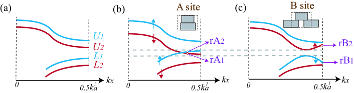
In this simplified two-site band diagram, two bands ( and ) at A site always locate within the bandgap at B site. This unique band structure gives rise to optical modes that are hosted at A site but do not extend to B site. Consequently, a pair of robust flatbands always form at A site, as long as the coupled-band gap structure does not change. This explains the robust formation of the flatbands and at A site in the superlattice. On the other hand, the pair of coupled bands at B site ( and ) reach extrema at the band edges, which are related to the robust flatbands and . Although the coupled-band edges do not locate within a bandgap at A site, they are in resonance with only one band point at A site. Moreover, the strong band coupling makes the spatial patterns of coupled eigenmodes at B site poorly overlap with those of the resonant eigenmodes at A site. As a result, the leakage to A site is weak, leading to the formation of and localized at B site. The flatbands and are stable as long as the coupled-band structure persists. Thus, the simple two-site band diagram gives us an intuitive understanding of the formation of the robust flatbands.
To further confirm the diagrammatic model, we implement full-wave calculation to obtain the accurate coupled bands of the A-site and B-site like fictitious lattices, separately. Figures 5(a)-5(c) show the two-site coupled bands at different (= and ). The crossing bands at A site, as well as the band gap at B site, are clearly seen in the results. Moreover, we draw the field patterns of the four modes marked by , , and in Figure 5(b), as seen in Figure 5(d). These field patterns are in a good agreement with the field patterns of the robust flatbands at A site ( and ) and B site ( and ) shown in Figure 2(b). This agreement adequately confirms our theoretical explanation on the formation of the robust flatbands.
3 Discussion
The robust flatbands differ significantly from those that are sensitive to the change of band offset, indicating the complex formation process of moiré flatbands. The proposed diagrammatic model provides an intuitive understanding on the formation of robust flatbands with regard to the band offset. Notably, the situation in twisted superlattices is much more complicated than the global band offset simply used in our work. When the twist angle is adjusted, locally variable band offsets are introduced in the parameter space, together with twist-dependent dielectric structures in the real space. Nonetheless, our results may provide a straightforward approach for comprehending the formation of relatively stable flatbands in twisted superlattices [30, 31].
Besides, the diagrammatic model can guide new designs of moiré superlattices. For instance, one can intentionally design two unit cells, and let them form a two-site band diagram similar to that shown in Figures 4(b) and 4(c). The two unit cells can be bilayer ones, as well as multi-layer ones or even monolayer ones. Then, a moiré superlattice can be constructed by connecting the two unit cells with intermediate-state cells, of which the formation of robust flatbands can be predicted under the two-site band diagram. The field patterns of the robust flatbands can also be estimated by referring to the eigenmodes of the pair of unit cells. Clearly, our two-site diagrammatic model significantly simplifies the design of moiré superlattices with tailored flatbands.
Furthermore, due to the robust formation of these flatband modes, it is possible to achieve dynamic control of their frequencies in practice. For instance, one can fabricate a lattice with multiple domains, and each domain has a different thickness. By shifting the multiple-domain lattice with regard to another finite-size lattice of fixed thickness, the flatband modes stably form in the bilayer region, but alter their frequencies. Therefore, the band-offset tuning has great potential for enhancing functionalities of moiré photonic devices. Certainly, structural perturbations in the superlattice could affect the flatbands, with the extent of this influence dependent on the specific fabrication conditions. Further studies are necessary to explore and understand these effects, which may be useful for experimental implementations, especially as several experimental techniques have demonstrated their capability of realizing nontrivial moiré superlattices, including nanofabrication [26], photorefractive effect [22, 21], and femtosecond-laser writing [32].
4 Conclusion
In conclusion, we have demonstrated that the band offset can be an efficient knob to tune the flatbands in a moiré superlattice. The band offset not only makes a few flatbands emerge and disappear, but also leads to multiple robust flatbands with their wavefunctions localized at different stacking sites. These robust flatbands offer promising avenues for constructing multiply-resonant moiré superlattices with tunable frequencies, as illustrated by the analysis of a single-cell superlattice. Moreover, we have developed a diagrammatic model that provides an intuitive insight into the formation mechanism of the two sets of robust flatbands, which can inspire new designs of moiré superlattices. Our scheme may be further developed with AI-empowered techniques, which may prove relevant to next-generation device designs for nanophotonics [33]. In particular, this work represents an important step toward controlling and understanding complex flatbands in moiré superlattices, and may bring about new opportunities for exploiting moiré superlattices in manipulating advanced light-matter interactions such as lasing [26], nonlinear harmonic generation [27], and enhanced free-electron radiation [34].
Disclosures
The authors declare no conflict of interest.
Acknowledgments
This work was supported by Sichuan Science and Technology Program (2023NSFSC0460), the Fundamental Research Funds for the Central Universities (ZYGX2020J010), the Open Project Funding of the Ministry of Education Key Laboratory of Weak-Light Nonlinear Photonics (OS22-1), Guangxi Natural Science Foundation (2020GXNSFAA297041), the National Key R&D Program of China (2022YFA1404800), and the National Natural Science Foundation (12134006).
Data Availability
The data that support the findings of this article are not publicly available. They can be requested from the corresponding authors upon reasonable request.
References
- [1] E. Y. Andrei, D. K. Efetov, P. Jarillo-Herrero, et al., “The marvels of moiré materials,” Nat. Rev. Mater. 6(3), 201–206 (2021).
- [2] J. Chen, X. Lin, M. Chen, et al., “A perspective of twisted photonic structures,” Appl. Phys. Lett. 119(24), 240501 (2021).
- [3] Y. Deng, M. Oudich, N. J. Gerard, et al., “Magic-angle bilayer phononic graphene,” Phys. Rev. B 102(18), 180304(R) (2020).
- [4] L. Du, M. R. Molas, Z. Huang, et al., “Moiré photonics and optoelectronics,” Science 379(6639), eadg0014 (2023).
- [5] B. Urbaszek and A. Srivastava, “Materials in flatland twist and shine,” Nature 567, 30–40 (2019).
- [6] K. Tran, G. Moody, F. Wu, et al., “Evidence for moiré excitons in van der waals heterostructures,” Nature 567(7746), 71–75 (2019).
- [7] K. L. Seyler, P. Rivera, H. Yu, et al., “Signatures of moiré-trapped valley excitons in mose2/wse2 heterobilayers,” Nature 567(7746), 66–70 (2019).
- [8] E. M. Alexeev, D. A. Ruiz-Tijerina, M. Danovich, et al., “Resonantly hybridized excitons in moiré superlattices in van der waals heterostructures,” Nature 567(7746), 81–86 (2019).
- [9] C. Jin, E. C. Regan, A. Yan, et al., “Observation of moiré excitons in wse2/ws2 heterostructure superlattices,” Nature 567(7746), 76–80 (2019).
- [10] Y. Cao, V. Fatemi, S. Fang, et al., “Unconventional superconductivity in magic-angle graphene superlattices,” Nature 556(7699), 43–50 (2018).
- [11] N. Bultinck, S. Chatterjee, and M. P. Zaletel, “Mechanism for anomalous hall ferromagnetism in twisted bilayer graphene,” Phys. Rev. Lett. 124(16), 166601 (2020).
- [12] Y. Cao, V. Fatemi, A. Demir, et al., “Correlated insulator behaviour at half-filling in magic-angle graphene superlattices,” Nature 556(7699), 80–84 (2018).
- [13] R. Bistritzer and A. H. MacDonald, “Moiré bands in twisted double-layer graphene,” Proc. Natl. Acad. Sci. U. S. A. 108(30), 12233–12237 (2011).
- [14] W. Wang, W. Gao, X. Chen, et al., “Moiré fringe induced gauge field in photonics,” Phys. Rev. Lett. 125(20), 203901 (2020).
- [15] D. X. Nguyen, X. Letartre, E. Drouard, et al., “Magic configurations in moiré superlattice of bilayer photonic crystals: Almost-perfect flatbands and unconventional localization,” Phys. Rev. Res. 4(3), L032031 (2022).
- [16] K. Dong, T. Zhang, J. Li, et al., “Flat bands in magic-angle bilayer photonic crystals at small twists.,” Phys. Rev. Lett. 126(22), 223601 (2021).
- [17] G. Hu, Q. Ou, G. Si, et al., “Topological polaritons and photonic magic angles in twisted -moo3 bilayers,” Nature 582(7811), 209–213 (2020).
- [18] B. Lou, N. Zhao, M. Minkov, et al., “Theory for twisted bilayer photonic crystal slabs,” Phys. Rev. Lett. 126(13), 136101 (2021).
- [19] M. Oudich, G. Su, Y. Deng, et al., “Photonic analog of bilayer graphene,” Phys. Rev. B 103(21), 214311 (2021).
- [20] H. Tang, F. Du, S. Carr, et al., “Modeling the optical properties of twisted bilayer photonic crystals,” Light Sci. Appl. 10(1), 1–8 (2021).
- [21] P. Wang, Y. Zheng, X. Chen, et al., “Localization and delocalization of light in photonic moiré lattices,” Nature 577(7788), 42–46 (2020).
- [22] Q. Fu, P. Wang, C. Huang, et al., “Optical soliton formation controlled by angle twisting in photonic moiré lattices,” Nat. Photonics 14(11), 663–668 (2020).
- [23] L. Huang, W. Zhang, and X. Zhang, “Moiré quasibound states in the continuum,” Phys. Rev. Lett. 128(25), 253901 (2022).
- [24] D. Leykam, A. Andreanov, and S. Flach, “Artificial flat band systems: from lattice models to experiments,” Adv. Phys.: X 3(1), 1473052 (2018).
- [25] L. Tang, D. Song, S. Xia, et al., “Photonic flat-band lattices and unconventional light localization,” Nanophotonics 9(5), 1161–1176 (2020).
- [26] X.-R. Mao, Z.-K. Shao, H.-Y. Luan, et al., “Magic-angle lasers in nanostructured moiré superlattice,” Nat. Nanotechnol. 16(10), 1099–1105 (2021).
- [27] P. Hong, L. Xu, C. Ying, et al., “Flatband mode in photonic moiré superlattice for boosting second-harmonic generation with monolayer van der waals crystals,” Opt. Lett. 47(9), 2326–2329 (2022).
- [28] M.-A. Miri and A. Alù, “Exceptional points in optics and photonics,” Science 363(6422), eaar7709 (2019).
- [29] H. A. Haus and W. Huang, “Coupled-mode theory,” Proc. IEEE 79(10), 1505–1518 (1991).
- [30] H. Wang, S. Ma, S. Zhang, et al., “Intrinsic superflat bands in general twisted bilayer systems,” Light Sci. Appl. 11(1), 159 (2022).
- [31] C.-H. Yi, H. C. Park, and M. J. Park, “Strong interlayer coupling and stable topological flat bands in twisted bilayer photonic moiré superlattices,” Light Sci. Appl. 11(1), 289 (2022).
- [32] A. Arkhipova, Y. Kartashov, S. Ivanov, et al., “Observation of linear and nonlinear light localization at the edges of moiré lattices,” Phys. Rev. Lett. 130(8), 083801 (2023).
- [33] Z. Chen and M. Segev, “Highlighting photonics: looking into the next decade,” eLight 1(1), 2 (2021).
- [34] Y. Yang, C. Roques-Carmes, S. E. Kooi, et al., “Photonic flatband resonances for free-electron radiation,” Nature 613(7942), 42–47 (2023).
Biographies and photographs of the authors are not available now.