HexaMesh: Scaling to Hundreds of Chiplets
with an Optimized Chiplet Arrangement
Abstract
2.5D integration is an important technique to tackle the growing cost of manufacturing chips in advanced technology nodes. This poses the challenge of providing high-performance inter-chiplet interconnects (ICIs). As the number of chiplets grows to tens or hundreds, it becomes infeasible to hand-optimize their arrangement in a way that maximizes the ICI performance. In this paper, we propose HexaMesh, an arrangement of chiplets that outperforms a grid arrangement both in theory (network diameter reduced by ; bisection bandwidth improved by ) and in practice (latency reduced by ; throughput improved by ). HexaMesh enables large-scale chiplet designs with high-performance ICIs.
I Introduction
CMOS technology scaling enables us to build chips with an ever-increasing transistor density. The main advantage of transitioning to a more advanced technology node is that it allows us to pack more transistors and hence more performance into chips of the same size. The downside of this transition is the increased complexity of the physical design, verification, firmware, and mask sets. As a result, the non-recurring cost almost doubles whenever we transition to a more advanced technology node [design-cost-exp]. Another challenge of manufacturing chips in advanced technology nodes is the high defect rate which diminishes the yield and increases the recurring cost. Due to these trends, making the design and fabrication of chips in bleeding-edge technology nodes economically viable has become a real challenge.
A promising solution to this challenge is the disaggregation of monolithic chips into multi-chip modules (MCMs). Current trends show that the only chips that keep up with Moore’s law [mooreslaw] are MCMs [lookingglass2022]. One strategy to create multi-chip modules is 2.5D integration in which the chip is disaggregated into multiple chiplets which are connected through an organic packaging substrate or silicon interposer. 2.5D integration has various economical advantages:
-
•
Heterogeneity: Different chiplets can be implemented in different technology nodes. Here, subcircuits that cannot take advantage of transistor scaling, e.g., I/O drivers, are fabricated in more mature technology nodes with lower non-recurring cost and higher yield.
-
•
Reuse: A given chiplet can be used in multiple designs. For example, we do not need to redesign the aforementioned I/O chiplet when the rest of the chip is transitioned to a more advanced technology node. As demonstrated by AMD [amd-chiplets], we can use the same compute-chiplet in multiple products with varying core-counts. Reuse avoids redesigning components, further reducing the non-recurring cost.
-
•
Improved Yield: A single fabrication defect can render a whole die useless, whether it is a chiplet or a monolithic chip. Since chiplets are smaller than monolithic chips, 2.5D integration reduces the area loss due to fabrication defects, hence improving the yield.
-
•
Binning: Power- and frequency-binning are important strategies to deal with parametric variation. In binning, chips are grouped into different bins (e.g., based on power consumption or maximum clock frequency) which are then priced differently. In 2.5D integration, binning is done on a per-chiplet scale, increasing the total revenue.
While 2.5D integration has many economical benefits, it also comes with technological challenges. One such challenge is the fact that a die-to-die (D2D) link requires a physical layer (PHY) interface in both the sending and the receiving chiplet. As a consequence, the total silicon area and power consumption of all chiplets combined exceed the area and power of a monolithic chip with the same functionality. However, the additional cost due to the PHY’s area and power overhead is often compensated by the other economical benefits of 2.5D integration. A more important challenge is creating a high-bandwidth and low-latency inter-chiplet interconnect (ICI). To connect chiplets to the package substrate, controlled collapse chip connection (C4) bumps are used and to connect them to a silicon interposer, one uses micro-bumps. The minimum pitch of these bumps limits the number of bumps per mm2 of chiplet area which limits the number and bandwidth of D2D links. As a consequence, D2D links are the bottleneck of the ICI.
Since the D2D links limit the ICI data width, we want to operate them at the highest frequency possible to maximize their throughput. To run such links at high frequencies without introducing unacceptable bit error rates, we must limit their length to a minimum [bow, ucie]. The length of D2D links is minimized if we only connect adjacent chiplets. However, with such restricted connections, the shape and arrangement of chiplets has a significant impact on the performance of the ICI.
In this paper, we analyze how to shape and arrange chiplets to maximize the ICI performance. We make the following contributions:
-
•
Problem Statement: We formulate a detailed problem statement including economics- and technology-driven constraints for the shape of chiplets and proxies for the ICI performance (Section III).
-
•
HexaMesh: We address the above problem by proposing the HexaMesh arrangement. HexaMesh asymptotically reduces the network diameter by and improves the bisection bandwidth by compared to a grid arrangement (Section IV).
-
•
D2D link model: Instead of only relying on network diameter and bisection bandwidth as performance proxies, we want to consider implementation details of the ICI. To do so, we introduce our model to estimate the bandwidth of D2D links (Section V).
-
•
Evaluation: We combine link bandwidth estimates using our model and cycle-level simulations using BookSim2 [booksim] to compare HexaMesh to a 2D grid. On average, HexaMesh reduces the latency by and improves the throughput by (Section VI).
II Background on 2.5D Integration
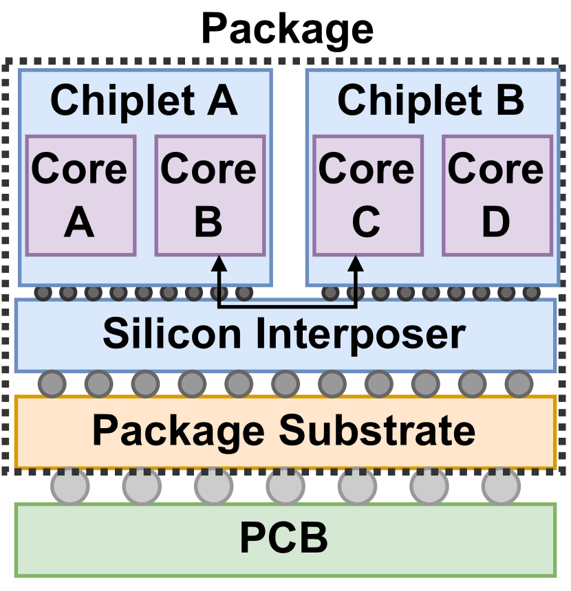
In 2.5D integration, multiple chiplets are enclosed in a single package. The two most prominent techniques to provide connectivity between chiplets are organic package substrates (see Figure 1(b)) and silicon interposers (see Figure 1(c)). Besides these established 2.5D integration schemes, there are more complex techniques, e.g., active interposers [intact]. Active interposers do not only contain wires but also transistors which allows constructing buffered wires or offloading some power management circuits from the chiplets to the interposer. However, active interposers come with additional challenges, e.g., reduced yield or thermal problems. In this work, we focus on passive silicon interposers and package substrates as they are more established.

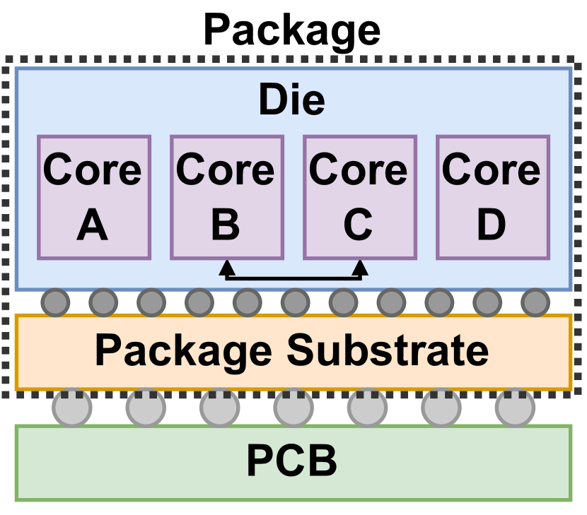
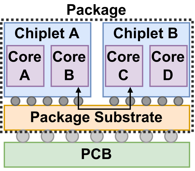
The organic package substrate provides connectivity between different chiplets and between chiplets and the printed circuit board (PCB). C4 bumps with a pitch of -m are used to connect chiplets to the package substrate. Connections between the package substrate and the PCB are built using solder bumps with a pitch of -m. The small pitch of C4 bumps enables the construction of D2D links that offer up to more bandwidth than off-chip links. This shows that the bandwidth between multiple chiplets in a 2.5D stacked chip is substantially higher than the bandwidth between multiple single-chip packages (SCPs) on the same PCB.
A silicon interposer can be added between the chiplets and the package substrate. Micro-bumps with a pitch of -m are used to connect chiplets to the interposer. Regular C4 bumps with a pitch of -m are used to connect the interposer to the package substrate. The reduced pitch of micro-bumps further enhances the throughput of D2D links. Besides increased design and manufacturing cost, silicon interposers also come with higher signal loss compared to package substrates [usr-links]. As a consequence, D2D links in silicon interposers need to be even shorter (mm [ucie]) to provide low bit error rates when operated at high frequencies.
D2D links often use different protocols, voltage levels, and clock frequencies than the intra-chiplet interconnect. The conversion between protocols, voltage levels, and clock frequencies is performed by a PHY which is added at the start and end of each D2D link. PHY s reside inside the chiplets and they introduce a certain area and power overhead compared to monolithic chips that do not require them. PHY s and ICI protocols have been standardized [bow, ucie] to achieve interoperability between chiplets from different manufacturers.
III The Problem of Chiplet Shape & Arrangement
In this section, we formalize the problem of finding chiplet shapes and arrangements. To do so, we define technology- and economics-driven constraints for the shape of chiplets. We also introduce proxies for the performance of the ICI be able to assess a given arrangement without making any assumptions on implementation details.
III-A Assumptions and Scope
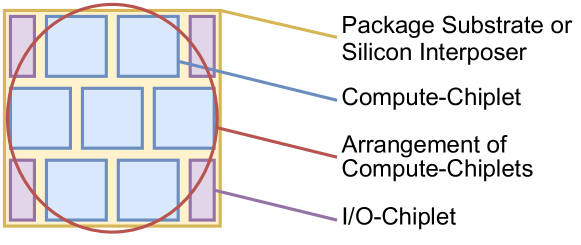
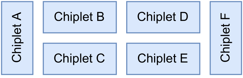
We assume that our chip consists of several identical compute-chiplets and additional chiplets for I/O drivers or other functions. We limit our scope to the search for shape and arrangement of the identical compute-chiplets. Whenever we propose a shape and arrangement of compute-chiplets, we implicitly assume that the remaining chiplets are placed on the perimeter of our arrangement (see Figure 2). Placing the I/O drivers close to the border of the chip is favorable because usually, only solder balls at the border of the package are used for signals. As it is hard to route PCB lanes to solder balls at the center of the package, those solder balls are often used for the power supply.
III-B Constraints for Chiplet Shapes
To ensure that we only consider designs that are economical and easy to manufacture, we identify constraints for the shape of chiplets.
-
•
Uniform Chiplets: All compute-chiplets in a given arrangement must have the same shape and size. Integrating the same functionality into multiple chiplets with different shapes is technologically feasible, however, designing multiple compute-chiplets for a single product generation would increase the non-recurring cost and diminish the economical advantages of 2.5D integration.
-
•
Rectangular Chiplets: All chiplets must be rectangular. Dicing methods such as stealth dicing [stealth-dicing] or plasma dicing [plasma-dicing] enable the fabrication of non-rectangular chiplets. However, the most common dicing method is blade dicing which can only produce rectangular chiplets. By limiting our search to rectangular chiplets, we ensure that we only consider designs with a wide range of applicability.
III-C Proxies for Inter-Chiplet Interconnect Performance
How a given arrangement of chiplets translates into performance (latency and throughput) of the ICI is not obvious. We could run simulations, but this would force us to make many assumptions, e.g., on the bump pitch, chiplet area, or ICI communication protocol details. To be able to predict the performance of an arrangement of chiplets without making any assumptions, we introduce performance proxies.
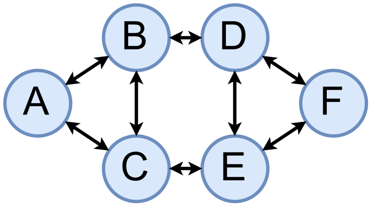
As discussed in Section I, we want to minimize the length of D2D links which implies that only adjacent chiplets can be connected. To be more precise, we define that only chiplets sharing a common edge can be connected. We do not allow links between chiplets that only share a common corner as this would increase the link length. Based on this definition, we represent our 2.5D stacked chip as a planar graph [graphs] where vertices correspond to chiplets and edges correspond to links. Two vertices are connected by an edge whenever the corresponding chiplets are adjacent (see Figure 3).
We use a 2.5D stacked chip’s graph representation to obtain proxies for the latency and global throughput of the ICI. Whenever a flit111Flow control unit: Atomic amount of data transported across the network. transitions from a chiplet to the interposer or vice-versa, it needs to be processed by a PHY which adds a certain latency. Based on this observation, we use the diameter of a chip’s graph representation as a proxy for its latency and we use the bisection bandwidth of the graph representation as a proxy for the global throughput.
III-D Problem Statement
In this work, we want to solve the following problem:
Find a shape and arrangement of chiplets that maximizes the proxies for inter-chiplet interconnect performance as defined in Section III-C while satisfying all constraints from Section III-B.
Neighbors: Min: 2, Max: 4.
Diameter: .
Bisection BW: .

Neighbors: Min: 2, Max: 6.
Diameter: .
Bisection BW: .

Neighbors: Min: 2, Max: 6.
Diameter: .
Bisection BW: .

Neighbors: Min: 3, Max: 6.
Diameter: .
Bisection BW: .
IV Enhancing Shape and Arrangement of Chiplets
We now illustrate a novel arrangement of chiplets, the HexaMesh (HM), which enhances the performance of the ICI while maintaining ease of manufacturing. For this, we first observe that the most straightforward way to build a 2.5D stacked chip is arranging chiplets in a 2D grid (G), which we use as the main baseline. We illustrate how to go through multiple improvements of a G until we arrive at the HM. For each arrangement, we deliver a shape of chiplets and a placement of C4 bumps or micro-bumps that minimizes the length of D2D links. Finally, we discuss how to apply arrangements to arbitrary chiplet counts and we compare multiple arrangements in terms of their network diameter and bisection bandwidth (performance proxies).
IV-A Optimizing the Arrangement of Chiplets
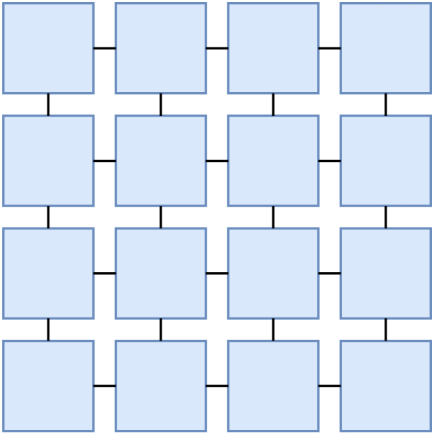
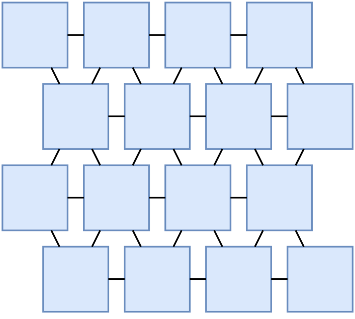
Grid (G)
We show a 2D grid in Figure 4(a). We observe that each non-border chiplet is connected to four other chiplets. Mathematically speaking, the average number of neighbors per chiplet goes to four as the number of chiplets goes to infinity. Intuitively, increasing the average number of neighbors per chiplet should reduce the network diameter and increase the bisection bandwidth.
To explore arrangements that maximize the average number of neighbors per chiplet, we drop the constraint that chiplets need to be rectangular for the next paragraph. In the subsequent paragraph, we show how to fix this violation of constraints.
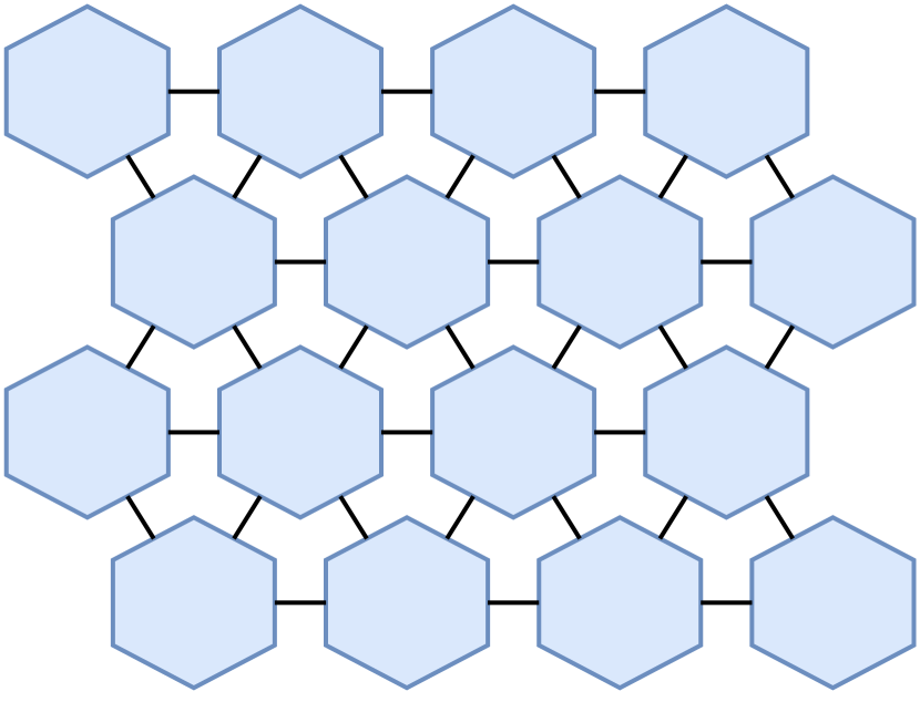
Honeycomb (HC)
If we manufacture hexagonal chiplets and arrange them in a honeycomb pattern, then, each non-border chiplet is connected to six other chiplets (see Figure 4(b)). The average number of neighbors per chiplet approaches six as the number of chiplets goes to infinity. As we have seen in Section III-C, we can represent each arrangement of chiplets as a planar graph (a graph that can be drawn such that no edges cross each other). A fundamental theorem of graph theory states that for planar graphs with vertices and edges, does hold. We use this inequality to derive an upper bound for the average vertex degree in planar graphs, which corresponds to the average number of neighbors per chiplet:
Asymptotically speaking, the honeycomb (HC) maximizes the average number of neighbors per chiplet. However, it does violate our constraints since it uses non-rectangular chiplets.
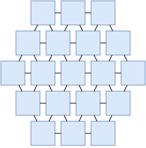
Brickwall (BW)
Arranging rectangular chiplets in a brickwall pattern (see Figure 4(c)) results in the same graph structure as the HC. This enables an asymptotically optimal average number of neighbors per chiplet without violating any constraints on the shape of chiplets.
HexaMesh (HM)
We want to further optimize our arrangement of chiplets. One issue in the brickwall (BW) is that there are two chiplets with only two neighbors. By arranging chiplets in a circle around one central chiplet (see Figure 4(d)), we can increase the minimum number of neighbors per chiplet from to . An additional advantage of this arrangement is that it asymptotically reduces the network diameter by compared to the BW (see Section IV-D for details).
As the HC violates our constraints and the BW results in the same graph structure, we only consider the G, BW, and HM from now on.
IV-B Optimizing the Shape of Chiplets
For each arrangement that we discussed above, we find a shape of chiplets that maximizes the performance of the ICI.
Recall that the ICI is built using D2D links which are attached to chiplets using C4 bumps or micro-bumps. The bandwidth of a link is larger if the link has more bumps at its disposal. The maximum number of bumps per chiplet is proportional to the chiplet area . A fraction of these bumps is used for the chiplet’s power supply and the remaining bumps are used for D2D links. We divide the area of a chiplet into different sectors. Each sector contains bumps used for either the power supply or for one of the D2D links (see Figure 5). To make sure that all links have the same bandwidth, all sectors for bumps of D2D links must have the same area .
The second shape-related factor that influences the performance of the ICI is the length of D2D links. To minimize the link length, we minimize the maximum distance between a bump and the edge of the chiplet (see Figure 5). To minimize , we place the sector containing power bumps in the center of the chiplet and we place the sectors for bumps of D2D links at the chiplet edges. To make sure that all D2D links have the same performance, we enforce that the distance is identical for all sectors containing link bumps.
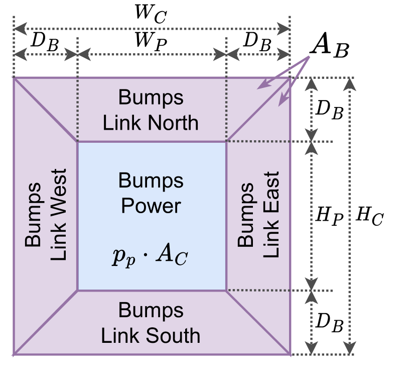
Grid (G)
Figure 5(a) displays how we arrange C4 bumps or micro-bumps in chiplets of the G. The measurements annotated in said figure guarantee that the maximum distance between a bump and the edge of the chiplet is identical for all links. To guarantee that all sectors for link bumps have the same area , we require that the chiplets are square () which implies that the sector for power-bumps is square (). The area of one sector for bumps of a D2D links is and the maximum distance between a bump and the edge of the chiplet is .
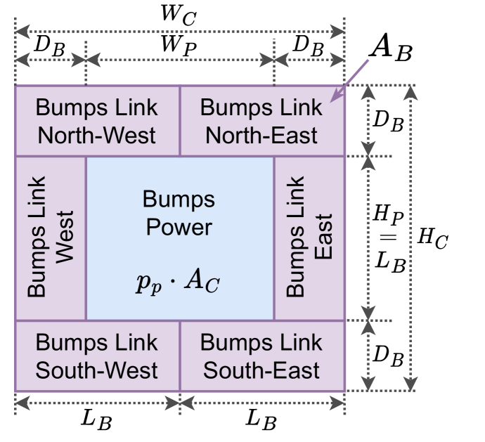
Brickwall (BW) and HexaMesh (HM)
For the BW and HM, we arrange the C4 bumps or micro-bumps as displayed in Figure 5(b). Similarly to the G, the measurements annotated in said figure guarantee that both the area of each sector for link bumps and the maximum distance between a link bump and the edge of the chiplet are identical for all D2D links. The area available for bumps of a given link is . Computing the maximum distance between a link bump and the edge of the chiplet as well as the resulting chiplet dimensions is a bit more involved. Based on Figure 5(b), we set up the following system of equations:
| (1) |
| (2) |
| (3) |
| (4) |
| (5) |
By solving this system of equations, we get the chiplet dimensions and as well as the maximum distance between a bump and the edge of the chiplet:
Consider an example design with a chiplet area of mm2 where a fraction of all bumps are needed for the power supply. Our equations yield the chiplet dimensions mm and mm and a maximum distance of mm between a bump used for D2D links and the chiplet edge.
IV-C Applicability of Arrangements
To apply the G or BW as depicted in Figure 4, the number of chiplets needs to be a square number and for the HM, we need to have for some (if there are rings around the central chiplet where the -th ring contains chiplets, then, we have chiplets in total). We call such an arrangement regular. For the G and BW, we could also use rows and columns of chiplets such that , but which results in a rectangular, non-square shape. We call this a semi-regular arrangement. Semi-regular arrangements make only sense if and are similar, otherwise, both diameter and bisection bandwidth deteriorate. We conclude that for many chiplet-counts, there is no regular or no reasonable semi-regular arrangement. This is a problem as we want to set the number of chiplets based on technological and economical factors, not their desired arrangement.
To solve this problem, we introduce irregular arrangements. Starting from the closest smaller regular arrangement, we incrementally add more chiplets until the desired chiplet-count is reached. In the case of the G and BW, these additional chiplets form incomplete rows or columns, and in the case of the HM, they form an incomplete circle.
For regular and semi-regular G and BW of chiplets, the minimum number of neighbors per chiplet is , and for regular HM of chiplets, the minimum number of neighbors per chiplet is . Introducing irregular arrangements reduces the minimum number of neighbors per chiplet to for some G and to for some HM. This suggests that irregular G and HM might have slightly lower performance compared to their regular peers. Our analysis of performance proxies in Section IV-D will confirm this speculation (see Figure 6).
IV-D Analysis of Performance Proxies
Diameter
The diameter for a regular G, BW, or HM with chiplets can be computed as follows:
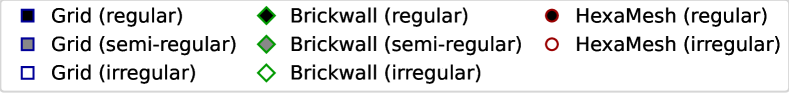
In Figure 6(a), we compare the diameter of all three arrangements for chiplet counts from to . The BW has a significantly lower diameter than the G, and the HM further reduces the diameter. We observe that regular and semi-regular G and HM provide the highest chiplet-count for a given diameter. For the BW, regular and semi-regular arrangements do not seem to have advantages over their irregular peers. To analyze the asymptotic behavior of the diameter of regular arrangements, we compute and . We conclude that asymptotically, the BW reduces the diameter by and the HM reduces the diameter by compared to the G.
Bisection Bandwidth
The bisection bandwidth of a regular G, BW, or HM with chiplets is computed as follows:
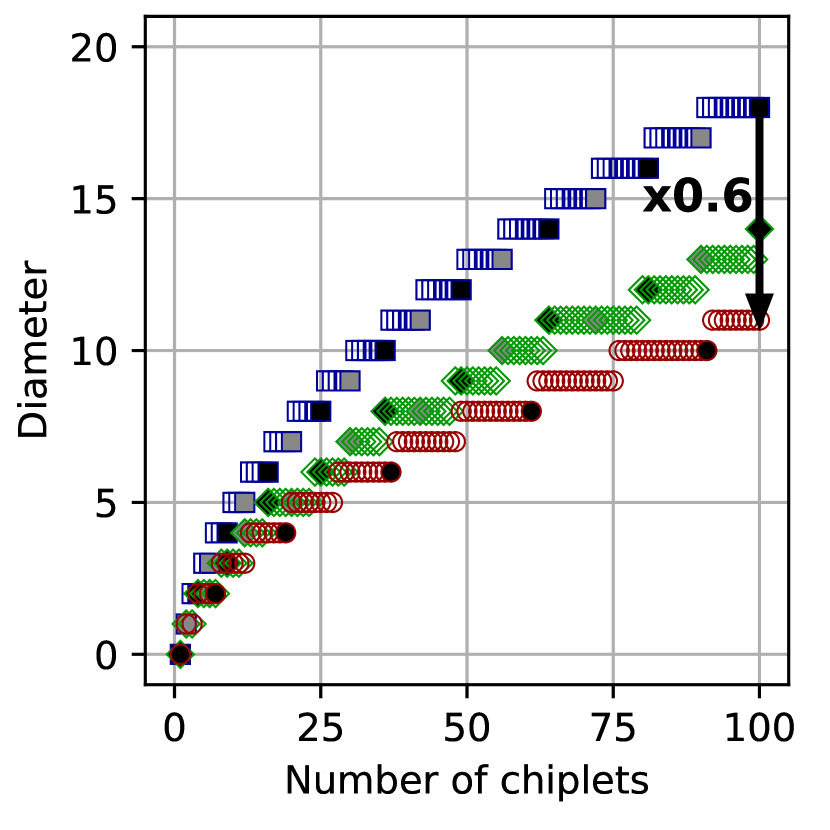
Figure 6(b) compares the bisection bandwidth of all three arrangements for chiplet counts from to . The bisection bandwidth of regular arrangements is computed using the formulas above, that of semi-regular or irregular arrangements is estimated using METIS [metis]. The BW comes with a significantly higher bisection bandwidth compared to the G and the HM further improves upon the BW. To analyze the asymptotic behavior of the bisection bandwidth of regular arrangements, we compute and . Asymptotically, the BW improves the bisection bandwidth by and the HM improves it by compared to the G.
V A Model for D2D Links
The bisection bandwidth is an incomplete proxy for the global throughput, as it only considers the number of links, but not their bandwidth. Since the BW and HM have more D2D links per chiplet than the G, the number of C4 bumps or micro-bumps per link and hence the per-link bandwidth is lower for them. To estimate the link bandwidth for a given arrangement, we introduce our D2D link model.
V-A Model Inputs
Table I lists the architectural parameters that our model needs as inputs to estimate the bandwidth of D2D links.
| Symbol | Description |
| Area (in mm2) available for C4 bumps/micro-bumps of one D2D link | |
| Pitch (in mm) of a C4 bump/micro-bump | |
| Number of non-data wires needed for a D2D link (e.g., wires for handshake, clock, etc.) | |
| Frequency at which the D2D links are operated |
V-B Link Bandwidth Estimation
We start by estimating the number of wires that can be built between the two chiplets. To compute we divide the area available for C4 bumps/micro-bumps by the squared pitch of said bumps. This estimate assumes a regular layout of bumps. A staggered layout would result in a slightly larger number of wires. To get the number of data wires we subtract the number of non-data wires from the number of wires . To estimate the link bandwidth , we multiply the number of data wires by the link frequency .
In practice, the maximum operating frequency of D2D links depends on the length of said links. In this work, we only consider D2D links between adjacent chiplets, whose lengths are relatively short (below mm in general, for chiplets even below mm). Therefore, we make the operating frequency an input parameter rather than computing it based on the link’s physical characteristics.

VI Evaluation
We leverage our model for D2D links and network simulations in BookSim2 [booksim] to compare the ICI performance of different arrangements of chiplets. Many parameters used in this section are based on the UCIe protocol specifications [ucie].
VI-A Cycle-Accurate Simulations using BookSim2
We use the established, cycle-accurate BookSim2 [booksim] network-on-chip simulator to estimate the latency and throughput of different chiplet arrangements. The graph representation (see Section III-C) of a given arrangement is used as an input to BookSim2. We assume that each chiplet contains two endpoints and one local router. This router can route packets between the chiplet’s PHYs or between a PHY and an endpoint. We configure a link-latency of cycles which models the combined latency of the outgoing PHY, the D2D link, and the incoming PHY (UCIe [ucie] states a PHY latency of - UI). Each router has a latency of cycles, virtual channels, and flit buffers.
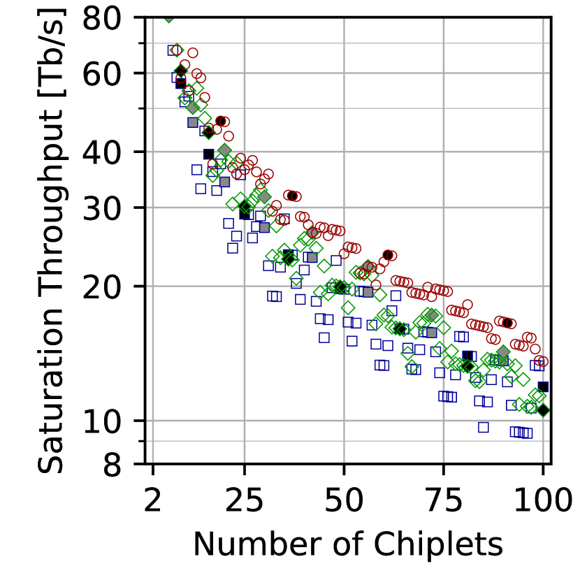
BookSim2 reports the average packet latency and the saturation throughput as the percentage of the full global bandwidth. The full global bandwidth is the maximum theoretical cumulative throughput when all endpoints inject packets in the network at full rate; in our setting, it is the product of the chiplet count, the number of endpoints per chiplet, and the per-link bandwidth which we estimate using our model for D2D links (see next paragraph). We multiply the reported relative throughput by the full global bandwidth of the corresponding arrangement to get the saturation throughput in Tb/s.
VI-B Link Bandwidth Estimation using our Model
We use our model for D2D links to estimate the per-link bandwidth in different arrangements of chiplets. To do this, we need to specify a set of architectural parameters. We assume that the combined area of all chiplets is mm2 which is slightly below the lithographic reticle limit. For an arrangement of chiplets, we compute the chiplet area as . We assume that any chiplet needs a fraction of all C4 bumps for its power supply and that C4 bumps have a pitch of mm. Furthermore, we assume that wires per link are needed for handshake and clock (UCIe [ucie] uses clock-, valid- and track-wire per direction plus wires for the side band). Finally, we assume that D2D links are operated at GHz (UCIe [ucie] can be operated at GHz to support its maximum data rate or GT/s). The area available for bumps of a given D2D link is computed using the equations derived in Section IV-B (except for arrangements with chiplets which are hand-optimized).
VI-C Discussion of Results
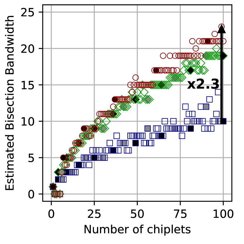
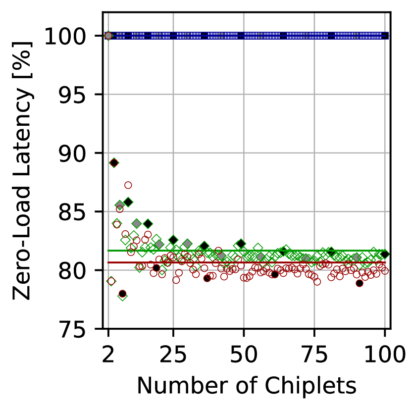
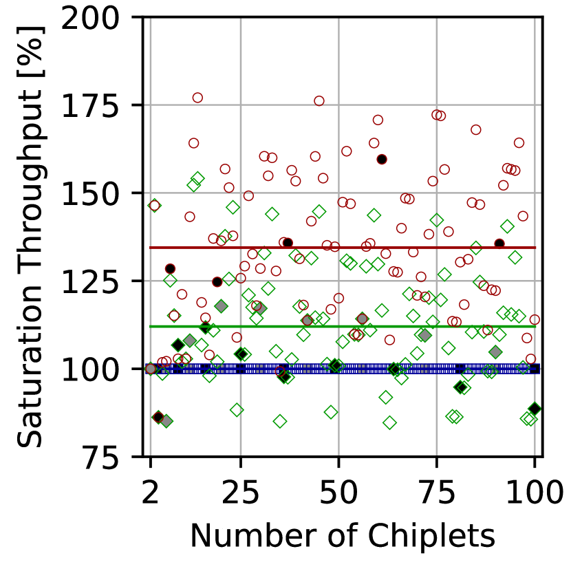
Figures 7(a) and 7(b) show the latency and throughput of the G, BW, and HM, for chiplet counts from to . Figures 7(c) and 7(d) show the latency and throughput of the BW and HM relative to the G (baseline). For chiplets, both the BW and the HM consistently reduce the latency by almost compared to the G. On average, the throughput is increased by if the BW is used and by if the HM is used. We observe that the throughput relative to the G exhibits high fluctuations—this is mainly due to the inconsistent throughput of the G (baseline). Another observation is that in practice (throughput), the BW and HM do not outperform the G by as much as their theoretical superiority (bisection bandwidth) suggests. The cause of this discrepancy is the fact that the BW and HM have more links per chiplet than the G which results in fewer C4 bumps/micro-bumps per link and hence a lower per-link bandwidth compared to the G. This difference in bandwidth is accounted for in the simulations yielding the throughput but not in the theoretical analysis yielding the bisection bandwidth. Nevertheless, we see that by using the HM, we can significantly reduce the latency and significantly improve the throughput without adding any additional manufacturing complexity.
VII Related Work
AMD [amd-chiplets] shows how to use 2.5D integration to solve the economical challenges of technology scaling in production chips. Since they use no more than eight compute-chiplets per chip, they can hand-optimize their chiplet arrangement. In Tesla’s Dojo training tile [dojo] with chiplets where hand-optimizing the chiplet arrangement most likely is infeasible, a 2D grid arrangement with a 2D mesh topology is used. The mesh only connects adjacent chiplets which results in short links with high operating frequencies. Kite [kite] is an ICI topology for 2D grid arrangements where non-adjacent chiplets are connected if the topological advantages of longer links outweigh their disadvantages due to a lower operating frequency. By introducing HexaMesh, we achieve a low network diameter and a high bisection bandwidth while only connecting adjacent chiplets. This means that we can get rid of the mesh’s disadvantages (limited performance) while keeping its advantages (short, high-frequency links). Coskun et al. [placement-opt] introduce a cross-layer co-optimization approach for ICI design and chiplet arrangement. For a set of existing topologies, they optimize the chiplet arrangement to maximize ICI performance and minimize manufacturing cost and operating temperature. In their approach, the chiplet arrangement depends on the topology while in our approach the topology depends on the chiplet arrangement (we connect adjacent chiplets). The advantage of our approach is that by only connecting adjacent chiplets, we minimize the length of D2D links which maximizes their operating frequency. There are many works in the 2.5D integration landscape that provide contributions orthogonal to ours. Chiplet Actuary [chiplet-actuary] for example provides a detailed cost model to analyze the economical benefits of disaggregation. This cost model could be applied together with our evaluation methodology to compare architectures both in terms of cost (Chiplet Actuary) and performance (our methodology). Dehlaghi et al. [usr-links] provide a detailed model to estimate the insertion loss and crosstalk of ultra-short reach (USR) D2D links. Their work could be used to extend our model for D2D links by adding predictions for the bit error rate in addition to our link bandwidth predictions.
VIII Conclusion
2.5D integration is believed to be the solution to the economical challenges of CMOS technology scaling, but it introduces a new challenge: Providing a high-performance inter-chiplet interconnect (ICI). The fact that D2D links need to be short to run at high frequencies strongly limits the choice of ICI topologies.
In this work, we propose HexaMesh, an arrangement of chiplets that reduces the ICI’s network diameter by while increasing its bisection bandwidth by compared to a grid arrangement. Furthermore, we introduce a model to estimate the bandwidth of D2D links which is needed for a fair comparison of designs with varying numbers of links per chiplet. Our evaluations show that HexaMesh is not only superior to a grid arrangement in theory but also in practice, as it reduces the latency by on average and improves the throughput by on average. HexaMesh uses uniform and rectangular chiplets, which ensures that employing the HexaMesh arrangement does not increase the complexity of designing or manufacturing a chip.
Acknowledgements
This work was supported by the ETH Future Computing Laboratory (EFCL), financed by a donation from Huawei Technologies.
It also received funding from the European Research Council
![]() (Project PSAP,
No. 101002047) and from the European Union’s HE research
and innovation programme under the grant agreement No. 101070141 (Project GLACIATION).
We thank Timo Schneider for help with computing infrastructure at SPCL.
(Project PSAP,
No. 101002047) and from the European Union’s HE research
and innovation programme under the grant agreement No. 101070141 (Project GLACIATION).
We thank Timo Schneider for help with computing infrastructure at SPCL.
References
- [1] T. Li, J. Hou, J. Yan, R. Liu, H. Yang, and Z. Sun, “Chiplet heterogeneous integration technology—status and challenges,” Electronics, vol. 9, no. 4, p. 670, 2020.
- [2] G. E. Moore et al., “Cramming more components onto integrated circuits,” 1965.
- [3] S. Mirabbasi, L. C. Fujino, and K. C. Smith, “Through the looking glass—the 2022 edition: Trends in solid-state circuits from ISSCC,” IEEE Solid-State Circuits Magazine, vol. 14, no. 1, pp. 54–72, 2022.
- [4] S. Naffziger, N. Beck, T. Burd, K. Lepak, G. H. Loh, M. Subramony, and S. White, “Pioneering chiplet technology and design for the AMD EPYC™ and RYZEN™ processor families: Industrial product,” in 2021 ACM/IEEE 48th Annual International Symposium on Computer Architecture (ISCA). IEEE, 2021, pp. 57–70.
- [5] “Bunch of wires (bow) phy specification,” https://opencomputeproject.github.io/ODSA-BoW/bow_specification.html.
- [6] “Universal Chiplet Interconnect Express (UCIe) Specification,” https://www.uciexpress.org/specification.
- [7] N. Jiang, D. U. Becker, G. Michelogiannakis, J. Balfour, B. Towles, D. E. Shaw, J. Kim, and W. J. Dally, “A detailed and flexible cycle-accurate network-on-chip simulator,” in 2013 IEEE international symposium on performance analysis of systems and software (ISPASS). IEEE, 2013.
- [8] P. Vivet, E. Guthmuller, Y. Thonnart, G. Pillonnet, C. Fuguet, I. Miro-Panades, G. Moritz, J. Durupt, C. Bernard, D. Varreau et al., “IntAct: A 96-core processor with six chiplets 3D-stacked on an active interposer with distributed interconnects and integrated power management,” IEEE Journal of Solid-State Circuits, vol. 56, no. 1, pp. 79–97, 2020.
- [9] B. Dehlaghi, N. Wary, and T. C. Carusone, “Ultra-short-reach interconnects for die-to-die links: Global bandwidth demands in microcosm,” IEEE Solid-State Circuits Magazine, vol. 11, no. 2, pp. 42–53, 2019.
- [10] M. Kumagai, N. Uchiyama, E. Ohmura, R. Sugiura, K. Atsumi, and K. Fukumitsu, “Advanced dicing technology for semiconductor wafer—stealth dicing,” IEEE Transactions on Semiconductor Manufacturing, vol. 20, no. 3, pp. 259–265, 2007.
- [11] N. Matsubara, R. Windemuth, H. Mitsuru, and H. Atsushi, “Plasma dicing technology,” in 2012 4th Electronic System-Integration Technology Conference. IEEE, 2012, pp. 1–5.
- [12] D. B. West et al., Introduction to graph theory. Prentice Hall Upper Saddle River, 2001, vol. 2.
- [13] G. Karypis and V. Kumar, “Metis: A software package for partitioning unstructured graphs, partitioning meshes, and computing fill-reducing orderings of sparse matrices,” 1997.
- [14] E. Talpes, D. Williams, and D. Das Sarma, “DOJO: The Microarchitecture of Tesla’s Exa-Scale Computer,” in 2022 IEEE Hot Chips 34 Symposium (HCS), IEEE. IEEE, 2022, pp. 1–28.
- [15] S. Bharadwaj, J. Yin, B. Beckmann, and T. Krishna, “Kite: A family of heterogeneous interposer topologies enabled via accurate interconnect modeling,” in 2020 57th ACM/IEEE Design Automation Conference (DAC). IEEE, 2020, pp. 1–6.
- [16] A. Coskun, F. Eris, A. Joshi, A. B. Kahng, Y. Ma, A. Narayan, and V. Srinivas, “Cross-layer co-optimization of network design and chiplet placement in 2.5-D systems,” IEEE Transactions on Computer-Aided Design of Integrated Circuits and Systems, vol. 39, no. 12, pp. 5183–5196, 2020.
- [17] Y. Feng and K. Ma, “Chiplet actuary: A quantitative cost model and multi-chiplet architecture exploration,” arXiv preprint, 2022.