Sparse Hamming Graph:
A Customizable Network-on-Chip Topology
Abstract
Chips with hundreds to thousands of cores require scalable networks-on-chip (NoCs). Customization of the NoC topology is necessary to reach the diverse design goals of different chips. We introduce sparse Hamming graph, a novel NoC topology with an adjustable cost-performance trade-off that is based on four NoC topology design principles we identified. To efficiently customize this topology, we develop a toolchain that leverages approximate floorplanning and link routing to deliver fast and accurate cost and performance predictions. We demonstrate how to use our methodology to achieve desired cost-performance trade-offs while outperforming established topologies in cost, performance, or both.
I Introduction
CMOS technology scaling keeps increasing the transistor density, enabling the integration of a growing number of compute cores into modern processors and accelerators. While the parallel performance of such architectures is skyrocketing, more and more applications are becoming bound by data movement [1, 2, 3, 4, 5, 6]. This includes traditional graph processing kernels [7, 8, 9], dense linear algebra kernels [10, 11, 12], complex pattern matching applications [13, 14, 15, 16, 17, 18, 19, 20], but also newer classes of mixed sparse-dense workloads such as graph neural networks [21, 22, 23, 24, 25]. These developments stress the importance of scalable, high-performance networks-on-chip (NoCs).
A key decision to make when designing a network-on-chip (NoC) is the choice of a suitable topology of links between routers. The NoC topology has a large influence on the NoC’s performance (latency, throughput) and cost (area, power). To guide the design of low-cost and high-performance NoC topologies, we identify four fundamental NoC topology design principles (Section II, contribution #1). To achieve low cost, ❶ use low-radix topologies and ❷ design for link routability and to achieve high performance, ❸ minimize the network diameter and ❹ minimize the physical path length111The total physical distance that the data travels across the chip.. Principle ❶ minimizes the router area and the overall number of links and principle ❷ minimizes the area overhead induced by links - both minimizing the NoC’s cost. Principle ❸ minimizes the number of router-to-router hops per flit (minimize latency) and hence the number of flits processed by a given router (minimize congestion maximize throughput). Principle ❹ minimizes the latency which is linear in the physical path length.
Achieving a low network diameter (following ❸ ) requires a high router radix (violating ❶) and vice versa. Hence, no single topology can provide high-performance and low-cost, instead, a trade-off between the two is needed. To meet the diverse requirements of different architectures, the NoC topology’s cost-performance trade-off must be adjustable. We introduce sparse Hamming graph, a customizable NoC topology that is based on our NoC topology design principles (Section III, contribution #2). By adjusting the sparsity of links in the topology, we can steer its cost-performance trade-off.
Different architectures do not only differ in their design goals (e.g., low-power vs. high-performance) but also in their architectural parameters (e.g., number and size of cores, technology node, or transport protocol). We want to adjust the sparsity of the sparse Hamming graph topology to both, the design goals and the architectural parameters. To do this, we need a way to predict the performance and cost that a NoC topology attains if applied to a given architecture. Existing models for cost and performance predictions can be grouped into high-level and low-level models. High-level models are fast, but they do not consider implementation details like, e.g., link routing, which results in a lack of accuracy. Low-level models are accurate but extremely time-consuming which renders them unwieldy for a quick exploration of a large design space. To bridge the gap between high-level and low-level models, we develop a novel, custom cost and performance prediction toolchain222Source code: https://spclgitlab.ethz.ch/iffp1/sparse_hamming_graph_public (Section IV, contribution #3). Our toolchain works at the speed of high-level models but other than existing high-level models, it estimates implementation-details by performing approximate floorplanning and link routing.
To evaluate the proposed NoC topology customization strategy, we use our prediction toolchain to rapidly customize four sparse Hamming graph topologies for four different architectures, each with its unique set of architectural parameters. The design goal is to maximize each NoC’s performance without dedicating more than of the total chip area to it. Our evaluation (Section V) shows that our customized sparse Hamming graph topologies outperform established topologies in terms of cost, performance, or both.
II Design Principles for NoC Topologies
Links form a cycle.
Neighboring tiles are connected.
Rows/columns form a cycle.
2D torus without long links.
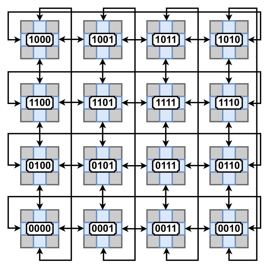
Connect tiles if IDs differ in 1 bit.
Topology based on MMS graphs.
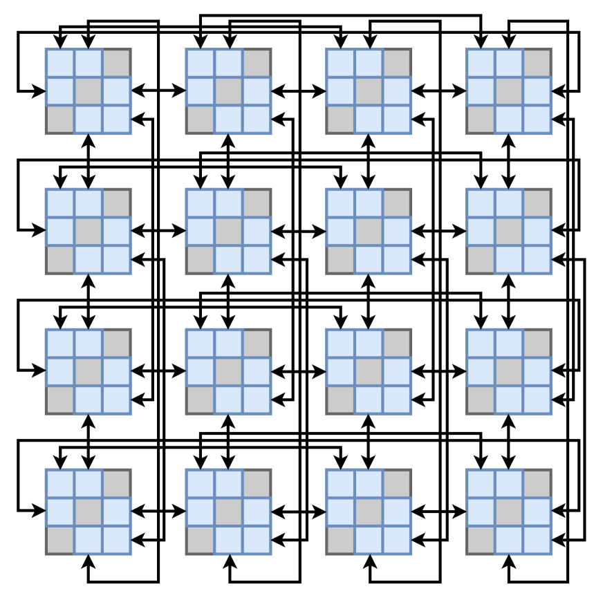
Fully-connected rows/columns.
II-A Assumptions
Throughout the whole paper, we assume a chip that is organized as an grid of identical building blocks which we call tiles. Each tile contains one or more endpoints (e.g., compute cores or memories) and a local router to which all of its endpoints are connected. A NoC is used to provide connectivity between different tiles. The NoC’s links are attached to the tile’s local routers. This regular tiled design is common for large compute fabrics as its modularity keeps the physical design effort at the top level under control. We assume that each metal layer has a predefined routing direction. Furthermore, whenever a link is too long to be operated at the target clock frequency, we insert as many registers (pipeline stages) as necessary to meet said frequency. As a result, sending a flit across a link can take multiple clock cycles [27] which means that we need network components [28, 29] capable of handling multi-cycle links. Finally, we assume that tiles occupy all available metal layers which disallows routing an inter-tile link between two tiles and over a third tile .
II-B Reduce Cost (Area, Power)
The following two design principles aim at reducing the NoC’s area. Since a chip’s power consumption is roughly linear in its area [30], following these design principles also reduces the power consumption.
The area of most router architectures scales quadratically with the router radix [31], hence, high-radix topologies come with large area requirements. Additionally, in a setting with one router per tile, a higher router radix implies a higher overall number of links which further inflates the NoC’s area.
When designing a NoC topology, it is crucial to pay attention to the routability of links which can be improved by meeting the following four criteria:
-
•
Short Links: Links between adjacent tiles come with minuscule area overheads while long links occupy a large area.
-
•
Aligned Links: Links between tiles in the same row or column tend to be more area-efficient than links that change row and column.
-
•
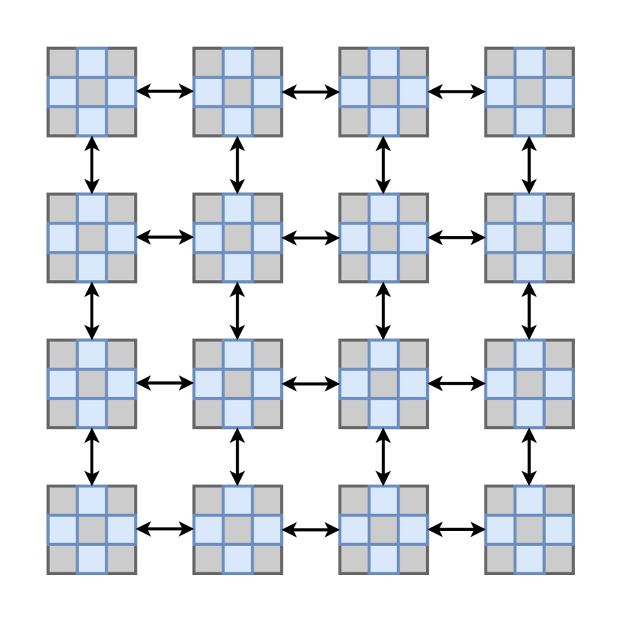
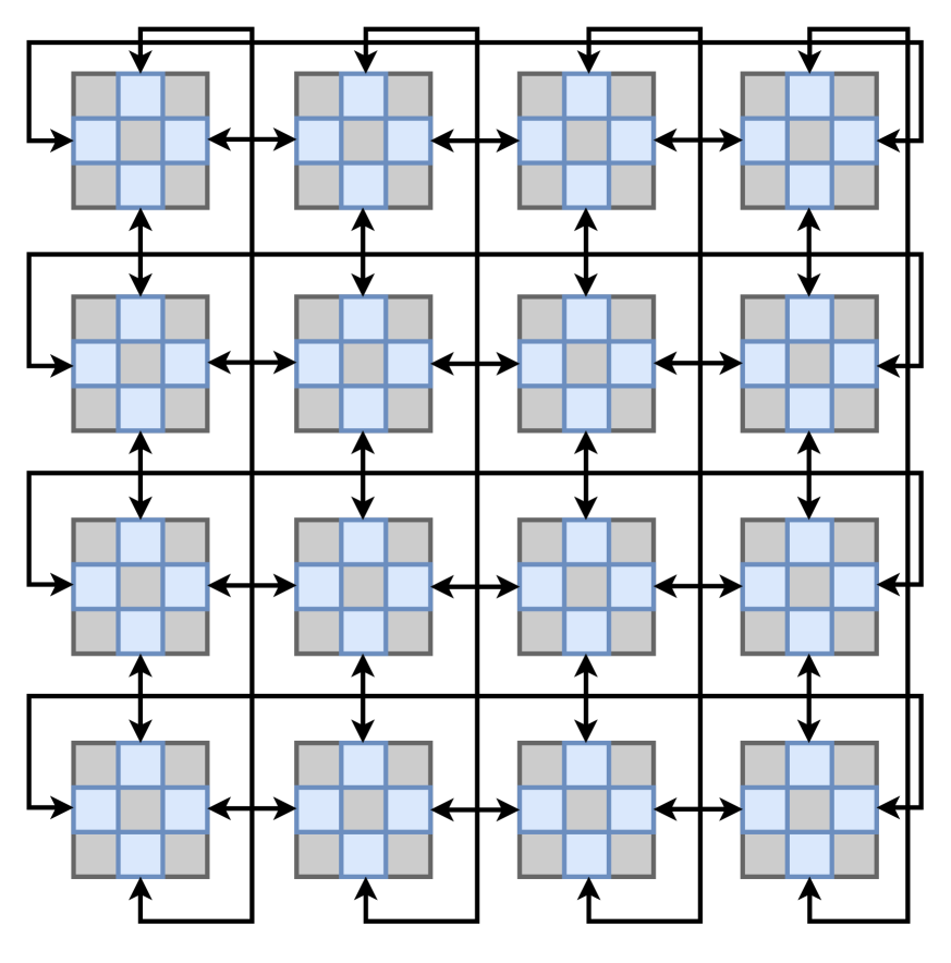
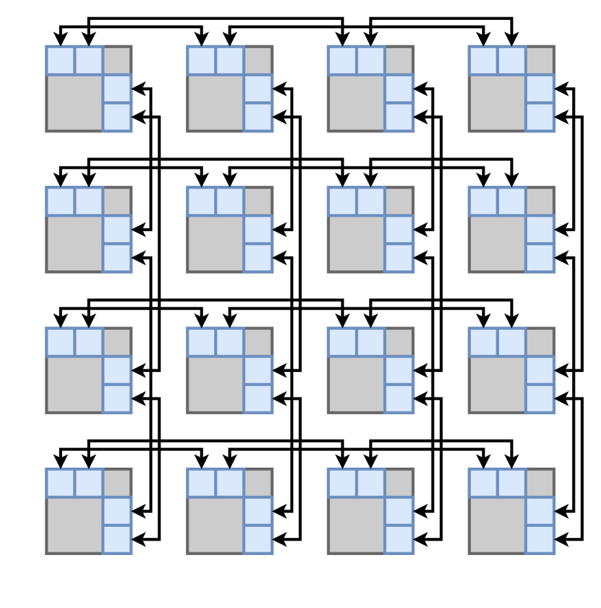
Uniform Link Density: Assume that the space between two rows or columns of tiles contains sections with high and sections with low link density (like, e.g., SlimNoC, see Figure 1(f)). The spacing between said rows or columns needs to be large enough to fit all links from the high-density section, resulting in an under-utilization of the low-density section. To use the area efficiently, we should aim for a uniform link density (like, e.g., 2D torus, see Figure 1(c)).
-
•
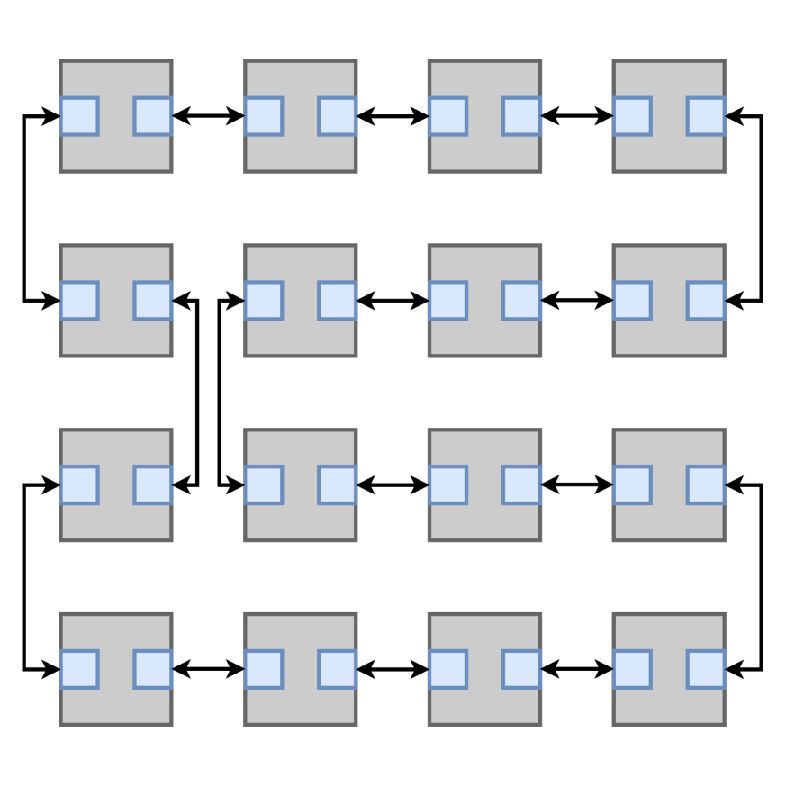
Optimized Port Placement: The location of ports within a tile influences the routability of links. E.g., for a mesh topology, we can place one port on each face of the tile which results in short, straight links between tiles (see Figure 1(b)). In the ring topology on the other hand, the ports are placed north/south or east/west which both inflates the lengths of a subset of links (see Figure 1(a)).
II-C Boost Performance (Latency, Throughput)
The network diameter is the maximum number of routers-to-router hops that a flit333Flow control unit: Atomic amount of data transported across the network. takes on the path from its source-tile to its destination-tile. Whenever a flit traverses a router, it experiences a certain delay, therefore, minimizing the network diameter reduces the latency. Furthermore, a reduction of the average number of router-to-router hops per flit goes along with a reduction of the average number of flits processed by a given router which reduces the congestion at routers and improves the throughput.
The delay of a link built of buffered wires is linear in its length [30]. As a consequence, minimizing the physical distance that a flit travels is crucial to achieve low latency. The prerequisite for using paths of minimal physical length is the existence of links that provide such paths. However, the pure existence of these links is not enough since the routing algorithm might send flits over physically non-shortest paths. This could for example happen if the routing algorithm minimizes the number of router-to-router hops, which does not necessarily minimize the physical path length. Adapting the routing algorithm to minimize the physical path length is not the solution since, e.g., in a 2D torus topology (see Figure 1(c)), this would leave the wrap-around links unused and severely deteriorate the throughput. To provide low latency while sustaining high throughput, a NoC topology should a) contain links that provide physically minimal paths and b) be co-designed with the routing algorithm to use these paths without reducing the throughput.
III The Sparse Hamming Graph NoC Topology
| Topology | Router Radix | Design for Routability | Network Diameter | Minimal Paths∗ | #Configurations for given and | ||||
| SL | AL | ULD | OPP | Present∗∗ | Used∗∗∗ | ||||
| Ring | 2 | ✔ | ✔ | ✘ | ✘ | ✘ | 1 | ||
| 2D Mesh | 4 | ✔ | ✔ | ✔ | ✔ | ✔ | ✔ | 1 | |
| 2D Torus | 4 | ✘ | ✔ | ✔ | ✔ | ✔ | ✘ | 1 | |
| Folded 2D Torus [32] | 4 | ✔ | ✔ | ✔ | ✘ | ✘ | 1 | ||
| Hypercube [33] | ✘ | ✔ | ✔ | ✔ | ✔ | ✘ | 0 or 1† | ||
| SlimNoC [26] | ✘ | ✘ | ✘ | ✘ | ✘ | ✘ | 0 or 1‡ | ||
| Flattened Butterfly [34] | ✘ | ✔ | ✘ | ✔ | ✔ | ✔ | 1 | ||
| Sparse Hamming Graph (This Work) | (✔) | ✔ | (✔) | ✔ | ✔ | (✔) | |||
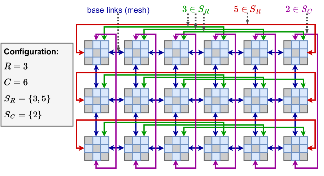
We propose the customizable sparse Hamming graph topology that is based on our four NoC topology design principles. The sparsity of this topology depends on two input parameters which enables an effortless adjustment of its cost-performance trade-off. Table I shows the compliance of sparse Hamming graph and many established NoC topologies with our four NoC topology design principles.
Concept
The base for a sparse Hamming graph is a 2D mesh topology. It fulfills all design for routability criteria (❷ ) and it provides a low router radix (❶) which ensures a low cost. In addition, the mesh topology provides paths with minimal physical length (❹ ) resulting in low latency. The downside of the mesh topology is the relatively high network diameter (❸ ) that leads to significant performance penalties when scaling up the number of tiles. To alleviate this issue, we add additional links to our topology. The number and shape of these additional links are configured through a set of parameters. The way in which we add these links (refer to the next paragraph for details) ensures that a good routability of links (❷ ) is maintained. With the maximum number of additional links, we reach a flattened butterfly topology that provides a low network diameter (❸ ) and excellent performance. The downside of the flattened butterfly is its significant area overhead. In summary, the sparse Hamming graph spans the design space between a mesh topology (low cost) and a flattened butterfly topology (high performance) while following our design principles to ensure reaching favorable cost-performance trade-offs.
Construction
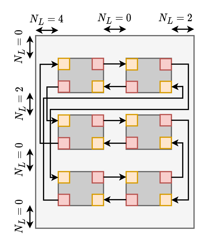
Let and be the number of rows and columns of tiles in our chip. The sparse Hamming graph topology takes two sets as parameters: A set and a set . Let be the tile in row and column . We start with a 2D mesh topology. For each row , for each number and for each number , , we add a link . Likewise, for each column , for each number and for each number , , we add a link . Figure 2 visualizes this construction. Since all topologies that are constructed this way are subgraphs of a 2D Hamming graph, we call this topology sparse Hamming graph.
IV Prediction of Performance and Cost
To efficiently customize the sparse Hamming graph topology to the design goals and architectural parameters at hand, we develop our custom toolchain for performance and cost predictions.
IV-A Overview of Prediction Toolchain
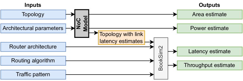
Figure 3 shows our toolchain for NoC performance and cost predictions. We develop a custom model that leverages a set of architectural parameters to estimate the area and power consumption (cost) associated with a given NoC topology. In addition, our model estimates the latency of every router-to-router link in the NoC. We feed the NoC topology with link latency estimates as well as information about the router architecture, routing algorithm, and traffic pattern into the cycle-accurate BookSim2 [35] NoC simulator. Based on the results of the BookSim2 simulations, we estimate the NoC’s zero-load latency and saturation throughput (performance). The key to accurate simulations in BookSim2 are our model’s link latency estimates.
IV-B A Model for Area, Power and Link Latency Prediction
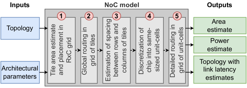
Figure 4 visualizes our model for predicting a NoC’s area overhead, power consumption, and the latency of every router-to-router link. Our model is based on the assumptions stated in Section II-A.
IV-B1 Architectural Parameters
Table II summarizes the architectural parameters that our model takes as inputs. The descriptions in Table II make it straightforward to set most of these parameters. Configuring the functions and that return the channel width (in mm) needed to build horizontal and vertical wires respectively is a bit more involved, therefore, we provide an example. Consider a technology with metal layers. Assume that out of those layers are available for signal routing. Say that out of those layers, are used for horizontal routing and are used for vertical routing. Assume that the horizontal layers have a wire pitch of nm, nm, and nm, and that the vertical layers have a wire pitch of nm and nm. In this scenario, we would configure the following two functions that are explained in the subsequent paragraph:
We start by transforming the wire pitch of each metal layer into the number of wires per nm. To do this, we compute the reciprocal of the wire pitch. Next, we compute the overall number of wires per nm for a given direction which is done by summing up the reciprocal wire pitches of all metal layers for said direction. Then, we divide the number of wires by said sum, which gives us the space (in nm) needed to build wires in a given direction. Finally, we multiply the result by to transform it from nm to mm. This computation allows us to represent multiple physical metal layers with different wire pitches as a single, abstract metal layer.
| Parameters describing the chip design | |
| Number of tiles | |
| Combined area of all endpoints (cores + local memories) in a tile in gate equivalent (GE) | |
| Aspect ratio of a tile (height:width) | |
| Parameters describing the NoC | |
| Frequency at which the NoC is run | |
| Bandwidth of each router-to-router link | |
| Parameters describing the technology node | |
| Function; area (in mm2) needed to synthesize GE of logic. | |
| Function; space (in mm) needed to manufacture parallel, horizontal wires. | |
| Function; space (in mm) needed to manufacture parallel, vertical wires. | |
| Function; approximate power consumption (in W) of mm2 of logic-dominated area. | |
| Function; approximate power consumption (in W) of mm2 of wire-dominated area. | |
| Function; time (in s) it takes a signal to travel a distance of mm along a buffered wire. | |
| Parameters describing the on-chip transport protocol | |
| Function; number of wires needed to build a link with a bandwidth of bits/cycle | |
| Function; area (in GE) of a NoC router with manager ports, subordinate ports and bandwidth | |
IV-B2 Model Details
We describe the five steps to construct our NoC model and how to use it to estimate the NoC’s area overhead, power consumption and the latency of every router-to-router link.


Model Construction
Our model is constructed in five steps:
-
•
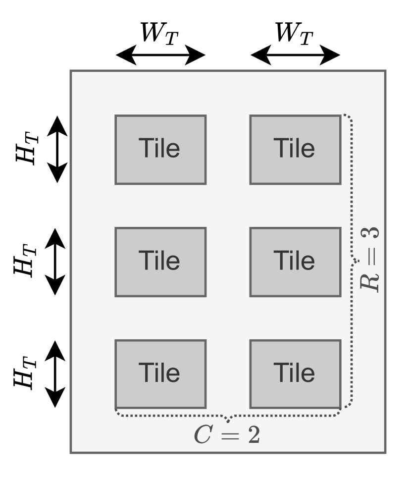
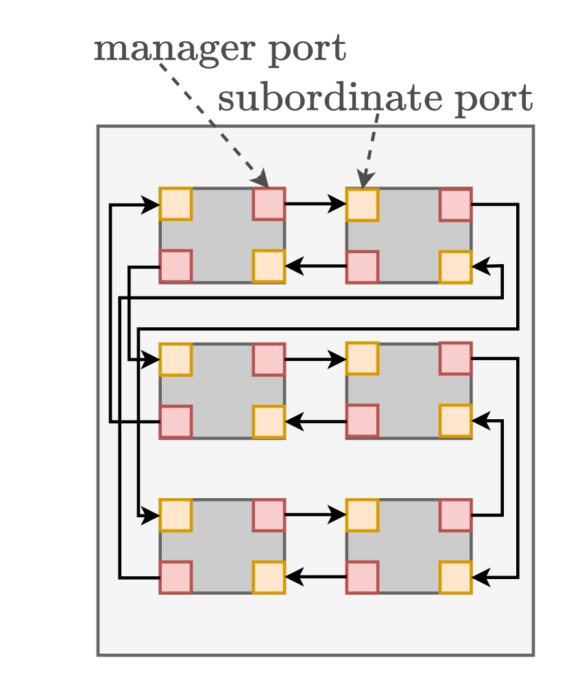
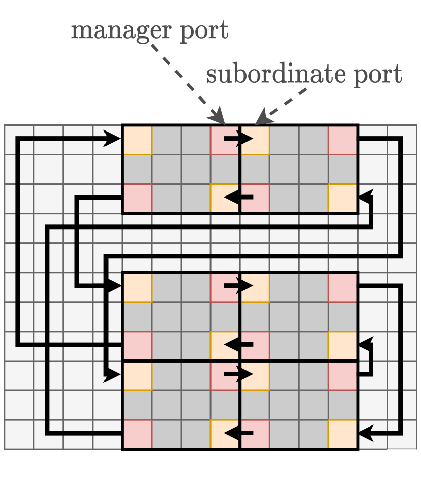
Step 1: Tile Area Estimate and Placement in Grid. We start by estimating the area of a tile as where is the area of the tile’s local router. The router area is computed as where the number of manager-ports and the number of subordinate-ports both depend on the NoC topology. The tile height and width are computed as follows:
The tiles are then arranged in an grid (see Figure 5(a)).
-
•
Step 2: Global Routing in Grid of Tiles. Since we assume that it is not possible to route links on top of tiles, we route them in the space between tiles (see Figure 5(b)). Wire routing in VLSI-design is an NP-complete problem [36], which is tackled using heuristic algorithms. Similarly as in real VLSI-design, we use a greedy algorithm to perform the global routing. Notice that the locations of ports are taken into account in the global routing.
-
•
Step 3: Estimation of Spacing between Rows and Columns of Tiles. If there are at most parallel, horizontal links between two rows of tiles, then the spacing between them is estimated as
To compute the spacing between two columns of tiles with parallel, vertical links in between, is replaced by in the equation above. Figure 5(c) visualizes this step.
-
•
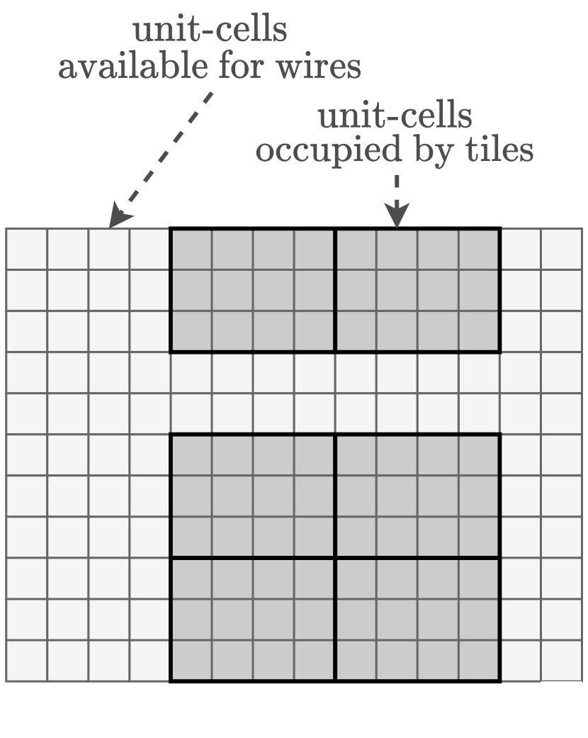
Step 4: Discretization of Chip into same-sized Unit-Cells. To facilitate the detailed routing and the computation of area, power and link latency estimates, we discretize the chip into same-sized unit-cells. The width and the height of a unit-cell are set such that the unit-cell can accommodate exactly one horizontal and one vertical link.
The area of a unit-cell is . Figure 5(d) displays the chip represented as a grid of unit-cells.
-
•
Step 5: Detailed Routing in Grid of Unit-Cells. We use a custom heuristic algorithm to route links in the grid of unit-cells. This algorithm tries to reduce the number of collisions (multiple parallel links in the same unit-cell) and the link lengths (see Figure 5(e)).
Area Estimate
The total area of a chip consisting of unit-cells is . The area that would be necessary to build the chip without a NoC which is
We define the NoC’s area overhead as the percentage of the total chip area that would be saved if we would remove the NoC.
Power Estimate
Let , , and be the number of unit-cells containing logic (a tile), a horizontal part of a link and a vertical part of a link respectively. Notice that a single unit-cell can contribute to both and (if two links are crossing) or it can contribute to none of the three cell-counts (if it is empty). We estimate the chip’s total power consumption as
The power consumption of the chip without a NoC and the NoC’s power consumption are computed as follows:
Link Latency Estimate
We estimate the latency (in clock cycles) of a link that crosses unit-cells vertically and unit-cells horizontally as follows:
IV-C Toolchain Evaluation
To assess the accuracy of our prediction toolchain, we use it to predict the performance and cost of the open-source MemPool [37] architecture. Besides having a complex low-latency interconnect between its cores and memory banks, MemPool also has a long implementation runtime. This makes it a prime target for our model, which can give information about the performance and cost of a certain topology without requiring the long iterative place-and-route flow. Table III shows the cost and performance numbers of MemPool, the predictions of our toolchain, and its prediction error. The area and power predictions are accurate for a fast high-level model. Our model over-estimates the latency of MemPool because MemPool is highly latency-optimized, which breaks our assumptions that each link and each router has a minimum latency of one cycle. To take this into account, we need to deduct cycles from our model estimate ( cycle to inject the flit and cycle for each of the three routers that a given flit traverses). This would result in a latency estimate of cycles, which is only off by . For most designs, our assumptions on the router latency hold, and such corrections are not necessary.
| Metric | Correct Value | Prediction | Prediction Error |
| Area | mm2 | mm2 | % |
| Power | W | W | % |
| Latency | cycles | cycles | % |
| Throughput | % | % | % |
V Application and Evaluation
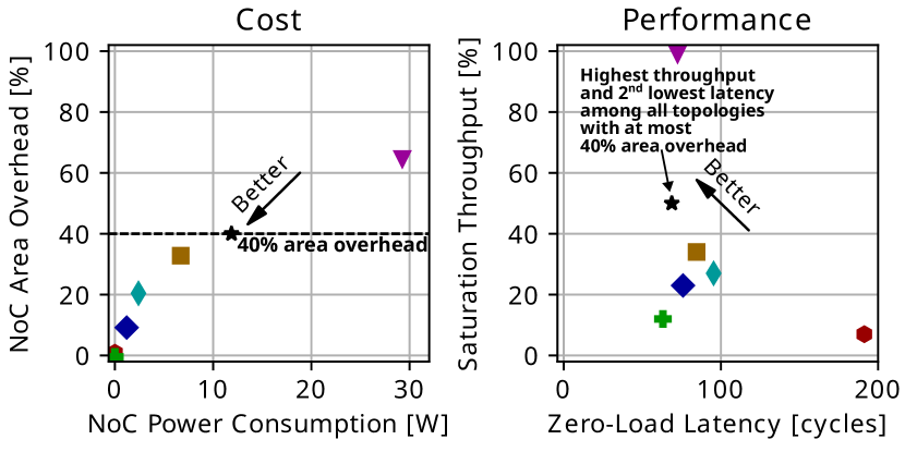
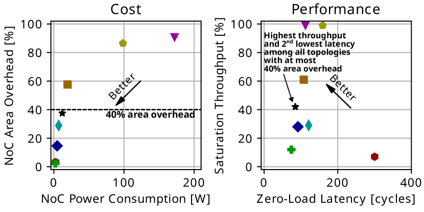
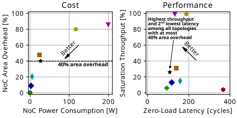
We show how to use our prediction toolchain and design principles to customize the sparse Hamming graph topology. To assess the quality of our customization strategy, we compare customized sparse Hamming graph topologies to a series of established NoC topologies.
NoC Topology Customization Strategy
-
•
Step 1: Start with the simplest sparse Hamming graph topology, which is a mesh (, ).
-
•
Step 2: Use our prediction toolchain to estimate the performance and cost of the current topology if applied to the target architecture with its unique architectural parameters.
-
•
Step 3: Compare the cost and performance estimates from step 2 to the design goals to identify insufficiencies of the current topology (e.g., inadequate throughput).
-
•
Step 4: Follow our design principles to change the parameters and such that the insufficiencies identified in step 3 are eliminated (e.g., by adding additional links to reduce the network diameter, and hence improve the throughput).
-
•
Step 5: Go back to step 2) and repeat the process until you are satisfied with the performance and cost of the customized topology.
Target Architectures for Evaluation
Assume that we are tasked with customizing a NoC topology for an architecture similar to Knights Corner (KNC). We select this architecture because it is implemented in a nm technology node for which we know the necessary architectural parameters. This means that we want to connect tiles (KNC has ) with an area of approximately MGE each using a NoC with bits/cycle per-link bandwidth running at GHz. We assume that the AXI [38] transport protocol and the AXI-NoC-components from Kurth et al. [29] are used. Furthermore, we use input-queued routers with virtual channels and -flit buffers. Let this be scenario a). We analyze three additional scenarios for scaling up the number of cores: Scenario b) increase the number of cores per tile by , scenario c) increase the number of tiles by , and scenario d) increase the number of cores per tile and the number of tiles by . Assume that for all 4 scenarios, our design goal is to maximize the global bandwidth (priority 1) and minimize the latency (priority 2) without exceeding a NoC area overhead of .
Evaluation Results
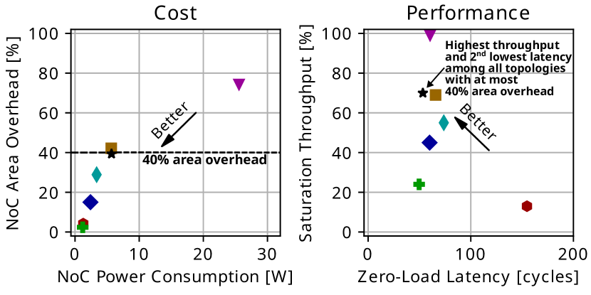
We apply our customization strategy to all four scenarios explained in the previous paragraph. Figure 6 shows a cost and performance comparison of our customized sparse Hamming graph topologies against a series of established topologies. The topologies are compared in terms of four metrics: area overhead, power consumption, saturation throughput, and zero-load latency. As a consequence, a topology is usually not strictly better than another topology, instead, each topology reaches s certain trade-off between those four metrics. In the previous paragraph, we clearly define our design goal: Maximize the throughput and minimize the latency without exceeding an area overhead of . The sparse Hamming graph topology allows us to increase the performance by adding additional links until an area overhead of is reached. As a result, our customized sparse Hamming graph topologies deliver the highest global throughput among all topologies with an area overhead of at most while providing the second lowest latency among all topologies considered. We conclude that while there is no single topology that is superior with respect to all four metrics, the sparse Hamming graph is the only topology where the cost-performance trade-off can be adjusted based on the design goals.

VI Related Work
State-of-the-art manycore architectures [39, 40] often use ring or mesh topologies with a low router radix and a high network diameter. These topologies come at a low cost, but their performance steeply deteriorates when scaling them up from dozens to hundreds or even thousands of cores. New topologies such as Flattened Butterfly [34] or SlimNoC [26] alleviate this performance degradation by reducing the network diameter, albeit with a higher router radix and cost when scaled. Topologies such as 2D torus, folded 2D torus [32], or hypercube [33] try to fill the gap between these two groups of topologies, but they can not be customized to adjust their cost-performance trade-off. Ruche networks [41] are mesh-based networks with length-adjustable skip-links, however, the number of configurations is quite limited. Sparse Hamming graphs are a superset of Ruche networks and they provide significantly more configurations than Ruche networks. As a consequence, sparse Hamming graphs offer a more fine-grained adjustment of the cost-performance trade-off.
There are several high-level models [35, 42, 43] performing cycle-level simulations for performance predictions. High-level area and power predictions are also possible, e.g., by using Orion 2.0 [44]. However, these schemes do not consider implementation details such as link routing, hence, they suffer from limited accuracy. There are also low-level models [45, 46, 47] that generate register transfer level (RTL) descriptions of the NoC. These RTL descriptions are used for accurate performance and cost predictions. Unfortunately, RTL modeling is time-consuming, requiring many person-months to explore a few topologies. This amount of effort renders low-level models impractical for the customization of NoC topologies where one wants to quickly explore a large design space. PyOCN [48] provides a unified framework for both high-level and low-level predictions, however, even they cannot combine the low execution time of high-level models with the high accuracy of low-level models. Our prediction toolchain works at the speed of high-level models while estimating low-level details by performing approximate floorplanning and link routing.
VII Conclusion
The rising number of compute cores per chip and the fact that more and more applications are becoming bound by data movement makes scalable NoC topologies more important than ever. As high performance and low cost can not be unified, we need topologies with a customizable cost-performance trade-off.
We improve the NoC topology customization process by making three major contributions: 1) a set of NoC topology design principles that reveal how to influence the NoC’s cost and performance, 2) the customizable sparse Hamming graph topology with an adjustable cost-performance trade-off, and 3) a fast and easy-to-use toolchain for predicting the NoC’s performance and cost featuring our custom model for area, power, and link latency estimates.
We show that by applying all three contributions, one is able to achieve desired cost-performance trade-offs while outperforming established topologies in terms of cost, performance, or both.
Acknowledgements
This work was supported by the ETH Future Computing Laboratory (EFCL), financed by a donation from Huawei Technologies.
It also received funding from the European Research Council
![]() (Project PSAP,
No. 101002047) and from the European Union’s HE research
and innovation programme under the grant agreement No. 101070141 (Project GLACIATION).
We thank Timo Schneider for help with computing infrastructure at SPCL.
We thank Florian Zaruba for help in the initial stages of the project.
(Project PSAP,
No. 101002047) and from the European Union’s HE research
and innovation programme under the grant agreement No. 101070141 (Project GLACIATION).
We thank Timo Schneider for help with computing infrastructure at SPCL.
We thank Florian Zaruba for help in the initial stages of the project.
References
- [1] A. Ivanov, N. Dryden, T. Ben-Nun, S. Li, and T. Hoefler, “Data movement is all you need: A case study on optimizing transformers,” Proceedings of Machine Learning and Systems, vol. 3, pp. 711–732, 2021.
- [2] A. Lumsdaine, D. Gregor, B. Hendrickson, and J. Berry, “Challenges in parallel graph processing,” Parallel Processing Letters, vol. 17, no. 01, pp. 5–20, 2007.
- [3] M. Besta et al., “Communication-efficient jaccard similarity for high-performance distributed genome comparisons,” in IEEE IPDPS. IEEE, 2020, pp. 1122–1132.
- [4] M. Besta, M. Podstawski, L. Groner, E. Solomonik, and T. Hoefler, “To push or to pull: On reducing communication and synchronization in graph computations,” in Proceedings of the 26th International Symposium on High-Performance Parallel and Distributed Computing, 2017, pp. 93–104.
- [5] S. Sakr et al., “The future is big graphs! a community view on graph processing systems,” arXiv preprint arXiv:2012.06171, 2020.
- [6] M. Besta et al., “Slim graph: Practical lossy graph compression for approximate graph processing, storage, and analytics,” 2019.
- [7] M. Besta, F. Marending, E. Solomonik, and T. Hoefler, “Slimsell: A vectorizable graph representation for breadth-first search,” in IEEE IPDPS. IEEE, 2017, pp. 32–41.
- [8] M. Besta, A. Carigiet, K. Janda, Z. Vonarburg-Shmaria, L. Gianinazzi, and T. Hoefler, “High-performance parallel graph coloring with strong guarantees on work, depth, and quality,” in SC20: International Conference for High Performance Computing, Networking, Storage and Analysis. IEEE, 2020, pp. 1–17.
- [9] L. Gianinazzi et al., “Communication-avoiding parallel minimum cuts and connected components,” ACM SIGPLAN Notices, vol. 53, no. 1, pp. 219–232, 2018.
- [10] G. Kwasniewski et al., “Red-blue pebbling revisited: near optimal parallel matrix-matrix multiplication,” in Proceedings of the International Conference for High Performance Computing, Networking, Storage and Analysis, 2019, pp. 1–22.
- [11] ——, “On the parallel i/o optimality of linear algebra kernels: near-optimal matrix factorizations,” in Proceedings of the International Conference for High Performance Computing, Networking, Storage and Analysis, 2021, pp. 1–15.
- [12] ——, “Pebbles, graphs, and a pinch of combinatorics: Towards tight i/o lower bounds for statically analyzable programs,” ACM SPAA, 2021.
- [13] M. Besta et al., “Sisa: Set-centric instruction set architecture for graph mining on processing-in-memory systems,” arXiv preprint arXiv:2104.07582, 2021.
- [14] ——, “Graphminesuite: Enabling high-performance and programmable graph mining algorithms with set algebra,” arXiv preprint arXiv:2103.03653, 2021.
- [15] M. Besta, C. Miglioli, P. S. Labini, J. Tětek, P. Iff, R. Kanakagiri, S. Ashkboos, K. Janda, M. Podstawski, G. Kwasniewski et al., “Probgraph: High-performance and high-accuracy graph mining with probabilistic set representations,” in ACM/IEEE Supercomputing, 2022.
- [16] D. Chakrabarti and C. Faloutsos, “Graph mining: laws, tools, and case studies,” Synthesis Lectures on Data Mining and Knowledge Discovery, vol. 7, no. 1, pp. 1–207, 2012.
- [17] S. U. Rehman, A. U. Khan, and S. Fong, “Graph mining: A survey of graph mining techniques,” in Seventh International Conference on Digital Information Management (ICDIM 2012). IEEE, 2012, pp. 88–92.
- [18] T. Ramraj and R. Prabhakar, “Frequent subgraph mining algorithms-a survey,” Procedia Computer Science, vol. 47, pp. 197–204, 2015.
- [19] L. Gianinazzi, M. Besta, Y. Schaffner, and T. Hoefler, “Parallel algorithms for finding large cliques in sparse graphs,” 2021.
- [20] M. Besta, R. Grob, C. Miglioli, N. Bernold, G. Kwasniewski, G. Gjini, R. Kanakagiri, S. Ashkboos, L. Gianinazzi, N. Dryden et al., “Motif prediction with graph neural networks,” in ACM KDD, 2022.
- [21] M. Besta and T. Hoefler, “Parallel and distributed graph neural networks: An in-depth concurrency analysis,” arXiv preprint arXiv:2205.09702, 2022.
- [22] T. N. Kipf and M. Welling, “Semi-supervised classification with graph convolutional networks,” arXiv preprint arXiv:1609.02907, 2016.
- [23] M. Besta, P. Iff, F. Scheidl, K. Osawa, N. Dryden, M. Podstawski, T. Chen, and T. Hoefler, “Neural graph databases,” arXiv preprint arXiv:2209.09732, 2022.
- [24] J. Zhou, G. Cui, S. Hu, Z. Zhang, C. Yang, Z. Liu, L. Wang, C. Li, and M. Sun, “Graph neural networks: A review of methods and applications,” AI Open, vol. 1, pp. 57–81, 2020.
- [25] Z. Wu, S. Pan, F. Chen, G. Long, C. Zhang, and S. Y. Philip, “A comprehensive survey on graph neural networks,” IEEE transactions on neural networks and learning systems, vol. 32, no. 1, pp. 4–24, 2020.
- [26] M. Besta, S. M. Hassan, S. Yalamanchili, R. Ausavarungnirun, O. Mutlu, and T. Hoefler, “Slim noc: A low-diameter on-chip network topology for high energy efficiency and scalability,” ACM SIGPLAN Notices, vol. 53, no. 2, pp. 43–55, 2018.
- [27] D. Bertozzi, A. Jalabert, S. Murali, R. Tamhankar, S. Stergiou, L. Benini, and G. De Micheli, “Noc synthesis flow for customized domain specific multiprocessor systems-on-chip,” IEEE transactions on parallel and distributed systems, vol. 16, no. 2, pp. 113–129, 2005.
- [28] D. Bertozzi and L. Benini, “Xpipes: A network-on-chip architecture for gigascale systems-on-chip,” IEEE circuits and systems magazine, vol. 4, no. 2, pp. 18–31, 2004.
- [29] A. Kurth, W. Rönninger, T. Benz, M. Cavalcante, F. Schuiki, F. Zaruba, and L. Benini, “An open-source platform for high-performance non-coherent on-chip communication,” IEEE Transactions on Computers, vol. 71, no. 8, pp. 1794–1809, 2021.
- [30] N. H. Weste and K. Eshraghian, Principles of CMOS VLSI design: a systems perspective. Addison-Wesley Longman Publishing Co., Inc., 1985.
- [31] W. J. Dally and B. P. Towles, Principles and practices of interconnection networks. Elsevier, 2004.
- [32] P.-H. Pham, P. Mau, and C. Kim, “A 64-pe folded-torus intra-chip communication fabric for guaranteed throughput in network-on-chip based applications,” in 2009 IEEE Custom Integrated Circuits Conference. IEEE, 2009, pp. 645–648.
- [33] A. Sahba and J. J. Prevost, “Hypercube based clusters in cloud computing,” in 2016 World Automation Congress (WAC). IEEE, 2016, pp. 1–6.
- [34] J. Kim, J. Balfour, and W. Dally, “Flattened butterfly topology for on-chip networks,” in 40th Annual IEEE/ACM International Symposium on Microarchitecture (MICRO 2007). IEEE, 2007, pp. 172–182.
- [35] N. Jiang, D. U. Becker, G. Michelogiannakis, J. Balfour, B. Towles, D. E. Shaw, J. Kim, and W. J. Dally, “A detailed and flexible cycle-accurate network-on-chip simulator,” in 2013 IEEE international symposium on performance analysis of systems and software (ISPASS). IEEE, 2013, pp. 86–96.
- [36] P. Kramer, J. Van Leeuwen et al., “Wire routing in np-complete,” 1982.
- [37] M. Cavalcante, S. Riedel, A. Pullini, and L. Benini, “Mempool: A shared-l1 memory many-core cluster with a low-latency interconnect,” in 2021 Design, Automation & Test in Europe Conference & Exhibition (DATE). IEEE, 2021, pp. 701–706.
- [38] “Amba axi and ace protocol specification,” 2021. [Online]. Available: https://developer.arm.com/documentation/ihi0022/hc/?lang=en
- [39] A. Sodani, R. Gramunt, J. Corbal, H.-S. Kim, K. Vinod, S. Chinthamani, S. Hutsell, R. Agarwal, and Y.-C. Liu, “Knights Landing: Second-generation Intel Xeon Phi product,” Ieee micro, vol. 36, no. 2, pp. 34–46, 2016.
- [40] R. Sugumar, M. Shah, and R. Ramirez, “Marvell thunderx3: Next-generation arm-based server processor,” IEEE Micro, vol. 41, no. 2, pp. 15–21, 2021.
- [41] D. C. Jung, S. Davidson, C. Zhao, D. Richmond, and M. B. Taylor, “Ruche networks: Wire-maximal, no-fuss nocs: Special session paper,” in 2020 14th IEEE/ACM International Symposium on Networks-on-Chip (NOCS). IEEE, 2020, pp. 1–8.
- [42] P. Abad, P. Prieto, L. G. Menezo, V. Puente, J.-Á. Gregorio et al., “Topaz: An open-source interconnection network simulator for chip multiprocessors and supercomputers,” in 2012 IEEE/ACM Sixth International Symposium on Networks-on-Chip. IEEE, 2012, pp. 99–106.
- [43] N. Agarwal, T. Krishna, L.-S. Peh, and N. K. Jha, “Garnet: A detailed on-chip network model inside a full-system simulator,” in 2009 IEEE international symposium on performance analysis of systems and software. IEEE, 2009, pp. 33–42.
- [44] A. B. Kahng, B. Li, L.-S. Peh, and K. Samadi, “Orion 2.0: A fast and accurate noc power and area model for early-stage design space exploration,” in 2009 Design, Automation & Test in Europe Conference & Exhibition. IEEE, 2009, pp. 423–428.
- [45] H. Kwon and T. Krishna, “Opensmart: Single-cycle multi-hop noc generator in bsv and chisel,” in 2017 IEEE International Symposium on Performance Analysis of Systems and Software (ISPASS). IEEE, 2017, pp. 195–204.
- [46] J. Chan and S. Parameswaran, “Nocgen: A template based reuse methodology for networks on chip architecture,” in 17th International Conference on VLSI Design. Proceedings. IEEE, 2004, pp. 717–720.
- [47] M. K. Papamichael and J. C. Hoe, “Connect: Re-examining conventional wisdom for designing nocs in the context of fpgas,” in Proceedings of the ACM/SIGDA international symposium on Field Programmable Gate Arrays, 2012, pp. 37–46.
- [48] C. Tan, Y. Ou, S. Jiang, P. Pan, C. Torng, S. Agwa, and C. Batten, “Pyocn: A unified framework for modeling, testing, and evaluating on-chip networks,” in 2019 IEEE 37th International Conference on Computer Design (ICCD). IEEE, 2019, pp. 437–445.