Electrical control of uniformity in quantum dot devices
Abstract
Highly uniform quantum systems are essential for the practical implementation of scalable quantum processors. While quantum dot spin qubits based on semiconductor technology are a promising platform for large-scale quantum computing, their small size makes them particularly sensitive to their local environment. Here, we present a method to electrically obtain a high degree of uniformity in the intrinsic potential landscape using hysteretic shifts of the gate voltage characteristics. We demonstrate the tuning of pinch-off voltages in quantum dot devices over hundreds of millivolts that then remain stable at least for hours. Applying our method, we homogenize the pinch-off voltages of the plunger gates in a linear array for four quantum dots reducing the spread in pinch-off voltage by one order of magnitude. This work provides a new tool for the tuning of quantum dot devices and offers new perspectives for the implementation of scalable spin qubit arrays.
Spin qubits in semiconductor quantum dots are a promising platform for quantum information processing [1, 2, 3, 4]. Group IV semiconductors such as silicon and germanium can be isotopically purified [5], enabling long quantum coherence [6, 7], high-fidelity single-qubit [8, 9, 10] and two-qubit gates [11, 12, 13] as well as multi-qubit operation [14, 15]. Spin qubits can be operated at comparatively high temperatures [16, 17, 18] and their compatibility with semiconductor technologies spurred the realization of qubits made in industrial foundries [19, 20]. However, implementing more than a few qubits on a single chip remains extremely challenging.
Variations, in particular at the nanoscale, may lead to significant alterations of the relevant device metrics [1, 2, 21], such as the voltage needed to load a single electron to be used as a spin qubit. These variations can complicate the tuning of initialization, control or readout and potentially form a roadblock for larger systems. Additionally, qubit-to-qubit variability may require the use of individual control electronics for each qubit, as is common practice in current experimental implementations, thus challenging the scalability. While several proposals have been put forward to scale quantum dot qubits [22, 2, 23, 24], in all cases a high level of device uniformity is critical in their realization.
For semiconductor quantum dot qubits, the uniformity of the potential landscape is the key parameter that dictates the number of control voltages required per qubit. Ideally, a few voltages would suffice to induce a highly regular potential landscape as drawn in Fig. 1.b. Yet, potential fluctuations are naturally present as illustrated in Fig. 1.c. They can be caused by defects and charge traps, mechanical stress induced by the deposition of metallic gates [25, 26], as well as variations in material growth or in the exact shape of the gates. The development of devices based on quantum wells buried in heterostructures, similar to that sketched in Fig. 1.a, already has led to a drastic improvement of the uniformity compared to metal-oxide-semiconductor systems [27]. This has enabled the control of up to 16 quantum dots in a four-by-four array with shared gate control [28]. However, significant variations in the quantum dot potential landscape are still commonly observed [29, 30, 28]. This raises the question whether material [4] and fabrication development [31, 32, 20, 28] will suffice to reach the required uniformity to operate large qubit arrays.
Here, we present an alternative method and demonstrate electrical control of quantum dot uniformity. Our approach takes advantage of the gate voltage hysteresis, an ubiquitous effect observed in semiconductor heterostructures, that is mostly considered as a limitation in the tune-up of quantum dots. It manifests in shifts of the gate voltage characteristics and is commonly explained by a build up of charges at the interface between the semiconductor barrier and the dielectrics which then alter the electric field in the buried quantum well [33, 34, 35, 36, 37, 38, 39]. We unveil the hysteresis and its effects on the potential landscape beneath the gates by studying how pinch-off characteristics evolve with the application of tailored stress voltage sequences. This method allows us to tune those pinch-off voltages over hundreds of millivolts after which they remain stable at least on the time scale of hours. We then apply our findings to homogeneize the plunger gate pinch-off characteristics in a linear quantum dot array reducing potential fluctuations in the quantum well underneath the corresponding gates.
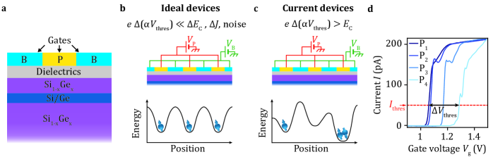
The gate voltage required to confine a single electron or hole typically varies between quantum dots in an array as it is dependent on the local electrostatic environment. These fluctuations also affect the pinch-off curve as exemplary depicted for sweeping the four plunger gates of a linear quantum dot device (similar to that shown in Fig 4.a) in Fig. 1.d. The curves reveal the local depletion of a conducting path through the quantum well and experimentally can be obtained in a very short time compared to the time required for the formation of a well defined quantum dot. Therefore, we will employ pinch-off characteristics in the following to efficiently estimate variations in the potential landscape on the length scale of single quantum dots. In particular, we focus on the pinch-off voltages defined as the gate voltages at which a current of 50 pA is reached for an applied source drain bias of V.
We study devices in 28Si/SiGe heterostructures [40] and investigate how the pinch-off voltage of a single gate evolves depending on the previously applied gate voltages. To that end, we conduct systematic transport measurements at 4.2 K similar to sequences in [41, 42, 43, 44] following the procedure depicted in Fig. 2.a. First a stress voltage is applied to the gate under study for a time min. Then the gate-voltage is swept back until the pinch-off condition is met. This sequence is repeated several times with evolving stress voltages to measure the evolution of as a function of . First, the applied stress voltage is decreased step-wise to be increased gradually again (not illustrated) after reaching a reversal point .
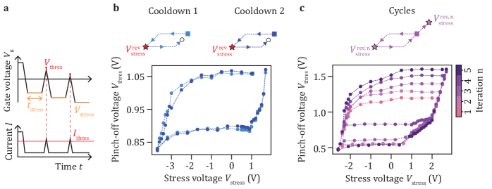
Fig. 2.b shows the resulting pinch-off voltage evolution for a plunger gate that is part of a linear quantum dot array for two different cooldowns (light blue and dark blue curve, respectively). In these cases, is first lowered step-wise from V to V. We observe that up to V the pinch-off voltages stay within mV of the first pinch-off voltage V forming a plateau. Then, they drop down rapidly to V. At V, the sweep direction is reversed and we start to increase progressively. However, we do not observe a reversed behavior. Instead, from V to V, the pinch-off voltages increase by less than mV forming a second plateau. Only when for the first(second) cooldown, starts to increase steeply again. The ensembles of (,) values draw typical hysteresis cycles with plateaus marking the ranges of applicable gate voltages over which the pinch-off voltage is not significantly changing. Furthermore, Fig. 2.b highlights the effect of thermal cycling on these measurements and reveals a remarkable overlap of the hysteresis cycles measured during two different cooldowns. A high degree of similarity is also observed when comparing successive measurements performed using the same stress voltage sequence as shown in supplementary Fig. S2 for gate S of device D. This suggests that the underlying process has a deterministic nature.
Similar experiments performed on another sample with varying reversal points result in the cycles plotted in Fig. 2.c. The shape of the curves is nearly identical for each iteration. Again, we observe plateaus where the pinch-off voltage deviates by less than mV from its first value. Yet, the position of the plateaus varies with the chosen . The pinch-off voltage plateaus can be shifted by up to mV for the lower plateau and by up to mV for the upper one. Overall, Fig. 2.b and Fig. 2.c suggest that by applying a dedicated voltage sequence the pinch-off voltage can be adjusted on-demand to chosen targets and thus that the intrinsic potential landscape underneath the gates can be tuned.
We also note that similar hysteretic behaviours, with sample-dependent variations of the exact shape of the (,) curves, are consistently found in several Si/SiGe devices (e.g. device D gate S shown in supplementary Fig. S2) as well as in samples made from Ge/SiGe heterostructures (see supplementary Fig. S3) suggesting a common underlying mechanism. The observed reproducibility and the large control window of the pinch-off voltage are the foundations of our approach to homogenize the potential landscape below an ensemble of gates.
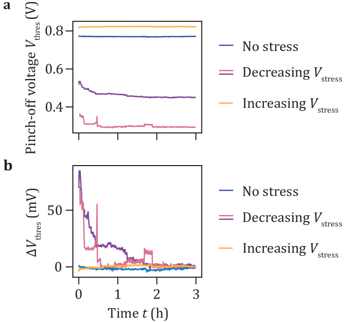
However, the electrical tuning of the intrinsic potential uniformity is of practical interest only if the resulting potential landscape remains stable afterwards. Therefore, we study how the pinch-off voltage evolves in time after stopping the hysteresis measurement cycle at varying points (see supplementary section I.C for the detailed experimental procedure). Fig. 3.a shows the time evolution directly after the application of decreasing (pink/violet) and increasing (orange) stress voltages. For comparison, we also plot how the pinch-off voltage evolves right after a cooldown without prior application of a stress voltage sequence (blue). For decreasing sequences, the pinch-off voltages converge into steady states after initial decays and the time evolution exhibits random abrupt jumps. For the situation where no stress voltage or increasing stress voltages are applied no significant variations of are observed. The relative evolution depicted in Fig. 3.b reveals that for hours, the voltage fluctuations are similar for all three situations. This is confirmed by extracting the standard deviations of for experiments with and without application of stress voltage sequence which are mV (orange), mV (pink and violet) and mV (blue), respectively. These experiments suggest that after a potential initial transient regime there is no change in the stability of the device due to the electrical tuning. This stability is observed for at least one hour and up to three depending on the voltage sequence applied.
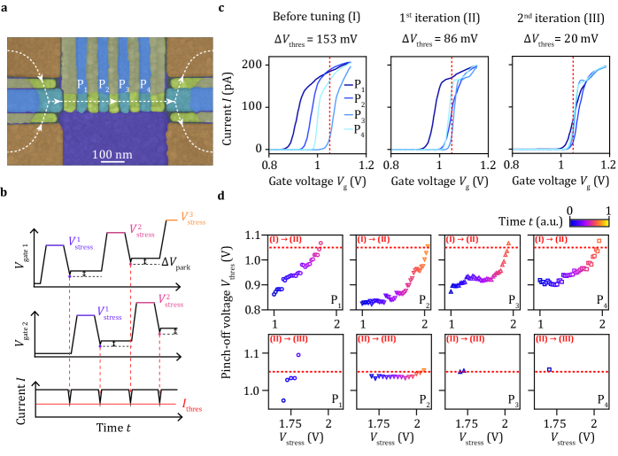
Next we apply our findings and probe the capability to homogenize the pinch-off voltages of a group of plunger gates with i in [1,4] in a quantum dot array. Fig 4.a displays the device studied which has a geometry similar to linear quantum dot arrays in ref. [29, 45, 12, 15]. The pinch-off characteristics recorded prioir to the tuning sequence are depicted in the left panel of Fig 4.c and show a spread of 153 mV. Employing increasing gate voltage stress we tune the individual plunger pinch-off voltages to a target value V chosen before starting the tuning. Fig. 4.b illustrates the procedure followed for the specific case of two gates. is gradually increased in steps n. For each , the plunger gates are sequentially stressed, measured and parked mV above their latest pinch-off voltage where they remain until the next stress voltage is selected. When a pinch-off voltage crosses the target voltage the corresponding plunger gate is henceforth not stressed anymore. A full automated round of this sequence finishes after all pinch-off voltages are larger than the target voltage. The complete procedure is repeated two times with a stress voltage resolution of mV taking approximately 9 hours in total. All applied stress voltages and measured pinch-off voltages are visualized in the panels of Fig. 4.d. After each repetition a pinch-off characterization is performed with the resulting curves depicted in Fig. 4.c. During the first round the pinch-off voltages shift towards the target voltage (indicated by the red dashed line) finally spreading in a range of mV around it. This spread is further reduced by the following iteration reaching a final value of mV. Afterwards the plunger pinch-off characteristics are observed to remain stable at least for 20 minutes (see supplementary Fig. S4).
To put this result into context, we compare the final spread of pinch-off voltages to the degree of uniformity needed to load an array of quantum dots with a single electron at each site using a single common gate voltage. This would require the potential fluctuations below the gates to be smaller than the average charging voltage that is needed to alter the charge occupation, with the charging energy and the gate lever arm. This charging voltage typically ranges from 10 to 60 mV in devices similar to that under study [29, 45, 27, 46]. Assuming that pinch-off voltages constitute a witness of the intrinsic potential landscape in the quantum well, the final spread mV reached after electrical tuning promises a path towards the homogenization of quantum dot potentials inside an array. Even smaller spreads might be achievable by decreasing the stress voltage resolution . We envision that a similar method could be used to tune the potential underneath all plunger and all barrier gates simultaneously. It could allow to also equalize the inter-dot tunnel couplings and to reach an energy landscape similar to that in Fig. 1.b.
At the same time, optimization of the automated procedure could lead to a significant increase of the tuning efficiency. Such an optimized procedure may be obtained by dividing the tuning into coarse and fine steps and exploring different stressing times and thereby could drastically reduce the tuning time. Additionally, utilizing a model to predict the effect of the next stress voltage, could further minimize the number of steps required to reach the target potentials and simultaneous tuning of multiple gates may be envisioned in larger quantum dot arrays.
Adapted tuning procedures may also be designed for scalable device architectures. In a crossbar gate architecture [24, 28], one could envision to apply different stressing voltages on different sets of gates such that only close to the crossing points of these gates the combined electric field is strong enough to shift the intrinsic potential. This would allow parallel but individual stressing of selected sites in a row-by-row manner. Another degree of selectivity might be provided through biasing of purposely isolated parts of the quantum well. Effectively, this would locally change the gates’ reference potential and thereby locally alter the effect of the stressing voltages applied to them. Further work is needed to confirm the viability of these approaches.
Also, a better understanding of the underlying mechanism of the hysteresis would be valuable to exploit it most efficiently. A possible origin might be the trapping and detrapping of charge in or close to the dielectric capping layer caused by the application of stress voltages [33, 34, 35, 36, 37, 38]. For example, a positive stress voltage might enable the tunnelling of electrons from the quantum well or traps underneath non-stressed gates to traps underneath the stressed gate. These traps could be bound states in the non-oxidized part of the silicon capping layer or at its SiGe interface. They can be induced by charge defects in the gate oxide [47] or emerge due to mechanical stress originating from the deposition of metallic gates [25, 26]. Also, charge trapping into and out of of unpassivated silicon and germanium dangling bonds [48, 49, 50], charge trapping in the oxide itself mediated by leakage currents [51, 52, 53, 44] or movement of mobile ions [54] might be underlying the hysteresis. In all cases, when the gate voltage stress is removed the charges would be expected to be immobile at the device operation temperature and would cause local shifts in the intrinsic potential landscape observable as alterations in the pinch-off characteristics. This tunneling and trapping of charge also would be highly similar to the principle used to operate modern flash memories (based on electrically erasable programmable read only memories) which encode their stored information in pinch-off voltages and rely on gate stacks specifically engineered for that purpose [55, 53]. They could inspire new heterostructures and gate stacks with dedicated trapping layers further refining the tunability of the potential landscape using the gate voltage hysteresis.
In conclusion, we have presented a new method to increase the electrostatic potential uniformity in quantum dot devices electrically. We show that we can take advantage of hysteric shifts in gate voltage characteristics to deliberately tune pinch-off voltages across a wide range of more than 500 mV by applying stress voltage sequences. The resulting states remain stable on the time scale of hours. Utilizing our method, we have shifted and equalized the pinch-off voltages of four plunger gates in a linear quantum dot array to a predetermined target voltage. Although most of our results were obtained in Si/SiGe heterostructures other measurements indicate that the effect and method also can be used in other heterostructure materials like Ge/SiGe. Our work opens up a new path to increase uniformity in quantum dot based spin qubits. It may enable reducing overheads in tuning and control making the implementation of scalable architectures more feasible in practise.
Data availability
The data and analysis supporting this work are openly available in a public Zenodo repository at https://doi.org/10.5281/zenodo.7225478 [56].
Acknowledgements
We gratefully acknowledge D. Michalak, D. Degli-Esposti, M. Mehmandoost for sharing their expertise, their insights on the underlying physics and for their valuable advices. We also acknowledge S. Philips for his help on the Si/SiGe device designing. We thank L.M.K Vandersypen for his feedback as well as all the members of the Veldhorst and Vandersypen group for stimulating discussions. We thank J. D. Mensingh and N. P. Alberts for their technical support with the experimental set-ups and S. L. de Snoo for software support.
We acknowledge support through an ERC Starting Grant and through an NWO projectruimte. This research was supported by the European Union’s Horizon 2020 research and innovation programme under the Grant Agreement No. 951852 (QLSI project). Research was sponsored by the Army Research Office (ARO) and was accomplished under Grant No. W911NF-17-1-0274. The views and conclusions contained in this document are those of the authors and should not be interpreted as representing the official policies, either expressed or implied, of the Army Research Office (ARO), or the U.S. Government. The U.S. Government is authorized to reproduce and distribute reprints for Government purposes notwithstanding any copyright notation herein.
Competing interest
The authors declare no competing financial interest.
References
- Zwanenburg et al. [2013] F. A. Zwanenburg, A. S. Dzurak, A. Morello, M. Y. Simmons, L. C. L. Hollenberg, G. Klimeck, S. Rogge, S. N. Coppersmith, and M. A. Eriksson, Silicon quantum electronics, Rev. Mod. Phys. 85, 961 (2013).
- Vandersypen et al. [2017] L. M. K. Vandersypen, H. Bluhm, J. S. Clarke, A. S. Dzurak, R. Ishihara, A. Morello, D. J. Reilly, L. R. Schreiber, and M. Veldhorst, Interfacing spin qubits in quantum dots and donors - hot, dense, and coherent, npj Quantum Inf 3, 34 (2017).
- Scappucci et al. [2021a] G. Scappucci, C. Kloeffel, F. A. Zwanenburg, D. Loss, M. Myronov, J.-J. Zhang, S. De Franceschi, G. Katsaros, and M. Veldhorst, The germanium quantum information route, Nature Reviews Materials 6, 926 (2021a).
- Scappucci et al. [2021b] G. Scappucci, P. J. Taylor, J. R. Williams, T. Ginley, and S. Law, Crystalline materials for quantum computing: Semiconductor heterostructures and topological insulators exemplars, MRS Bulletin 46, 596 (2021b).
- Itoh and Watanabe [2014] K. M. Itoh and H. Watanabe, Isotope engineering of silicon and diamond for quantum computing and sensing applications, MRS Communications 4, 143–157 (2014).
- Veldhorst et al. [2014] M. Veldhorst, J. C. C. Hwang, C. H. Yang, A. W. Leenstra, B. de Ronde, J. P. Dehollain, J. T. Muhonen, F. E. Hudson, K. M. Itoh, A. Morello, and A. S. Dzurak, An addressable quantum dot qubit with fault-tolerant control-fidelity, Nature Nanotechnology 9, 941 (2014).
- Stano and Loss [2021] P. Stano and D. Loss, Review of performance metrics of spin qubits in gated semiconducting nanostructures, arXiv , 2107.06485 (2021).
- Dehollain et al. [2016] J. P. Dehollain, J. T. Muhonen, R. Blume-Kohout, K. M. Rudinger, J. King Gamble, E. Nielsen, A. Laucht, S. Simmons, R. Kalra, A. S. Dzurak, and A. Morello, Optimization of a solid-state electron spin qubit using gate set tomography, New J. Phys. 18, 103018 (2016).
- Yoneda et al. [2018] J. Yoneda, K. Takeda, T. Otsuka, T. Nakajima, , M. R. Delbecq, G. Allison, T. Honda, T. Kodera, S. Oda, Y. Hoshi, U. Noritaka, K. M. Itoh, and S. Tarucha, A quantum-dot spin qubit with coherence limited by charge noise and fidelity higher than 99.9%, Nature Nanotechnology 13, 102 (2018).
- Lawrie et al. [2021] W. I. L. Lawrie, M. Russ, F. van Riggelen, N. W. Hendrickx, S. L. de Snoo, A. Sammak, L. M. K. Vandersypen, G. Scappucci, and M. Veldhorst, Simultaneous driving of semiconductor spin qubits at the fault-tolerant threshold, arXiv , 2109.07837 (2021).
- Mądzik et al. [2022] M. Mądzik, S. Asaad, A. Youssry, B. Joecker, K. M. Rudinger, E. Nielsen, K. C. Young, T. J. Proctor, A. D. Baczewski, A. Laucht, V. Schmitt, F. E. Hudson, K. M. Itoh, A. M. Jakob, B. C. Johnson, D. N. Jamieson, A. S. Dzurak, C. Ferrie, R. Blume-Kohout, and A. Morello, Precision tomography of a three-qubit donor quantum processor in silicon, Nature 601, 348 (2022).
- Noiri et al. [2022] A. Noiri, K. Takeda, T. Nakajima, T. Kobayashi, A. Sammak, G. Scappucci, and S. Tarucha, Fast universal quantum gate above the fault-tolerance threshold in silicon, Nature 601, 338 (2022).
- Xue et al. [2022] X. Xue, M. Russ, N. Samkharadze, B. Undseth, A. Sammak, G. Scappucci, and L. M. K. Vandersypen, Quantum logic with spin qubits crossing the surface code threshold, Nature 601, 343 (2022).
- Hendrickx et al. [2021] N. W. Hendrickx, W. I. L. Lawrie, M. Russ, F. van Riggelen, S. L. de Snoo, R. N. Schouten, A. Sammak, G. Scappucci, and M. Veldhorst, A four-qubit germanium quantum processor, Nature 591, 580 (2021).
- Philips et al. [2022] S. G. J. Philips, M. T. Mądzik, S. V. Amitonov, S. L. de Snoo, M. Russ, N. Kalhor, C. Volk, W. I. L. Lawrie, D. Brousse, L. Tryputen, B. Paquelet Wuetz, A. Sammak, M. Veldhorst, G. Scappucci, and L. M. K. Vandersypen, Universal control of a six-qubit quantum processor in silicon, Nature 609, 919–924 (2022).
- Petit et al. [2020] L. Petit, H. G. J. Eenink, M. Russ, W. I. L. Lawrie, N. W. Hendrickx, S. G. J. Phillips, J. S. Clarke, L. M. K. Vandersypen, and M. Veldhorst, Universal quantum logic in hot silicon qubits, Nature 580, 355 (2020).
- Yang et al. [2020] C. H. Yang, R. C. C. Leon, J. C. C. Hwang, A. Saraiva, T. Tanttu, W. Huang, J. Camirand Lemyre, K. W. Chan, K. Y. Tan, F. E. Hudson, K. M. Itoh, A. Morello, M. Pioro-Ladrière, A. Laucht, and A. S. Dzurak, Operation of a silicon quantum processor unit cell above one kelvin, Nature 580, 350 (2020).
- Camenzind et al. [2022] L. C. Camenzind, S. Geyer, A. Fuhrer, R. J. Warburton, D. M. Zumbühl, and A. Kuhlmann, A hole spin qubit in a fin field-effect transistor above 4 kelvin, Nature Electronics 5, 178 (2022).
- Ansaloni et al. [2020] F. Ansaloni, A. Chatterjee, H. Bohuslavskyi, B. Bertrand, L. Hutin, M. Vinet, and F. Kuemmeth, Single-electron operations in a foundry-fabricated array of quantum dots, Nature Communications 11, 6399 (2020).
- Zwerver et al. [2022] A.-M. J. Zwerver, T. Krähenmann, T. F. Watson, L. Lampert, H. C. George, R. Pillarisetty, S. A. Bojarski, P. Amin, S. V. Amitonov, J. M. Boter, R. Caudillo, D. Corras-Serrano, J. P. Dehollain, G. Droulers, E. M. Henry, R. Kotlyar, M. Lodari, F. Lüthi, D. J. Michalak, B. K. Mueller, S. Neyens, J. Roberts, N. Samkharadze, G. Zheng, O. K. Zietz, G. Scappucci, M. Veldhorst, L. M. K. Vandersypen, and J. S. Clarke, Qubits made by advanced semiconductor manufacturing, Nature Electronics 5, 184 (2022).
- Bavdaz et al. [2022] P. L. Bavdaz, H. G. J. Eenink, J. van Staveren, M. Lodari, C. G. Almudever, J. S. Clarke, F. Sebasatiano, M. Veldhorst, and G. Scappucci, A quantum dot crossbar with sublinear scaling of interconnects at cryogenic temperature, npj Quantum Information 8, 86 (2022).
- Hill et al. [2015] C. D. Hill, E. Peretz, S. J. Hile, M. G. House, M. Fuechsle, S. Rogge, M. Y. Simmons, and L. C. L. Hollenberg, A surface code quantum computer in silicon, Science Advances 1, e1500707 (2015).
- Veldhorst et al. [2017] M. Veldhorst, H. G. J. Eenink, C. H. Yang, and A. S. Dzurak, Silicon CMOS architecture for a spin-based quantum computer, Nature Communications 8, 1766 (2017).
- Li et al. [2018] R. Li, L. Petit, D. P. Franke, J. P. Dehollain, J. Helsen, M. Steudtner, N. K. Thomas, Z. R. Yoscovits, K. J. Singh, S. Wehner, L. M. K. Vandersypen, J. Clarke, and M. Veldhorst, A crossbar network for silicon quantum dot qubits, Science Advances 4, eaar3960 (2018).
- Thorbeck and Zimmerman [2015] T. Thorbeck and N. M. Zimmerman, Formation of strain-induced quantum dots in gated semiconductor nanostructures, AIP Advances 5, 087107 (2015).
- Stein et al. [2021] R. M. Stein, Z. S. Barcikowski, S. J. Pookpanratana, J. M. Pomeroy, and M. D. Stewart Jr., Alternatives to aluminum gates for silicon quantum devices: Defects and strain, Journal of Applied Physics 130, 115102 (2021).
- Lawrie et al. [2020] W. I. L. Lawrie, H. G. J. Eenink, N. W. Hendrickx, J. M. Boter, L. Petit, S. V. Amitonov, M. Lodari, B. Paquelet Wuetz, C. Volk, S. G. J. Philips, G. Droulers, N. Kalhor, F. van Riggelen, D. Brousse, A. Sammak, L. M. K. Vandersypen, G. Scappucci, and M. Veldhorst, Quantum dot arrays in silicon and germanium, Applied Physics Letters 116, 080501 (2020).
- Borsoi et al. [2022] F. Borsoi, N. W. Hendrickx, V. John, S. Motz, F. van Riggelen, A. Sammak, S. L. de Snoo, G. Scappucci, and M. Veldhorst, Shared control of a 16 semiconductor quantum dot crossbar array, arXiv , 2209.06609 (2022).
- Zajac et al. [2016] D. M. Zajac, T. M. Hazard, X. Mi, E. Nielsen, and J. R. Petta, Scalable gate architecture for a one-dimensional array of semiconductor spin qubits, Physical Review Applied 6, 054013 (2016).
- Mills et al. [2019] A. R. Mills, D. M. Zajac, M. J. Gullans, F. J. Schupp, T. M. Hazard, and J. R. Petta, Shuttling a single charge across a one-dimensional array of silicon quantum dots, Nature Communications 10, 1063 (2019).
- Dodson et al. [2020] J. P. Dodson, N. Holman, B. Thorgrimsson, S. F. Neyens, E. R. MacQuarrie, T. McJunkin, R. H. Foote, L. F. Edge, S. N. Coppersmith, and M. A. Eriksson, Fabrication process and failure analysis for robust quantum dots in silicon, Nanotechnology 31, 505001 (2020).
- Ha et al. [2022] W. Ha, S. D. Ha, M. D. Choi, Y. Tang, A. E. Schmitz, M. P. Levendorf, K. Lee, J. M. Chappell, T. S. Adams, D. R. Hulbert, E. Acuna, R. S. Noah, J. W. Matten, M. P. Jura, J. A. Wright, M. T. Rakher, and M. G. Borselli, A flexible design platform for Si/SiGe exchange-only qubits with low disorder, Nano Letters 22, 1443 (2022).
- Lu et al. [2011] T. M. Lu, C.-H. Lee, S.-H. Huang, D. C. Tsui, and C. W. Liu, Upper limit of two-dimensional electron density in enhancement-mode Si/SiGe heterostructure field-effect transistors, Applied Physics Letters 99, 153510 (2011).
- Huang et al. [2014] C.-T. Huang, J.-Y. Li, K. S. Chou, and J. C. Sturm, Screening of remote charge scattering sites from the oxide/silicon interface of strained Si two-dimensional electron gases by an intermediate tunable shielding electron layer, Applied Physics Letters 104, 243510 (2014).
- Laroche et al. [2015] D. Laroche, S. H. Huang, E. Nielsen, Y. Chuang, J. Y. Li, C. W. Liu, and T. M. Lu, Scattering mechanisms in shallow undoped Si/SiGe quantum wells, AIP Advances 5, 107106 (2015).
- Su et al. [2017] Y.-H. Su, Y. Chuang, C.-Y. Liu, J.-Y. Li, and T.-M. Lu, Effects of surface tunneling of two-dimensional hole gases in undoped Ge/GeSi heterostructures, Physical Review Materials 1, 044601 (2017).
- Chou et al. [2018] K.-Y. Chou, N.-W. Hsu, Y.-H. Su, C.-T. Chou, P.-Y. Chiu, Y. Chuang, and J.-Y. Li, Temperature dependence of dc transport characteristics for a two-dimensional electron gas in an undoped Si/SiGe heterostructure, Applied Physics Letters 112, 083502 (2018).
- Su et al. [2019] Y.-H. Su, K.-Y. Chou, Y. Chuang, T.-M. Lu, and J.-Y. Li, Electron mobility enhancement in an undoped Si/SiGe heterostructure by remote carrier screening, Journal of Applied Physics 125, 235705 (2019).
- Degli Esposti et al. [2022] D. Degli Esposti, B. Paquelet Wuetz, V. Fezzi, M. Lodari, A. Sammak, and G. Scappucci, Wafer-scale low-disorder 2DEG in 28Si/SiGe without an epitaxial Si cap, Applied Physics Letters 120, 184003 (2022).
- Paquelet Wuetz et al. [2021] B. Paquelet Wuetz, M. P. Losert, S. Koelling, L. E. A. Stehouwer, A.-M. J. Zwerver, S. G. J. Philips, M. T. Mądzik, X. Xue, G. Zheng, M. Lodari, S. V. Amitonov, N. Samkharadze, A. Sammak, L. M. K. Vandersypen, R. Rahman, S. N. Coppersmith, O. Moutanabbir, M. Friesen, and G. Scappucci, Atomic fluctuations lifting the energy degeneracy in Si/SiGe quantum dots, arXiv , 2112.09606 (2021).
- Ershov et al. [2003] M. Ershov, S. Saxena, H. Karbasi, S. Winters, S. Minehane, J. Babcock, R. Lindley, P. Clifton, M. Redford, and A. Shibkov, Dynamic recovery of negative bias temperature instability in p-type metal–oxide–semiconductor field-effect transistors, Applied Physics Letters 83, 1647 (2003).
- Kaczer et al. [2008] B. Kaczer, T. Grasser, J. Roussel, J. Martin-Martinez, R. O’Connor, B. J. O’Sullivan, and G. Groeseneken, Ubiquitous relaxation in BTI stressing—new evaluation and insights, in 2008 IEEE International Reliability Physics Symposium (2008) pp. 20–27.
- Lelis et al. [2015] A. J. Lelis, R. Green, D. B. Habersat, and M. El, Basic mechanisms of threshold-voltage instability and implications for reliability testing of Sic MOSFETs, IEEE Transactions on Electron Devices 62, 316 (2015).
- Franco et al. [2014] J. Franco, A. Alian, B. Kaczer, D. Lin, T. Ivanov, A. Pourghaderi, K. Martens, Y. Mols, D. Zhou, N. Waldron, S. Sioncke, T. Kauerauf, N. Collaert, A. Thean, M. Heyns, and G. Groeseneken, Suitability of high-k gate oxides for III–V devices: A PBTI study in In0.53Ga0.47As devices with Al2O3, in 2014 IEEE International Reliability Physics Symposium (2014) pp. 6A.2.1–6A.2.6.
- Neyens et al. [2019] S. F. Neyens, E. R. MacQuarrie, J. P. Dodson, J. Corrigan, N. Holman, B. Thorgrimsson, M. Palma, T. McJunkin, L. F. Edge, M. Friesen, S. N. Coppersmith, and M. A. Eriksson, Measurements of capacitive coupling within a quadruple-quantum-dot array, Physical Review Applied 12, 064049 (2019).
- Takeda et al. [2021] K. Takeda, A. Noiri, T. Nakajima, J. Yoneda, T. Kobayashi, and S. Tarucha, Quantum tomography of an entangled three-qubit state in silicon, Nature Nanotechnology 16, 965 (2021).
- Goetzberger et al. [1968] A. Goetzberger, V. Heine, and E. H. Nicollian, Surface states in silicon from charge in the oxide coating, Applied Physics Letters 12, 95 (1968).
- Poindexter and Caplan [1988] E. H. Poindexter and P. J. Caplan, Electron spin resonance of inherent and process induced defects near the Si/SiO2 interface of oxidized silicon wafers, Journal of Vacuum Science & Technology A 6, 1352 (1988).
- Lenahan and Conley Jr. [1998] P. M. Lenahan and J. F. Conley Jr., What can electron paramagnetic resonance tell us about the Si/SiO2 system?, Journal of Vacuum Science & Technology B: Microelectronics and Nanometer Structures Processing, Measurement, and Phenomena 16, 2134 (1998).
- Stesmans et al. [2014] A. Stesmans, T. Nguyen Hoang, and V. V. Afanas’ev, Hydrogen interaction kinetics of Ge dangling bonds at the Si0.25Ge0.75/SiO2 interface, Journal of Applied Physics 116, 044501 (2014).
- Kerber et al. [2003] A. Kerber, E. Cartier, G. Groeseneken, H. E. Maes, and U. Schwalke, Stress induced charge trapping effects in SiO2/Al2O3 gate stacks with TiN electrodes, Journal of Applied Physics 94, 6627 (2003).
- Pioro-Ladrière et al. [2005] M. Pioro-Ladrière, J. H. Davies, A. R. Long, A. S. Sachrajda, L. Gaudreau, P. Zawadzki, J. Lapointe, J. Gupta, Z. Wasilewski, and S. Studenikin, Origin of switching noise in GaAsAlGa1-xAs lateral gated devices, Physical Review B 72, 115331 (2005).
- Sze and Ng [2006] S. M. Sze and K. K. Ng, Physics of Semiconductor Devices (John Wiley & Sons, 2006).
- Vanheusden et al. [1998] K. Vanheusden, W. L. Warren, D. M. Fleetwood, J. R. Schwank, M. R. Shaneyfelt, B. L. Draper, P. S. Winokur, R. A. B. Devine, L. B. Archer, G. A. Brown, and R. M. Wallace, Chemical kinetics of mobile-proton generation and annihilation in SiO2 thin films, Applied Physics Letters 73, 674 (1998).
- Hoffmann [2004] K. Hoffmann, System Integration: From Transistor Design to Large Scale Integrated Circuits (John Wiley & Sons, Incorporated, Hoboken, United Kingdom, 2004).
- Meyer et al. [2022] M. Meyer, C. Déprez, T. R. van Abswoude, D. Liu, C. Wang, S. Karwal, S. Oosterhout, F. Borsoi, A. Sammak, N. W. Hendrickx, G. Scappucci, and M. Veldhorst, Dataset underlying the manuscript: Electrical control of uniformity in quantum dot devices, Zenodo.org , 10.5281/zenodo.7225478 (2022).