Quadristor: a novel device for superconducting electronics
Abstract
We designed and experimentally demonstrated a four-terminal superconducting device which can function as a non-latching (reversible) superconducting switch from the diode regime to the resistive state by applying a control current much smaller than the main transport current. The device utilizes a vortex-based superconducting diode mechanism which is switched back and forth via the injection of flux quanta through auxiliary current leads. Various applications in superconducting electronics can be foreseen.
Simultaneous breaking of time reversal symmetry and inversion symmetry generates the superconducting diode effect [1, 2, 3, 4, 5, 6, 7, 8]. The time reversal symmetry could be broken via an externally applied magnetic field or internal inclusions of magnetic micro-clusters, while the inversion symmetry could be broken in several ways: [9, 10, 11, 12, 13, 4, 6, 14, 15, 16, 17, 18, 19, 20, 21, 22].
The recent spike of research in the area of superconducting diodes is paving a road towards the future practical application of these novel devices in superconducting electronics. Moreover, it inspires substantiated hopes that the next stages of work, in analogy with semiconductor electronics, will be accomplished by developing superconducting transistors. By a “transistor” we refer to a regulated diode, whose resistive state can be controlled by an externally applied signal exerting much less power than the one it controls. In this report, we introduce such a device. Because of the specifics of superconductivity, where the devices are current-biased, the controlling agent in our design is a current supplied by two auxiliary leads. This justifies the term “quadristor”: two leads for the transport and two leads for the control currents. Via this relatively small control current, the diode effect can be turned off and on by demand without noticeable latching effect and can function as a fast switch or as a signal controller/amplifier.
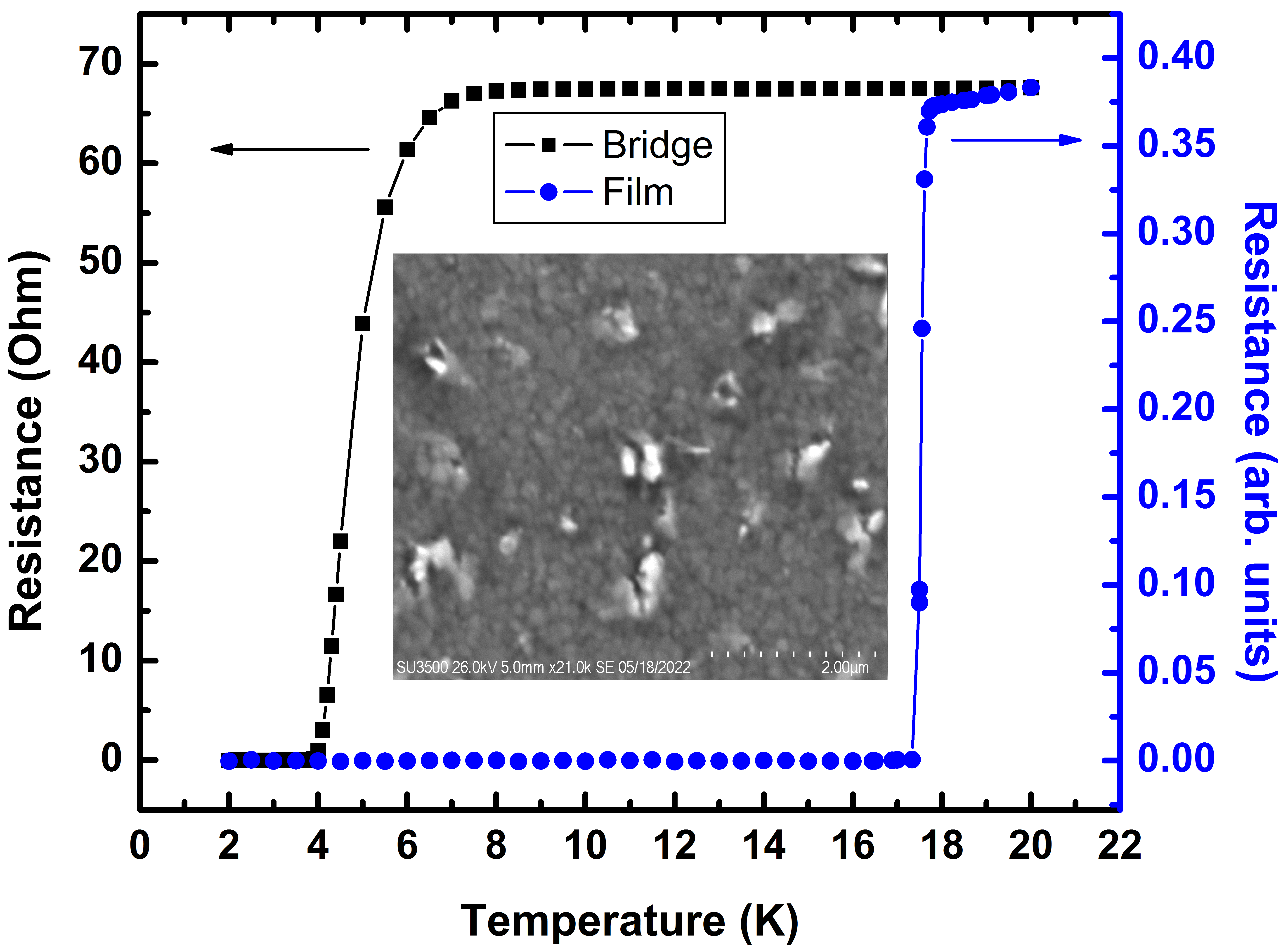
We used films on sapphire substrates with , Fig. 1.
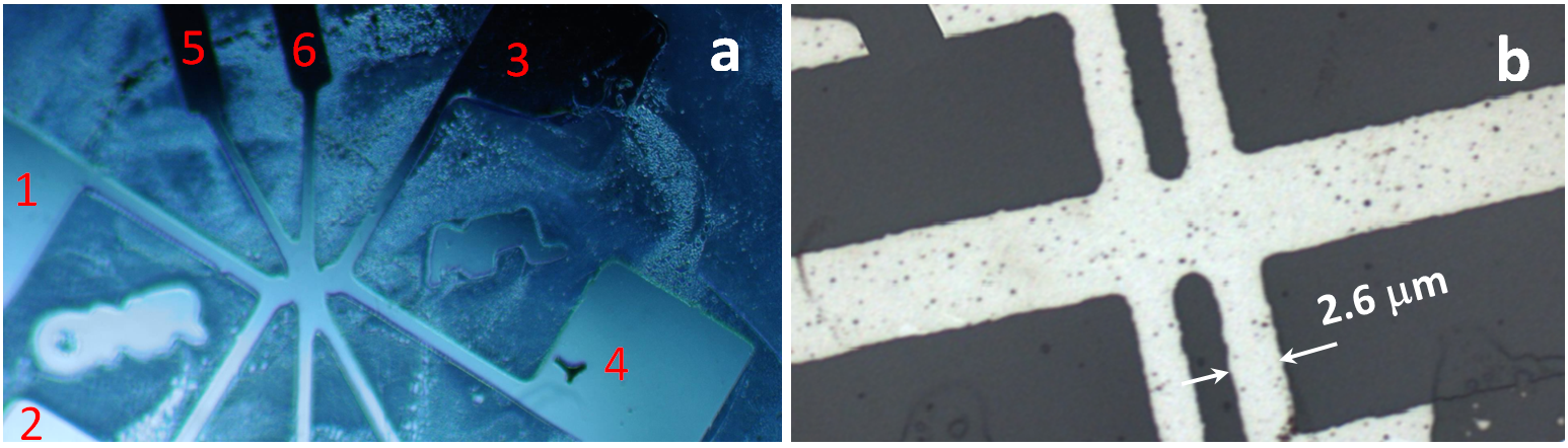
The device was fabricated by a multistage lithographic patterning process described in Fig. 2 (the details of deposition and lithography patterning are described elsewhere [22]).
Ion milling affects the physical properties of bridges and reduces the critical temperatures (see. e.g., [19, 22]). In the current case, the bridge had (Fig. 1).
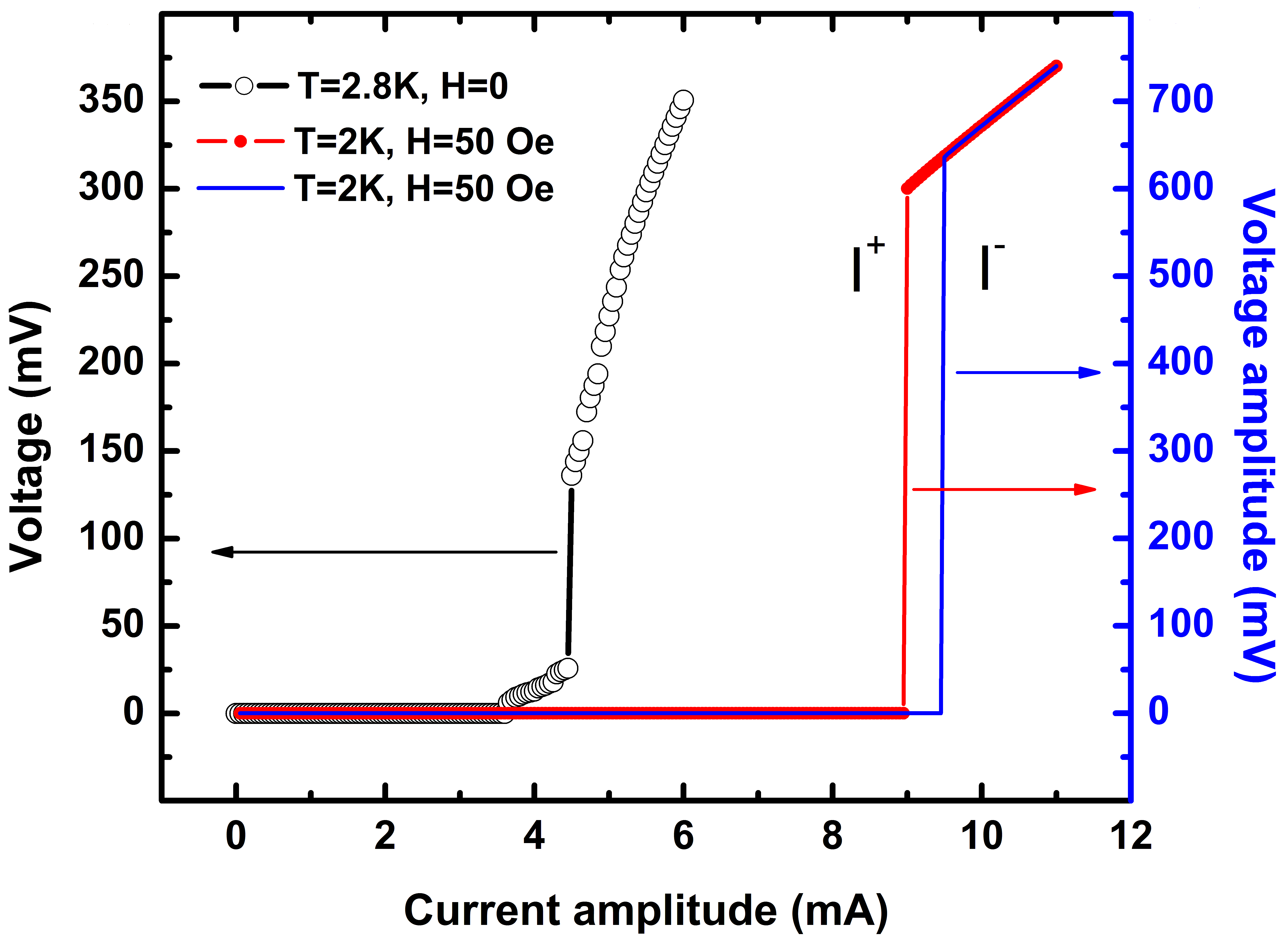
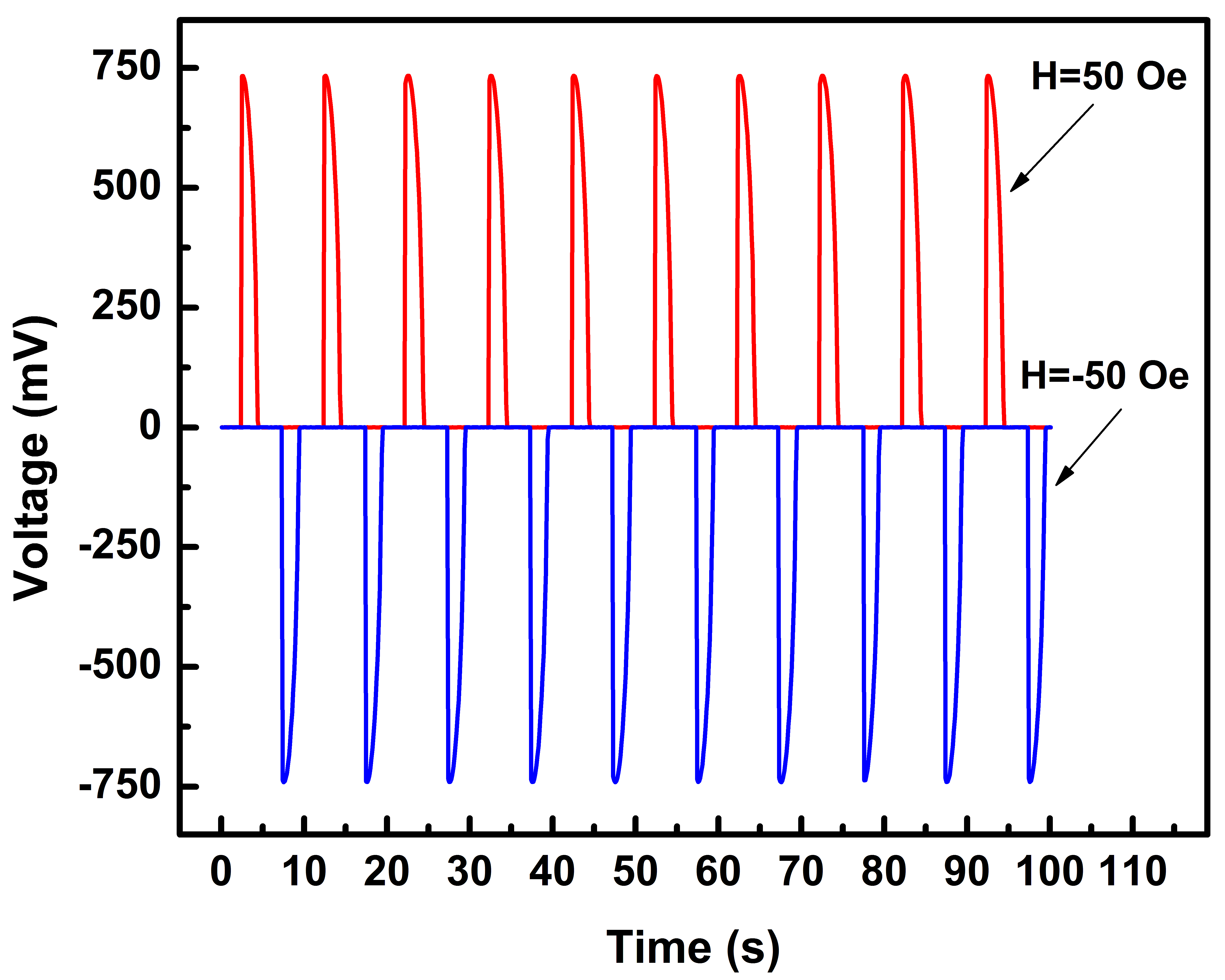
As was reported previously [22], the bridges prepared in this manner demonstrate a noticeable critical current difference . For the bridge under study, we reached at and Oe (Fig. 3; similarly with [19, 22], at positive values of applied magnetic field, and vice versa) with very robust diode effect (Fig. 4).
It is worth mentioning that the existence of nanoholes displayed in Fig. 2b creates an analogy between this diode behavior and the one mentioned in Ref. [26] where the conformally mapped holes were artificially introduced in a homogeneous superconducting strip to break the inversion symmetry. In our case, the inhomogeneously populated nanoholes exist as a consequence of photo-projection mask imperfections which are inevitable at the laser printing technique used for the mask preparation, and unexpectedly caused a positive impact. This, however, needs more studies, since, as mentioned in [19, 21, 22], the edge imperfections can also facilitate the inversion symmetry breaking.
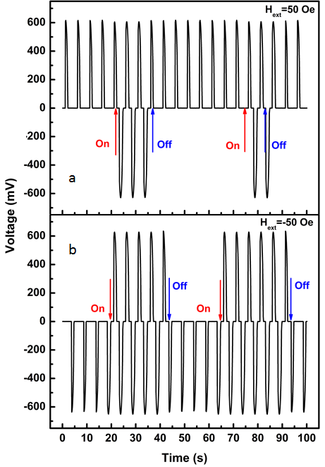
The main idea of the quadristor design stemmed from a hypothesis that the underlying mechanism of this diode effect is based on vortex lattice dynamics in the active area of the bridge. The additional leads (the pairs and ) attached to that area were added for seeding vortices in the laminar flow of supercurrent, thus triggering major vortex pattern (turbulence) generation. The intuitive belief that this external triggering should work has been indeed experimentally confirmed (Fig. 5): the diode effect via leads is replaced by a resistive state when the auxiliary current through the leads and is On (this numbering corresponds to that in Fig. 2a). The prediction that there would be no latching was much less obvious. However, the removal of the current through these auxiliary leads restored the laminar flow at diode performance, as Fig. 5 demonstrates.
Predictably, a similar result occurs when one uses the other two auxiliary leads ( and ) for the control current.
The device performance resembles that of the planar transistor-type devices suggested recently in multiple articles . However, in these devices, the design is based on different principles, for example, the field-effect, which modifies the density of states, or the injection of high-energy electrons, which generates nonequilibrium phonon fluxes, etc. These approaches require the application of potentials in the eV range, which is above the intrinsic characteristic energy scale of superconductors (meV). The controlling current of our quadristor is significantly smaller than the transport current through it, so our device can be effectively used in circuits of superconducting microelectronics, such as logical elements, amplifiers, etc.
In conclusion, we experimentally demonstrated a newly suggested design of current-controlled four-terminal device which reversibly switches the superconducting diode into a resistive state and back. The mechanism of switching is based on nonequilibrium kinetics of vortices in the active area of the device. Since the dioding is also based on this mechanism and the high-frequency operation is demonstrated for it [22], there are reasons to expect that switching will also be possible at high-frequencies.
The aim of this research was to prove the operational principle of the device. Importantly, the control current mA) is much smaller than the amplitude of the ac transport current ( mA). At further optimization of the quadristor parameters, the gain may be further enhanced. However, even with the currently achieved gain, , the quadristor can serve as a signal amplifier. Moreover, the transport current through it can be controlled by many switches (two in our current design). Thus, our development opens opportunities for various applications in true (non-hybrid) superconducting microelectronics, including logical units in leading-edge quantum information tasks. It also opens novel opportunities for exploration of fundamental problems of non-equilibrium states of superconductors and turbulent-laminar motion interplay in superfluid liquids.
This work is supported by the ONR grants N00014-21-1-2879 and N00014-20-1-2442.
References
- Tokura and Nagaosa [2018] Y. Tokura and N. Nagaosa, Nonreciprocal responses from non-centrosymmetric quantum materials, Nature Communications 9, 3740 (2018).
- Wakatsuki and Nagaosa [2018] R. Wakatsuki and N. Nagaosa, Nonreciprocal Current in Noncentrosymmetric Rashba Superconductors, Phys. Rev. Lett. 121, 026601 (2018).
- Hoshino et al. [2018] S. Hoshino, R. Wakatsuki, K. Hamamoto, and N. Nagaosa, Nonreciprocal charge transport in two-dimensional noncentrosymmetric superconductors, Phys. Rev. B 98, 054510 (2018).
- Ando et al. [2020] F. Ando, Y. Miyasaka, T. Li, J. Ishizuka, T. Arakawa, Y. Shiota, T. Moriyama, Y. Yanase, and T. Ono, Observation of superconducting diode effect, Nature 584, 373 (2020).
- Ideue and Iwasa [2020] T. Ideue and Y. Iwasa, One-way supercurrent achieved in an electrically polar film, Nature 584, 349 (2020).
- Baumgartner et al. [2022a] C. Baumgartner, L. Fuchs, A. Costa, S. Reinhardt, S. Gronin, G. C. Gardner, T. Lindemann, M. J. Manfra, P. E. Faria Junior, D. Kochan, J. Fabian, N. Paradiso, and C. Strunk, Supercurrent rectification and magnetochiral effects in symmetric Josephson junctions, Nature Nanotechnology 17, 39 (2022a).
- Wu et al. [2022] H. Wu, Y. Wang, Y. Xu, P. K. Sivakumar, C. Pasco, U. Filippozzi, S. S. P. Parkin, Y.-J. Zeng, T. McQueen, and M. N. Ali, The field-free Josephson diode in a van der Waals heterostructure, Nature 604, 653 (2022).
- Strambini et al. [2022] E. Strambini, M. Spies, N. Ligato, S. Ilić, M. Rouco, C. González-Orellana, M. Ilyn, C. Rogero, F. S. Bergeret, J. S. Moodera, P. Virtanen, T. T. Heikkilä, and F. Giazotto, Superconducting spintronic tunnel diode, Nature Communications 13, 2431 (2022).
- Yuan and Fu [2022] N. F. Q. Yuan and L. Fu, Supercurrent diode effect and finite-momentum superconductors, Proceedings of the National Academy of Sciences 119, e2119548119 (2022).
- Ilić and Bergeret [2022] S. Ilić and F. S. Bergeret, Theory of the Supercurrent Diode Effect in Rashba Superconductors with Arbitrary Disorder, Phys. Rev. Lett. 128, 177001 (2022).
- Daido et al. [2022] A. Daido, Y. Ikeda, and Y. Yanase, Intrinsic Superconducting Diode Effect, Phys. Rev. Lett. 128, 037001 (2022).
- Karabassov et al. [2022] T. Karabassov, I. V. Bobkova, A. A. Golubov, and A. S. Vasenko, Hybrid helical state and superconducting diode effect in S/F/TI heterostructures, arXiv.2203.15608 (2022).
- He et al. [2022] J. J. He, Y. Tanaka, and N. Nagaosa, A phenomenological theory of superconductor diodes, New Journal of Physics 24, 053014 (2022).
- Bauriedl et al. [2022] L. Bauriedl, C. Bäuml, L. Fuchs, C. Baumgartner, N. Paulik, J. M. Bauer, K.-Q. Lin, J. M. Lupton, T. Taniguchi, K. Watanabe, C. Strunk, and N. Paradiso, Supercurrent diode effect and magnetochiral anisotropy in few-layer NbSe2, Nature Communications 13, 4266 (2022).
- Wakatsuki et al. [2017] R. Wakatsuki, Y. Saito, S. Hoshino, Y. M. Itahashi, T. Ideue, M. Ezawa, Y. Iwasa, and N. Nagaosa, Nonreciprocal charge transport in noncentrosymmetric superconductors, Science Advances 3, e1602390 (2017).
- Shin et al. [2021] J. Shin, S. Son, J. Yun, G. Park, K. Zhang, Y. J. Shin, J.-G. Park, and D. Kim, Magnetic Proximity-Induced Superconducting Diode Effect and Infinite Magnetoresistance in van der Waals Heterostructure, arXiv.2111.05627 (2021).
- Baumgartner et al. [2022b] C. Baumgartner, L. Fuchs, A. Costa, J. Picó-Cortés, S. Reinhardt, S. Gronin, G. C. Gardner, T. Lindemann, M. J. Manfra, P. E. F. Junior, D. Kochan, J. Fabian, N. Paradiso, and C. Strunk, Effect of Rashba and Dresselhaus spin–orbit coupling on supercurrent rectification and magnetochiral anisotropy of ballistic Josephson junctions, Journal of Physics: Condensed Matter 34, 154005 (2022b).
- Hou et al. [2022] Y. Hou, F. Nichele, H. Chi, A. Lodesani, Y. Wu, M. F. Ritter, D. Z. Haxell, M. Davydova, S. Ilić, F. S. Bergeret, A. Kamra, L. Fu, P. A. Lee, and J. S. Moodera, Ubiquitous Superconducting Diode Effect in Superconductor Thin Films, arXiv.2205.09276 (2022).
- Suri et al. [2022] D. Suri, A. Kamra, T. N. G. Meier, M. Kronseder, W. Belzig, C. H. Back, and C. Strunk, Non-reciprocity of vortex-limited critical current in conventional superconducting micro-bridges, Applied Physics Letters 121, 102601 (2022).
- Hope et al. [2021] M. K. Hope, M. Amundsen, D. Suri, J. S. Moodera, and A. Kamra, Interfacial control of vortex-limited critical current in type-II superconductor films, Phys. Rev. B 104, 184512 (2021).
- Vodolazov and Peeters [2005] D. Y. Vodolazov and F. M. Peeters, Superconducting rectifier based on the asymmetric surface barrier effect, Phys. Rev. B 72, 172508 (2005).
- Chahid et al. [2022] S. Chahid, S. Teknowijoyo, I. Mowgood, and A. Gulian, Diode effect in superconducting Nb3Sn micro-bridges at high frequencies, arXiv.2211.11537 (2022).
- Berdiyorov et al. [2009] G. R. Berdiyorov, A. K. Elmurodov, F. M. Peeters, and D. Y. Vodolazov, Finite-size effect on the resistive state in a mesoscopic type-II superconducting stripe, Phys. Rev. B 79, 174506 (2009).
- Sánchez-Lotero et al. [2014] P. Sánchez-Lotero, J. Albino Aguiar, and D. Domínguez, Behavior of the flux-flow resistivity in mesoscopic superconductors, Physica C: Superconductivity and its Applications 503, 120 (2014).
- Vodolazov and Peeters [2007] D. Y. Vodolazov and F. M. Peeters, Rearrangement of the vortex lattice due to instabilities of vortex flow, Phys. Rev. B 76, 014521 (2007).
- Lyu et al. [2021] Y.-Y. Lyu, J. Jiang, Y.-L. Wang, Z.-L. Xiao, S. Dong, Q.-H. Chen, M. V. Milošević, H. Wang, R. Divan, J. E. Pearson, P. Wu, F. M. Peeters, and W.-K. Kwok, Superconducting diode effect via conformal-mapped nanoholes, Nature Communications 12, 2703 (2021).
- Ritter et al. [2021] M. F. Ritter, A. Fuhrer, D. Z. Haxell, S. Hart, P. Gumann, H. Riel, and F. Nichele, A superconducting switch actuated by injection of high-energy electrons, Nature Communications 12, 1266 (2021).
- Ritter et al. [2022] M. F. Ritter, N. Crescini, D. Z. Haxell, M. Hinderling, H. Riel, C. Bruder, A. Fuhrer, and F. Nichele, Out-of-equilibrium phonons in gated superconducting switches, Nature Electronics 5, 71 (2022).
- De Simoni et al. [2018] G. De Simoni, F. Paolucci, P. Solinas, E. Strambini, and F. Giazotto, Metallic supercurrent field-effect transistor, Nature Nanotechnology 13, 802 (2018).
- Chiles et al. [2022] J. Chiles, E. G. Arnault, C.-C. Chen, T. F. Q. Larson, L. Zhao, K. Watanabe, T. Taniguchi, F. Amet, and G. Finkelstein, Non-Reciprocal Supercurrents in a Field-Free Graphene Josephson Triode, arXiv.2210.02644 (2022).
- Gupta et al. [2022] M. Gupta, G. V. Graziano, M. Pendharkar, J. T. Dong, C. P. Dempsey, C. Palmstrøm, and V. S. Pribiag, Superconducting Diode Effect in a Three-terminal Josephson Device, arXiv.2206.08471 (2022).
- Paolucci et al. [2022] F. Paolucci, G. De Simoni, and F. Giazotto, A gate- and flux-controlled supercurrent diode, arXiv.2211.12127 (2022).