An Accurate Hybrid Delay Model for Multi-Input Gates
Abstract
In order to facilitate the analysis of timing relations between individual transitions in a signal trace, dynamic digital timing analysis offers a less accurate but much faster alternative to analog simulations of digital circuits. This primarily requires gate delay models that also account for the fact that the input-to-output delay of a particular input transition also depends on the temporal distance to the previous output transitions. In the case of multi-input gates, the delay also experiences variations caused by multi-input switching (MIS) effects, i.e., transitions at different inputs that occur in close temporal proximity. In this paper, we advocate the development of hybrid delay models for CMOS gates obtained by replacing transistors with time-variant resistors. We exemplify our approach by applying it to a NOR gate (and, hence, to the dual NAND gate) and a Muller C gate. We analytically solve the resulting first-order differential equations with non-constant-coefficients, and derive analytic expressions for the resulting MIS gate delays. The resulting formulas not only pave the way to a sound model parametrization procedure, but are also instrumental for implementing fast and efficient digital timing simulation. By comparison with analog simulation data, we show that our models faithfully represent all relevant MIS effects. Using an implementation in the Involution Tool, we demonstrate that our model surpasses the alternative digital delay models for NOR gates known to us in terms of accuracy, with comparably short running times.
I Introduction
Digital timing analysis techniques are essential for modern circuit design. Thanks to the elaborate static timing analysis techniques available today, which employ detailed models like CCSM [1] and ECSM [2] that facilitate a very accurate corner case analysis of the delays of the gates making up a digital circuit, essential circuit timing properties like worst-case critical path delays can nowadays be determined very accurately and very fast.
Still, asynchronous digital circuits may contain parts where corner-case delay estimates are not sufficient for understanding the overall behavior and for validating correct operation. We exemplify this by means of the token-passing ring described and analyzed by Winstanley, Garivier and Greenstreet in [3]:111 A more recent application example would be spiking neural network (SNN) hardware implementations [4, 5], where the delay between successive transitions must be tracked when traveling over the link for verifying correct operation: Neurons in SNNs communicate via discrete-value continuous-time signals, where analog values are effectively encoded via the delay between successive spike events. Besides rate-based approaches, where a single analog value is represented by the frequency of a whole spike train, inter-spike interval (ISI) time encoding uses the time interval between two spikes to encode this information in a more energy-efficient way. Obviously, for the latter, it is crucial that the actual implementation of such a communication link preserves delays between successive signal transitions as accurately as possible. Stages consisting of a 2-input Muller C gate, with its inputs connected to the previous resp. next stage, implement a self-timed ring oscillator. A detailed analysis revealed that it exhibits two different modes of operation, namely, burst behavior versus evenly spaced output transitions, with unpredictable mode switches between those. The actual operation mode depends on the subtle interplay between two effects that determine the delay of a Muller Cgate: the drafting effect, a decrease of the delay happening when the resulting output transition is close to the previous output transition, and the Charlie effect, (named after Charles Molnar, who identified its causes in the 70th of the last century), an increase of the delay happening when the two inputs are switching in close proximity in the same direction. Clearly, to analyze the behavior of the ring, the timing relation of successive transitions need to be traced throughout the whole circuit. Since this is outside the scope of static timing analysis techniques, however, one has to resort to analog simulations e.g. via SPICE [6] here. Unfortunately, analog simulation times excessive, even for moderately large circuits. This is caused by fact that the dimension of the system of differential equations that need to be solved numerically increases with the number of transistors in a circuit.
Digital dynamic timing analysis techniques have been proposed as a less accurate but much faster alternative for correctness validation and accurate performance & power estimation [7] of such circuits, which can even be applied at early design stages. This techniques rests on fast and efficiently computable gate delay models, which provide gate delay estimations on a per-transition basis. Single-history delay models like [8, 9], which generalize the popular pure (= constant input-to-output delay) and inertial delay (= constant delay + too short pulses being removed) models [10], have shown their potential for improving accuracy in dynamic timing analysis.
Particularly relevant for us is the involution delay model (IDM) proposed in [9], which consists of zero-time boolean gates interconnected by single-input single-output involution delay channels. By denoting the temporal distance of the current input transition to the previous output transition, i.e., the previous-output-to-input delay, as , IDM channels are characterized by a delay function that is a negative involution, in the sense that . Note that the dependence on captures the drafting effect introduced in [3].
Unlike all other existing delay models known so far, the IDM faithfully models glitch propagation in the short-pulse filtration problem [11]: it has been proved to be consistent with physics, in the sense that a modeled circuit does not exhibit discontinuities at its output signals when a short pulse at some of its inputs is shrunk to 0 and hence vanishes. Moreover, it has been shown in [12] that one can add “delay noise” to the (obviously deterministic) delay function without sacrificing faithfulness. As demonstrated in some follow-up work [13], delay noise can even be used for incorporating substantial PVT variations and even aging.
The IDM is accompanied by a publicly available timing analysis framework (the Involution Tool [14]), which allows to compare the accuracy of different delay models. In particular, it allows to randomly generate input traces for a given circuit, and to evaluate the accuracy of IDM predictions compared to SPICE-generated transition times and to other digital delay models. An experimental evaluation of the modeling accuracy of the IDM in [15, 14], using both measurements and simulations, has revealed very good results for inverter chains and clock trees, albeit less so for circuits containing also multi-input gates. Note that, in the case of the clock tree, a speedup of a factor of 250 has been obtained relative to SPICE in terms of simulation running times.
The authors argued that the degradation of accuracy in the case of multi-input gates is primarily due to the IDM’s inherent lack of properly covering output delay variations caused by multiple input switching (MIS) in close temporal proximity [16], i.e., Charlie effects: Compared to the single input switching (SIS) case, delays increase/decrease with decreasing transition separation time on different inputs. Clearly, single-input, single-output delay channels cannot exhibit such a behavior at all. This fuels the need for developing alternative digital delay models that can cope with MIS effects.
Related work
MIS effects have of course been addressed in the literature before, with approaches ranging from linear [17] or quadratic [18] fitting over higher-dimensional macromodels [19] and model representations [20] to recent machine learning methods [21]. However, the resulting models are either empirical or statistical and hence unsuitable as a basis for dynamic digital timing analysis; moreover, they cannot be proved to be faithful [11].
In [22], Ebergen, Fairbanks and Sutherland studied the performance of micropipelines, the control logic of which is made up of a chain of RendezVous elements. Their analysis rests on a delay model for the RendezVous elements, which relies on the Charlie effect exhibited by the constituent Muller C gate. Rather than providing a model that explains this MIS effect, however, they just considered it as given and used it for analyzing the token propagation performance in successive RendezVous elements. The same is true for the already mentioned paper [3] by Winstanley, Garivier and Greenstreet.
To the best of our knowledge, the only attempt to develop a delay model that captures MIS effects and is suitable for dynamic timing analysis has been provided in [23], where the authors proposed a hybrid model of a 2-input CMOS NOR gate based on replacing transistors by ideal zero-time switches in the simple RC model shown in Fig. 2a. We recall that a hybrid model describes a hybrid automaton [24] with several states called modes, in each of which the behavior of the system outputs is guided by some system of ordinary differential equations (ODEs). The automaton may switch instantaneously from one mode to another, according to some conditions on the current state of the system and/or the inputs. Since a NOR gate has two inputs, it can be described as a hybrid model with 4 modes, one for each possible digital state of the inputs . Each mode is governed by a simple system of constant-coefficient first order ODEs, which are switched (continuously) upon an input state transition. Whereas this leads to an accurate delay model, which has recently even been proved to be also faithful [25], it fails to capture one of the MIS effects, namely, for a rising output transition.
Main contributions
(1) A detailed analysis of the shortcomings of [23] guided us to a refined approach for developing hybrid delay models for CMOS gates, where transistors are replaced by time-varying resistors. More specifically, rather than replacing transistors by zero-time switches as in [23], which would be inadequate for modeling MIS effects in circuits like Muller C gate implementations, we replace (some of) them by continuously rising resp. falling resistors according to the Shichman-Hodges transistor model [26]. We demonstrate the feasibility of this approach by appying it to both a CMOS NOR gate (which automatically also covers the “dual” NAND gate), and to a Muller C gate. Interestingly, it turned out that only the switching-on of the serial transistors needs to be continuous here (using the time evolution function ; all other switchings are instantaneous.
(2) Rather than including the state of the continuously time-varying resistors in the resulting ODE systems (which would blow up the system dimension), we rely on first-order ODEs with time-varying coefficients instead. We analytically solved the ODEs for all modes, the complexity of which forced us to use some (close) approximations in certain cases, and composed the trajectory functions of different modes, like , to determine analytic formulas for all MIS gate delays.
(3) We provide a procedure for parametrizing our delay model for a given implementation. Given certain MIS delay values, we used crucial insights gained from the analytic MIS gate delay formulas derived in (2) for guiding the process of empirically fitting the various model parameters to match these delay values. To validate our model, we apply it to a CMOS NOR gate both in a 15 nm technology and in a 65 nm technology, and to a Muller C gate in 15 nm technology. In all cases, it turned out that the delay predictions of our model match the real delays very well, in particular, also in those MIS case where [23] fails.
(4) We implemented our hybrid delay model in the Involution Tool [14], and experimentally compared the average accuracy and the simulation times of our model to other analog/digital simulations for one of the circuits studied in [14]. Note that the availability of analytic formulas for the trajectory functions and the gate delays eliminates the need for using a numerical solver in dynamic timing analysis, which is important for small simulation times. As expected, our model outperforms all alternative models known to us in terms of accuracy, without an undue performance penalty.
Paper organization: In Section II, we briefly summarize the results of the analog simulations used for quantifying MIS delays for the 15 nm CMOS NOR gate in [23], which provide our baseline. Section III introduces our hybrid ODE model. In Section IV, we analytically solve the resulting ODEs and derive gate delay expressions from these solutions. Section V provides our parametrization procedure, which is applied to both our 15 nm and some 65 nm CMOS NOR gate simulation data for model validation. Using this parametrization, we finally quantify the average modeling accuracy using the Involution Tool in Section VI. In Section VII, we provide the hybrid delay model for a Muller C gate and some of the results of our validation experiments. Some conclusions are provided in Section VIII.
| Mode | |||||
|---|---|---|---|---|---|
II Multiple Input Switching (MIS)
In this section, we provide a summary of the MIS effects in CMOS NOR gates reported in [23]. Let , , and denote the points in time when the analog trajectories of input signals , , and the output signal cross the discretization threshold voltage , respectively. Varying and allows to study the gate delay ( resp. , depending on the particular output state) over the relative input separation time .
In the case of a falling output transition, either the nMOS transistor or starts to conduct (is closed), while one of the two pMOS transistors in series stops conducting (is opened). Obviously, closing both and leads to an accelerated discharge of the capacitance and thus a (substantial) speed-up MIS effect. Fig. 1a shows the gate delay , i.e., the time difference between the threshold crossing of the output and the earlier input, extracted from analog simulations. The delay for simultaneous transitions () is indeed smaller than on the outskirts.
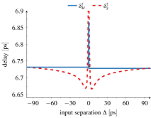
For rising output transitions, the behavior of the NOR is quite different. Each falling input transition causes one of the nMOS to stop conducting while simultaneously one of the pMOS gets closed. Since there is only a single path connecting the output to , the shape of the output signal is essentially independent of ; only the position in time varies. Since the gate only switches after both inputs have changed, the gate delay is . The resulting MIS effect is a (moderate) slow-down, i.e., the gate delay increases for , see Fig. 1b.
III Our Hybrid Model
In this section, we will introduce a model (see Fig. 2b) that replaces transistors by time-varying resistors: The values , thereby vary between some fixed on-resistance and the off-resistance . This results in a hybrid model with 4 different modes, corresponding to the 4 possible input states .
Crucial for our model is choosing a suitable time evolution of in the on- and off-mode, which should facilitate an analytic solution of the resulting ODE systems (4) while being reasonably close to the physical behavior of a transistor. We rely on the very simple Shichman-Hodges transistor model [26], which states a quadratic dependence of the output current on the input voltage. Approximating the latter by in the operation range close to the threshold voltage , with and some fitting parameters, leads to the continuous resistance model
| (1) | ||||
| (2) |
for some constant slope parameters [], [], and on-resistance []; resp. represent the time when the respective transistor is switched on resp. off.
III-A Model development
The arguably most natural idea for developing such a model for the NOR gate would be to maintain explicitly in the state of every ODE system, and switch between those continuously upon a mode switch. However, to begin with, such a “full-state model” would comprise ODE systems with a 5-dimensional state (output voltage and the 4 resistors) and thus render finding an analytic solution hopeless.
We therefore use a different approach, namely, incorporating these resistors only in the coefficients of a simple first-order ODE, which hence become non-constant. Moreover, we employ continuously changing resistors (according to 1) only for switching-on the pMOS transistors. Everything else will be identical to the ideal switch model (which is obtained by setting and ) already employed in [23]. We will argue in Section III-B what guided us to arrive at this model.


Applying Kirchhoff’s rules to Fig. 2b leads to This can be transformed to the non-homogeneous ordinary differential equation (ODE) with non-constant coefficients
| (3) |
using and . Note that the entire voltage divider in Fig. 2b is equivalent to an ideal voltage source and a serial resistor sourcing . Consequently, in 3 is the short-circuit current, and the current actually sourced into . It is well-known that the general solution of (3) is
| (4) |
where denotes the initial condition and .
For simplicity, we will subsequently use the notation , with the abbreviation for the two pMOS transistors and , and , for the two nMOS transistors and .
| Mode | Transition | |||||||||
|---|---|---|---|---|---|---|---|---|---|---|
Table II shows all possible state transitions and the corresponding resistor time evolution mode switches. Double arrows in the mode switch names indicate MIS-relevant modes, whereas and indicate whether switched before or the other way around. For instance, assume the system is in state for quite some time in the past, i.e., and switched to 0 at time . This causes and to be in the on-mode, whereas and are in the off-mode. Now assume that, at time , is switched to 1. This switches resp. to the off-mode resp. on-mode at time . The corresponding mode switch is and reaches state . Now assume that is also switched to 1, at some time . This causes resp. to switch to off-mode resp. on-mode at time . The corresponding mode switch is and reaches state ; note carefully that the delay is -dependent and hence MIS-relevant.
In Section IV, we will determine analytic formulas for the output voltage trajectories given by 4 for every mode switch listed in Table II. Note that, due to the particular modes of the resistors in each transition, different expressions for and according to Table I will be obtained for every mode switch.
III-B Relation to other models
We mentioned already that a 5-dimensional “full-state model” would not allow computing analytic formulas for the trajectories. This is not only disadvantageous for accuracy validation experiments like the ones presented in Section VI, as they must resort to a numerical ODE server, but it also provides no guidance whatsoever for the complex process of model parametrization. Indeed, in Section V, the availability of analytic expressions of the (inverse) trajectories proved instrumental in developing a successful model parametrization process.
Since we conjectured initially that a full-state model should surpass our model proposed in Section III-A in terms of modeling accuracy, however, we nevertheless tried hard to find a suitable parametrization of the FM for the CMOS NOR gate delays given in Fig. 1a and Fig. 1b. Whereas we succeeded to faithfully model the former, we failed to find a parametrization that also covers the latter. Given the large parameter space, we initially blamed our unguided search for the parameters for this failure.
However, as a consequence of another unsuccessful modeling attempt, we eventually diagnosed a deeper reason for this failure. In more detail, as a precursor of our model, we considered a version of the model in Section III-A where both the switching-on and switching-off resistance of all transistors was continuous, according to 1 and 2. However, besides considerably complicating the analysis, it eventually turned out that this model suffers from the same problem as the full-state model: We could not find a parametrization that faithfully covers both Fig. 1a and Fig. 1b.
Thanks to the analytic formulas developed for this precursor model, however, we eventually realized that the parametrization failures are actually a consequence of using the simple resistor model 1 and 2 in operation regions of a transistor where they do not apply. More specifically, consider a rising output transition, i.e., switching-on the serial pMOS transistors and simultaneously switching-off the parallel nMOS transistors in Fig. 2b. Since 1 is a convex function, i.e., eventually decreases sub-linearly, whereas 2 increases linearly, too much of the current provided by the (slowly opening) pMOS transistors is consumed by the (still conducting) nMOS transistors. Consequently, cannot be charged as fast as it should be, no matter how large is chosen. Only the immediate switch of the nMOS transistors, i.e., choosing , allows to circumvent this problem in our setting.222We conjecture that the problem would also disappear if we replaced 1 by a steeper decaying function. However, we do not currently know of a suitable candidate that would render solving our non-constant coefficient ODE 4 possible.
We note that the issue explained above also arises in the case of falling output transitions, albeit less pronounced: The current supplied by the (still conducting but serial) switched-off pMOS transistors can be reasonably swallowed by the the (slowly opening but parallel) nMOS transistors. Nevertheless, we witnessed a trace of this problem, by achieving a lower parametrization and modeling accuracy of the precursor model also for this case.
One other distinguishing feature of our model is its simplicity, besides the need to solve a non-constant coefficient ODE. In particular, whereas the ideal switch model of [23] also incorporates the voltage at the node between the two pMOS transistors (due to the parasitic capacitance ), our model has only one state variable, namely, (due to the load capacitance ). We initially suspected that ignoring in our model could impair its ability to capture some MIS effects, in particular, in the cases of falling input transitions and (recall Section II) where the charge stored in does affect the gate delay. Our results in Section V reveal, however, that this is not the case.
In addition, we tried to keep the number of transistors that actually employ a continuously varying resistance in our model as small as possible: Only the two pMOS transistors and in Fig. 2b use 1, all other resistance switches happen instantaneously.
We conclude this section by stressing again that the general approach of replacing (some) transistors with varying resistors advocated in this paper can be readily applied, and sometimes just transfered, to other gates as well. This is particularly true for the CMOS NAND gate, which is obtained from the NOR gate in Fig. 2b by replacing nMOS transistors with pMOS and vice versa, and swapping and GND. Of course, now the nMOS transistors are the serial ones (where the continuous resistance models must be used). All that is needed to make the results of our analysis matching is to invert the inputs, e.g., by replacing state by and to consider as the output trajectory. Moreover, as our model for the Muller C gate in Section VII confirms, our modeling approach can also be applied easily to other gates, like AOI (and-or-inverter), that involve serial or parallel transistors.
IV Analytic Solutions
In order to verify that the ODE model introduced in Section III faithfully covers all the MIS effects described in Section II, we first derive analytic expressions for the trajectories of for every mode switch listed in Table II. Then, we determine the MIS delays for an arbitrary input separation time as follows:
-
•
Compute , and use it as the initial value for obtaining ; the sought gate delay is the time until the latter crosses the threshold voltage .
-
•
Compute , and use it as the initial value for obtaining ; the sought gate delay is the time until the latter crosses the threshold voltage .
Fortunately, a closer look at Table II and Table I shows a symmetry between the pairs of modes , , , and . Therefore, it is sufficient to derive analytic expressions for the case only. , i.e., to consider the pairs of modes resp. listed above. The corresponding formulas for can be obtained from those by exchanging and as well as and , respectively.
IV-A Rising input transitions
In order to compute , consider the corresponding integrals , , and , as well as in Table I. Since and , we obtain
Since , we get and . With as our initial value, 4 finally provides
| (5) |
Similarly, for the mode , we obtain
such that and . Consequently, we obtain
| (6) |
where can be computed via 5.
Due to the symmetry mentioned before, we can immediately conclude the following result for negative :
| (7) |
where .
IV-B Falling input transitions
In this case, we first need to compute . Again plugging and in the corresponding expressions in Table I provides
With as our initial condition, 4 yields
| (8) |
Now, turning our attention to confronts us with a more intricate case: Whereas again, evaluating requires us to study the function
| (9) |
as
| (10) | ||||
| (11) |
Computing the above integrals is complicated by the fact that also involves the parameter , which prohibits uniform closed-form solutions of 10 and 11. We hence need accurate approximations for , which will be different for different ranges of and , which will in turn depend on the unknown parameters , and . Fortunately, a closer look at the function reveals that piecewise approximations can be built on the basis of (1) distinguishing different ranges (cases) for w.r.t. the parameters , and , and (2) splitting the integration interval into certain subintervals, which may depend on the particular case. Note that this splitting typically also involves an additional free parameter (for some ), which takes care of values of close to . More specifically, we came up with the following four cases and the corresponding approximations for in the appropriate subintervals:
-
•
Case 1: ()
-
•
Case 2: ()
-
•
Case 3: ()
-
•
Case 4: ()
To explain how to determine these approximations, we elaborate on how this is done for Case 1; similar arguments can be used to justify the remaining Cases 2–4. (i) For the range , which expresses the situation where the integration variable is fairly smaller than , we observe , and therefore, . Assuming that the slope parameters and are approximately the same, this leads us to . Furthermore, since here, we get and hence as asserted. (ii) For the range , where is relatively close to , we can substitute by , which leads to . Besides, since , we get , which justifies the asserted approximation for . (iii) Turning our attention to the range , we obtain and hence . Since , this leads to and hence to the asserted approximation. (iv) Finally, for the remaining range , the term is dominant in the denominator of , hence .
It is worth pointing out that we had to split the range into two parts for Case 2 to improve the approximation accuracy, whereas we could merge some ranges for Case 4. Whereas we did not bother to determine analytic bounds for the error of the above first-order Taylor approximations, given the very small absolut values of and , it is clear that it should be very small. This is also confirmed by the model validation simulations in Section V.
The above approximations allow us to easily compute accurate approximations for 10 and 11, and thus to determine the output trajectory , for every choice of . More specifically, depending on different Case , we get , with
| (12) | ||||
| (13) | ||||
| (14) | ||||
| (15) |
which do not depend on . Furthermore,
for Case , where
| (16) |
| (17) |
| (18) |
| (19) |
Combining the above solutions for 10 and 11 according to 4 provides an accurate expression for the output trajectory :
IV-C Single Input Switching
Whereas the main focus of our model is the proper modeling of MIS effects, it of course also needs to handle the “simple” single input switching case. This is done exactly as in the IDM [9], by continuously switching between the trajectories of the modes and (for input A) resp. and (for input B). Fortunately, we can adapt the above trajectory formulas for the MIS cases to also obtain the ones for the SIS cases. In fact, in the SIS cases, just represents the time difference between the current and the previous transition of the same input. For switching from and , for example, it suffices to replace the initial value in by the initial value , which gives the output voltage at the time the previous switch from to .
V Parameterization and Modeling MIS Effects
Since the ultimate goal of our hybrid model is to develop a basis for dynamic digital timing simulations, our main target is the derivation of explicit analytic formulas for the input-to-output delay functions and for both rising and falling output transitions. Moreover, we have to answer the question how to determine the parameters , , , , , , and for a given technology. Such a parametrization is of course necessary for checking whether and how well our new model is capable of faithfully reproducing the MIS effects described in Section II.
To accomplish the first task, by inverting the explicit formulas obtained for the trajectories and resp. for and obtained in the previous section, we obtain the exact resp. approximate analytic expressions for (for ), (for ) and (for ), (for ) in terms of the model’s parameters given in Theorem 1.
Theorem 1 (MIS Delay functions).
For any , the MIS delay functions for falling and rising output transitions of our model are given by:
and, for Case ,
and can be easily obtained by our symmetry.
Proof.
We sketch how is computed; the expression for is obtained analogously. Recall that falling output transitions imply rising input transitions and vice versa. Given the trajectory in 6, we start out from and need to compute the time when either (i) already the preceding trajectory or else (ii) itself (which is started at time ) hits . Note that this reflects the fact that already the first rising input (at time 0) causes the output to switch to 0. Since all these trajectories only involve a single exponential, they are easy to invert. It turns out that case (i) occurs for values , case (ii) for smaller .
Similarly, for computing , we need to consider the trajectory . Here, we have to start out from the initial value and just need to compute the time until hits . This reflects the fact that it is only the second falling input (at time ) that causes the output to switch to 1. ∎
Whereas the specific initial values and used in Theorem 1 are sufficient for evaluating the MIS behavior of our model, we need generalized expressions for the dynamic digital timing simulation experiments in Section VI. In Theorem 2, we therefore provide the delay functions for arbitrary initial values.
Theorem 2 (MIS and SIS delay functions for arbitray initial values).
For any , the extended delay functions for falling and rising output transitions of our model, when starting from a given initial value , are
where and Case . and can be easily obtained by our symmetry.
The delay functions given in Theorem 1 (that is, in Theorem 2) not only facilitate fast dynamic timing analysis, but are also instrumental for understanding which parameters affect the which delay value. In fact, the formulas could even be used for explicit parametrization of a given circuit when certain delay values are known.
V-A Parameterization for 15 nm
In this subsection, we will fit our model to the characteristic MIS delay values , , according to Fig. 1a and the corresponding values , , in Fig. 1b of the CMOS NOR gate implementation described in [23].
Interestingly, our first attempt to simultaneously fit all six delay values for determining all parameters at once turned out to be naive since impossible. To understand why this is the case, note that the on-resistors of the two nMOS transistors and should roughly be the same. Consequently, we obtain
Unfortunately, however, the desired ratio is , which cannot fit these two values with reasonable choices for and . As in [23], we fixed this problem by adding (that is, subtracting) a suitably chosen pure delay (foreseen in the original IDM [9]), which just defers the switching to the new state upon an input transition. This results in an effective ratio of , which could finally be matched by least squares fitting. Of course, when using our model in digital timing analysis, must be added to the computed delay values.
More specifically, starting out from the desired load capacitance , we first determined and by fitting (or ) and to match (or ) and . Once these parameter values had been obtained, we fixed those and determined the remaining parameters , , and by fitting , and to match , and . Note that the same is used for both rising and falling output transitions. The result of our parametrization for the circuit in Section II is shown in Table III.
| Parameters found by fitting the falling output transition case | |||
|---|---|---|---|
| Parameters found by fitting the rising output transition case | |||
Utilizing the parameters in Table III, we can finally visualize the delay predictions of our model. Fig. 3 shows the very good fit for both rising and falling output transitions. We therefore conclude that our new hybrid model fully captures all the MIS effects introduced in Section II, including the case of for rising output transitions where the model proposed in [23] fails.
As a final remark, we note that some of the modeling inaccuracies visible in Fig. 3b are caused by the approximation errors introduced by our solutions of 10 and 11. One is the lack of perfectly fitting the actual delay with the computed one for , which looks quite bad in the figure but actually causes a relative error of about 0.95 % only. Other instances are the small dent shapes around ps, which are caused by the approximation error at the ending boundary of the range in Case 3. It could easily be circumvented by slightly moving the border between Case 3 and Case 4 to a smaller value, i.e., to for some . Since the induced error is marginal, however, we did not bother with further complicating our analysis.
V-B Other parameterizations
A crucial feature of any model is wide applicability. Ideally, our hybrid delay model should be applicable to any CMOS technology, for any supply voltage, temperature, age etc., in the sense that it is possible to determine a parametrization that allows our model to match the MIS delays of any given CMOS NOR implementation. Overall, it is reasonable to conjecture that our model is applicable whenever the Shichman-Hodges transistor model [26], i.e., 1 and 2, reasonably applies. Whereas it is of course impossible for us to prove such a claim, we can demonstrate that this is the case for some quite different technology and operation conditions, namely the UMC technology with supply voltage and a larger load capacitance .333We note that we played with several different conditions and configurations, which all confirmed that the parameters of our model can be easily matched. The red dashed curves in Fig. 4a (falling output) resp. Fig. 4b (rising output), which correspond to Fig. 3a resp. Fig. 3b, show the gate delays depending on the input separation time obtained via SPICE simulations.
Parametrizing our model for these MIS delays turned out to be remarkable easy: Exactly as for our technology, by initially fixing some value for the load capacitance and trying to match (or ) and with (or ) and , we determined accurate values for and . After fixing the latter, we obtained the values of the remaining parameters by fitting the remaining delay values. Note carefully, however, that we had to use a different pure delay here, since . Table IV provides the resulting list of parameters. Not surprisingly, since the gate delay is considerably higher than for our data, we indeed face a significantly larger value for the load capacitance also in our model.
| Parameters found by fitting the falling output transition case | |||
|---|---|---|---|
| Parameters found by fitting the rising output transition case | |||
Utilizing the parameters in Table IV, we finally obtained the blue curves in Fig. 4a and Fig. 4b, which illustrate the computed delays of our model for the technology. It is apparent that they match the real delays very well: We see an ideal fitting for the case of falling output transition as well as for the case of rising output transitions at marginal values. Moreover, considerably promising is the negligible absolute error value of for the mismatch associated with .
VI Modeling Accuracy Experiments
In this section, we experimentally compare the modeling accuracy of our new model to the ideal switch hybrid model [23], the IDM and to classic inertial delays, using the publicly available Involution Tool [14]. Albeit it performs dynamic digital timing simulation in VHDL, it also supports delay models implemented in Python. We hence implemented our model, that is, the delay functions given in Theorem 2, in Python.
For our experimental evaluation, we used the same setup as in [23], namely the Nangate Open Cell Library featuring FreePDK15 FinFET models [27] () that has also been used in Section II. Based on a Verilog description of our NOR gate, we performed optimization, placement and routing by utilizing the Cadence tools Genus and Innovus (version 19.11). We also extracted the parasitic networks from the final layout to obtain SPICE models. These models allowed us to perform simulations with Spectre (version 19.1), which are used to produce golden reference digital signal traces, by recording their crossing times. All simulations in our delay model used the final parameters from Table III. For the ideal switch model and the IDM Exp-channel, the parameters reported in [23] were used.
In order to quantify and compare the typical (average) modeling accuracy of our competing delay models, we stimulated our NOR circuit with randomly generated waveforms. Our experiments targeted both fast (100/50) and slow (200/100) pulse trains on every input, with (LOCAL) and without (GLOBAL) concurrent transitions. For example, the configuration 100/50 - LOCAL of the Involution Tool generates transitions independently on both input A and B, according to a normal distribution with and . The configuration 200/100 - GLOBAL generates transitions either on input A or on B, with and . Each simulation run consisted of 500 transitions and has been repeated 200 times.
As our modeling accuracy comparison metric, we used the area under the deviation trace, which is the absolute value of the difference between the SPICE trace and the trace generated by the respective delay model integrated over time. However, since the absolute values largely depend on the number of transitions, and are therefore meaningless per se, we normalized them with respect to the inertial delays, which is our baseline model. Consequently, lower bars indicate less area under the deviation trace and hence better results. Fig. 5 shows the results of our experiments. It is apparent that our model outperforms the ideal switch hybrid model [23] in the case of fast pulse trains, where the increased modelling accuracy of the falling output MIS delay comes into effect: Around is gained in the case of 100/50 - LOCAL. Whereas this improvement appears to be small, it needs to be stressed that it is the average accuracy that we are evaluating here: Since the randomly generated inputs are unlikely to create many transitions very close to each other (i.e., small ), where the superiority of our model w.r.t. MIS effects for rising output transitions would kick in, one cannot expect much improvement here. In applications like [3], however, pulse trains containing such transitions do occur.
We conclude this section with noting that the simulation times (in the few second-range) for all our models turned out to be similar. More specifically, the inertial delay model (which is natively implemented in ModelSim) is only around 33% faster than both the IDM model and the two hybrid models in all our configurations. Given that both hybrid models have been implemented in Python, we can safely say that predicting gate delays using our new model does not incur a significant overhead in terms of simulation running times. Whereas it appears that the simulation times in SPICE also match the ones of ModelSim in configurations like 100/50 - LOCAL and the ones of our hybrid models in 5000/5 - GLOBAL, this is only due to the fact that the simulated circuit is so small. As already mentioned in Section I, the SPICE simulation times quickly go up with the number of transistors in the circuit.
VII Hybrid Delay Models for Other Gates
In this section, we will demonstrate that our general approach can be applied to other gates as well. We mentioned already at the end of Section III-A that our results for the NOR gate can be transferred to the case of a NAND gate by simply swapping nMOS transistors with pMOS transistors and vice versa, as well as swapping the supply voltage ( and GND). In addition, we mentioned that, in some recent work that could not be referenced for anonymity reasons, we extended our model for the NOR gate by adding an RC interconnect and experimentally verified its very good accuracy.
More generally, we believe that it is easy to apply our modeling approach to any CMOS gate that involves serial and parallel transistors only, like Muller C gates Cand AOI (and-or-inverter) gates. We will demonstrate this for the Muller C gate, which plays a prominent role in many asynchronous circuit designs, like the one [3] already mentioned in Section I.
We will apply our approach to the CMOS implementation of C shown in Fig. 6a, which involves a state keeper element made up of a loop of two inverters. Whereas this seems to complicate our modeling at first sight, it turns out that we can safely drop it from our considerations altogether: The (ideal) load capacitance in the corresponding resistor model Fig. 6b acts as the state keeper for in the case the output is in a high-impedance state, i.e., when both at least one of and and at least one of and are switched off. In order to accommodate the negation of the output, we just let and correspond to the nMOS transistors and , and and to the pMOS transistors and .
Similar to the NOR gate, we use continuously varying resistors according to 1 for the switching-on and instantaneous switching-off, but this time for all transistors. Applying Kirchhoff’s rules to Fig. 6b leads to the first-order non-homogeneous ordinary differential equation (ODE) with non-constant coefficients
| (21) |
where and . It is not difficult to check that a similar solution approach as described in Section IV leads to the following expressions for the output voltage, for rising resp. falling input transitions and , corresponding to 5 and 6 resp. 8 and 20:
with and as the initial values of the transitions , and , respectively. Herein, and are defined exactly as in 12 to Section IV-B with substituting by . Similarly, and are obtained by replacing , with , in 12 to Section IV-B. Finally, the following theorem, whose proof is very similar to the one for Theorem 2, provides the delay formulas for the C gate.
Theorem 3 (MIS and SIS delay functions for the C gate, for arbitray initial values).
For any , the delay functions for falling and rising output transitions of our model, when starting from a given initial value , are
As for the NOR gate, the trajectory and delay formulas for can be easily obtained by the symmetry mentioned in Section IV.

We demonstrate the good accuracy of this hybrid delay model by comparing the model predictions and the SPICE simulation data for a nm CMOS technology C gate. For model parametrization, we could re-use the procedure for the NOR gate, which provided the parameters listed in in Table V. The comparison results are shown in Fig. 6c and Fig. 6d.
VIII Conclusions
We provided a novel approach for developing hybrid delay models for dynamic timing analysis of CMOS gates, and showed that it is capable of faithfully covering all MIS effects in the case of a NOR gate and a Muller C gate. Relying on a first-order model of dimension 1, the resulting model for the NOR gate is even simpler than the immediate switch hybrid ODE model proposed in [23], albeit it does not share its failure to model the MIS effect for rising output transitions. Thanks to its simplicity, it allows to compute accurate approximation formulas for the gate delays, which makes the model efficiently applicable in dynamic digital timing analysis and facilitates easy model parametrization. An experimental comparison of the modeling accuracy against alternative approaches confirmed its superior performance.
References
- [1] CCS Timing Library Characterization Guidelines, Synopsis Inc., October 2016, version 3.4.
- [2] Effective Current Source Model (ECSM) Timing and Power Specification, Cadence Design Systems, January 2015, version 2.1.2.
- [3] A. J. Winstanley, A. Garivier, and M. R. Greenstreet, “An Event Spacing Experiment,” in Proceedings of the 8th International Symposium on Asynchronous Circuits and Systems (ASYNC), April 2002, pp. 47–56.
- [4] S. Furber, “Large-scale neuromorphic computing systems,” Journal of Neural Engineering, vol. 13, no. 5, p. 051001, aug 2016. [Online]. Available: https://doi.org/10.1088/1741-2560/13/5/051001
- [5] M. Bouvier, A. Valentian, T. Mesquida, F. Rummens, M. Reyboz, E. Vianello, and E. Beigne, “Spiking neural networks hardware implementations and challenges: A survey,” J. Emerg. Technol. Comput. Syst., vol. 15, no. 2, apr 2019. [Online]. Available: https://doi.org/10.1145/3304103
- [6] L. Nagel and D. O. Pederson, “Spice (simulation program with integrated circuit emphasis),” 1973.
- [7] F. N. Najm, “A survey of power estimation techniques in vlsi circuits,” IEEE Transactions on Very Large Scale Integration (VLSI) Systems, vol. 2, no. 4, pp. 446–455, 1994.
- [8] M. J. Bellido-Díaz, J. Juan-Chico, and M. Valencia, Logic-Timing Simulation and the Degradation Delay Model. London: Imperial College Press, 2006.
- [9] M. Függer, R. Najvirt, T. Nowak, and U. Schmid, “A faithful binary circuit model,” IEEE Transactions on Computer-Aided Design of Integrated Circuits and Systems, vol. 39, no. 10, pp. 2784–2797, 2020.
- [10] S. H. Unger, “Asynchronous sequential switching circuits with unrestricted input changes,” IEEE Transaction on Computers, vol. 20, no. 12, pp. 1437–1444, 1971.
- [11] M. Függer, T. Nowak, and U. Schmid, “Unfaithful glitch propagation in existing binary circuit models,” IEEE Transactions on Computers, vol. 65, no. 3, pp. 964–978, March 2016.
- [12] M. Függer, J. Maier, R. Najvirt, T. Nowak, and U. Schmid, “A faithful binary circuit model with adversarial noise,” in 2018 Design, Automation Test in Europe Conference Exhibition (DATE), March 2018, pp. 1327–1332. [Online]. Available: https://ieeexplore.ieee.org/document/8342219/
- [13] D. Öhlinger and U. Schmid, “A digital delay model supporting large adversarial delay variations,” 2023, (to appear at DDECS’23).
- [14] D. Öhlinger, J. Maier, M. Függer, and U. Schmid, “The involution tool for accurate digital timing and power analysis,” Integration, vol. 76, pp. 87 – 98, 2021.
- [15] R. Najvirt, U. Schmid, M. Hofbauer, M. Függer, T. Nowak, and K. Schweiger, “Experimental validation of a faithful binary circuit model,” in Proceedings of the 25th Edition on Great Lakes Symposium on VLSI, ser. GLSVLSI ’15. New York, NY, USA: ACM, 2015, pp. 355–360. [Online]. Available: http://doi.acm.org/10.1145/2742060.2742081
- [16] L.-C. Chen, S. K. Gupta, and M. A. Breuer, “A new gate delay model for simultaneous switching and its applications,” in Proceedings of the 38th Design Automation Conference (IEEE Cat. No.01CH37232), 2001, pp. 289–294.
- [17] A. R. Subramaniam, J. Roveda, and Y. Cao, “A finite-point method for efficient gate characterization under multiple input switching,” ACM Trans. Des. Autom. Electron. Syst., vol. 21, no. 1, pp. 10:1–10:25, Dec. 2015. [Online]. Available: http://doi.acm.org/10.1145/2778970
- [18] J. Shin, J. Kim, N. Jang, E. Park, and Y. Choi, “A gate delay model considering temporal proximity of multiple input switching,” in 2009 International SoC Design Conference (ISOCC), Nov 2009, pp. 577–580.
- [19] V. Chandramouli and K. A. Sakallah, “Modeling the effects of temporal proximity of input transitions on gate propagation delay and transition time,” in Proc. DAC’96, 1996, p. 617–622. [Online]. Available: https://doi.org/10.1145/240518.240635
- [20] J. Sridharan and T. Chen, “Modeling multiple input switching of cmos gates in dsm technology using hdmr,” in Proceedings of the Design Automation Test in Europe Conference, vol. 1, March 2006, pp. 6 pp.–.
- [21] O. V. S. Shashank Ram and S. Saurabh, “Modeling multiple-input switching in timing analysis using machine learning,” IEEE Transactions on Computer-Aided Design of Integrated Circuits and Systems, vol. 40, no. 4, pp. 723–734, 2021.
- [22] J. C. Ebergen, S. Fairbanks, and I. E. Sutherland, “Predicting performance of micropipelines using charlie diagrams,” in Proceedings Fourth International Symposium on Advanced Research in Asynchronous Circuits and Systems (ASYNC’98), 1998, pp. 238–246.
- [23] A. Ferdowsi, J. Maier, D. Öhlinger, and U. Schmid, “A simple hybrid model for accurate delay modeling of a multi-inpu t gate,” in Proceedings of the 2022 Design, Automation & Test in Europe Confer ence & Exhibition, ser. DATE ’22, 2022.
- [24] T. A. Henzinger, The Theory of Hybrid Automata. Berlin, Heidelberg: Springer Berlin Heidelberg, 2000, pp. 265–292.
- [25] A. Ferdowsi, M. Függer, T. Nowak, and U. Schmid, “Continuity of thresholded mode-switched odes and digital circuit delay models,” 2023, (to appear in HSCC’23).
- [26] H. Shichman and D. A. Hodges, “Modeling and simulation of insulated-gate field-effect transistor switching circuits,” IEEE Journal of Solid-State Circuits, vol. 3, no. 3, pp. 285–289, Sep. 1968.
- [27] M. Martins, J. M. Matos, R. P. Ribas, A. Reis, G. Schlinker, L. Rech, and J. Michelsen, “Open cell library in 15nm freepdk technology,” in Proceedings of the 2015 Symposium on International Symposium on Physical Design, ser. ISPD ’15. New York, NY, USA: ACM, 2015, pp. 171–178. [Online]. Available: http://doi.acm.org/10.1145/2717764.2717783