Silicon anisotropy in a bi-dimensional optomechanical cavity
Abstract
In this work, we study the effects of mechanical anisotropy in a 2D optomechanical crystal geometry. We fabricate and measure devices with different orientations, showing the dependence of the mechanical spectrum and the optomechanical coupling with the relative angle of the device to the crystallography directions of silicon. Our results show that the device orientation strongly affects its mechanical band structure, which makes the devices more susceptible to fabrication imperfections. Finally, we show that our device is compatible with cryogenic measurements reaching ground state occupancy of 0.2 phonons at mK temperature.
In the last decade, optomechanical crystal cavities have been shown to confine light and mechanical motion in sub-wavelength modal volumes, leading to high optomechanical coupling rates Leijssen et al. (2017); Balram et al. (2014); Chan et al. (2012) () and long-lived mechanical excitations Alegre et al. (2011); MacCabe et al. (2020). Through the careful choice of geometry and material the photon-phonon interaction can be tailored, enabling applications not only in the classical realm, such as microwave phonon routing Fang et al. (2016) and high frequency phonon sources Navarro-Urrios et al. (2015), but also in the quantum domain, such as sideband ground-state cooling Chan et al. (2011), optomechanical quantum memories Wallucks et al. (2020a) and remote quantum state transfer in mechanical dual-rail encoded qubits Fiaschi et al. (2021).
Most of the optomechanical crystal devices used in quantum experiments are based on suspended quasi-one-dimensional (1D) beam structures. These devices combine large optical and mechanical quality factors with high in a simple design. However, such quasi-1D geometries present a fundamental drawback since they usually do not have good thermal dissipation and even the faintest light pulses can heat a device away from its mechanical ground state MacCabe et al. (2020); Wallucks et al. (2020b). In contrast, quasi-two-dimensional (2D) structures Benevides et al. (2017); Alegre et al. (2011); Ren et al. (2020) have already been demonstrated to have impressive optical quality factors Sekoguchi et al. (2014) and could have a much better thermal conductance. Nonetheless, few experimental works have focused on hypersonic (>GHz) quasi-2D optomechanical crystal Ren et al. (2022); Florez et al. (2022) devices due to their more complex design and fabrication process. In this case, material crystalline anisotropy, known to affect the performance of quasi 1D-optomechanical devices Jiang et al. (2019); Burgwal and Verhagen (2022); Balram et al. (2014), becomes even more important. In this work, we study through simulation, fabrication, and measurements, the impacts of the mechanical anisotropy on a silicon-based cavity using the recently proposed design from Ref. Ren et al., 2020. We then achieve high optomechanical coupling and low-phonon number occupancy necessary for quantum experiments.
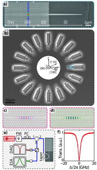
The device’s geometry consists of a quasi-1D cavity composed of two lines of C-shaped holes facing each other surrounded by a 2D triangular lattice of snowflake-shaped holes (Fig. 1 a). The snowflake structure allows for large optical and mechanical band gaps Safavi-Naeini and Painter (2010); Safavi-Naeini et al. (2014) that confine the modes within the C-shape region while still providing a good path for thermal dissipation compared to quasi-1D designs. The final devices, shown in Figs. 1 a-b, are based on a traditional top-bottom fabrication process using a silicon-on-insulator (SOI) wafer. They are composed of: (i) a -long suspended tapered waveguide that efficiently couples Gröblacher et al. (2013) light from either a lensed fiber or a silica tapered fiber to a wide waveguide; (ii) a coupler region composed of eight transition cells, where the regular waveguide geometry is slowly morphed into the C-shape mirror unit cell, avoiding strong reflections due to impedance mismatching (see supplementary material for the specific geometry); (iii) a symmetrical defect region composed of 14 cells, whose dimensions are varied from the mirror unit cell at its edges to the defect unit cell at its center, confining both optical (Fig. 1 c) and mechanical (Fig. 1 d) modes; and finally (iv) a mirror region composed of eight mirror cells, placed at the end of the structure to avoid optical and mechanical leakage. The devices are fabricated at a given angle () defined as the counter-clockwise angle between the crystalline direction and the axis geometry while keeping the axis perpendicular to the wafer plane, which in our case is aligned to the direction. For a more detailed description of the fabricated design and of the fabrication process we refer the reader to section S1 of the Supplemental Material.
Fig. 1 e shows the basic experimental setup used to measure both the optical and mechanical properties of the devices. It consists of a tunable laser, connected to an optical fiber circuit leading to a tapered fiber that couples light to the integrated tapered waveguides in our devices. Using a circulator before the tapered fiber we recover the reflection signal from our devices. With the aid of a data acquisition card and a slow photodetector, we measure the optical response of the cavities while slowly scanning the laser frequency, allowing us to characterize their optical response as a function of the detuning between the laser and the optical mode frequency, as shown in Fig. 1 f. A fast detector attached to an electrical signal analyzer (ESA) is used to measure the Power Spectral Density (PSD) of the optical signal, showing the transduction of the mechanical spectrum due to the Brownian motion. The optomechanical coupling is then measured by comparing the intensity of the mechanical peaks with the intensity of a calibrated side-band introduced by a phase modulator, as proposed in Gorodetksy et al., 2010.
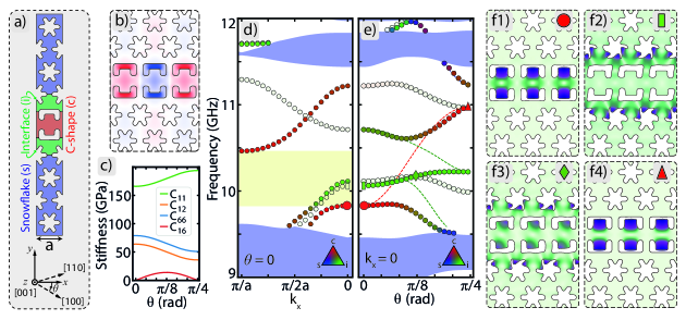
In order to understand the fundamental impact of the mechanical anisotropy in the optomechanical coupling rate and mechanical mode confinement, we use Finite Element Method (FEM) simulations. Initially we explore how affects the band structure of a mechanical waveguide based on the 1D mirror unit cell of our devices (Fig. 2 a). These propagating modes are classified according to the symmetries of the waveguide, which are a composition of the symmetries arising from the unit-cell geometry and the silicon material properties. Understanding in detail such symmetries will allow us to better appreciate the behavior of the whole device, encompassing the mirror and the defect region.
The unit cell geometry in Fig. 2 a presents symmetry with respect to inversion about the and axis ( and ), nevertheless, Floquet periodicity over the axis is such that symmetry is only valid for modes at the center or at the edges of the Brillouin zone ( or ). The components of the silicon stiffness tensor can also be classified according to the and symmetries. The basic components , and present even symmetry, while the component , which couples compressive and shear stresses, is the only one that presents odd symmetry (Fig. 2 c).
Due to the component, in general, the symmetry that is shared between the unit cell geometry and the material properties is a rotation of over the axis (). Nevertheless, for and the axis is aligned with the and crystallographic directions of silicon respectively, restoring the and symmetries as the component is null at these angles (Fig. 2 c).
In Fig. 2 d we present the mechanical band diagram for where the colored dots represent modes with even symmetry regarding (). The RGB color of the dots indicates the ratio of the displacement energy in each one of the highlighted regions in Fig. 2 a: the C-shape (red), the interface (green) and the snowflake (blue) regions. Transparent dots are modes with odd symmetry (), which do not couple with the even mechanical modes. When we consider only bands strongly confined at the C-shape region (red dots) we identify the apparent band gap highlighted by the yellow-shaded region in Fig. 2 d. This is not a true band gap, since a spurious interface band crosses it away from region.
The defect of our optomechanical crystal cavity was designed (see Supplemental Material S1) to confine the mode from the bottom C-shape band at , which is shown in Fig. 2 f1. Despite the absence of a true phononic band gap, one can still achieve strong confinement as long as there is no significant energy exchange between the confined mode in question and the spurious interface modes Eichenfield et al. (2009). One of the factors limiting the coupling between those modes in the optomechanical cavity is the fact that at and the C-shape mode (Fig. 2 f1) is the only one that presents even symmetry for both and . Additionally, the energy transfer from the C-shape to the spurious interface modes is inhibited by the much lower quality factor of the latter.
In Fig. 2 e we present the mechanical modes at the center of the Brillouin zone (), and the dashed lines show the band structure with set to zero. In this artificial case, the C-shape mechanical mode (red dashed line) keeps its symmetry and remains a pure C-shape mode. Its frequency monotonically increases with , following the component related to pure compression, while it crosses modes with distinct symmetries located at the interface (green dashed lines). However, in the real case, the shear stress promoted by the component deforms the mechanical modes which are no longer symmetric under and , but are still symmetric under . The colored dots represent modes with even symmetry concerning (), while transparent dots present modes with . The color scheme is the same one used in the Fig. 2 d and represents the energy distribution in the geometry. As we go from to , the C-shape (Fig. 2 f1) and interface modes with the same symmetry, e.g. Fig. 2 f2, couple to each other leading to the large anti-crossing seen in Fig. 2 e. Consequently, there is no pure C-shape mode at but only mixed modes as the one shown in Fig. 2 f3. Furthermore, the anisotropy induced symmetry break and the strong delocalization away from the C-shape region decrease the overlap of such modes with the optical mode (Fig. 2 b), decreasing their optomechanical coupling.
As goes from to the value of the component decreases towards zero, the C-shape and interface modes become decoupled once again. At , the original band gap does not exist anymore and a new band gap is formed between the C-shaped mode and the higher frequency snowflake modes (upper blue shaded region). There is also an interface mode very close in frequency to the C-shape mode and although, at , these two modes have distinct symmetry, both have similar quality factors and share symmetry, and, as such, fabrication imperfections are likely to couple them with each other. In addition, both bands present a flat dispersion near (see supplementary), making them even more susceptible to such imperfections Safavi-Naeini et al. (2014).
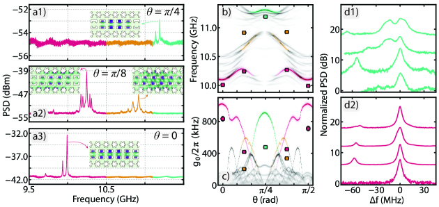
Understanding the band structure upon which our optomechanical crystal cavity is based we then measured the devices shown in Fig. 1 b. The mechanical spectra of devices fabricated at , , and are shown in Figs. 3 a1-a3 respectively. Figs. b and c present the results of the simulation for the whole device, encompassing both the mirror and the defect region. Fig. 3 b shows the frequencies of the simulated mechanical modes as a function of , while Fig. 3 c shows the optomechanical coupling. The modes with the highest values in different frequency ranges are highlighted using the same color code as in Figs. 3 a1-a3, defining mode branches. Both the experimental data and the simulations for the whole device follow the same behavior as in the waveguide simulations, where the frequency of the high C-shape modes increases as varies from to , with a sudden frequency jump around due to the anti-crossing of C-shape and interface modes. As shown in Fig. 3 c), when passing through such anti-crossing the optomechanical coupling is transferred from one branch to the other. Inside the red branch, we also find a similar behavior with falling steeply due to a small anti-crossing with another interface mode in between and .
The displacement profiles shown in the insets of Fig. 3 a1-a3 illustrate this picture. The C-shape mode at is concentrated at the C-shape region, overlapping with the optical mode on the airgap. At hybridization occurs due to the anisotropy, and the mechanical displacement profile extends from the C-shape into the interface region, lowering the optomechanical overlap. Finally, for the displacement profile becomes again concentrated at the C-shape region. It is interesting to notice that the optomechanical coupling is higher for than for . This happens because the mode at is more spread along the C-shape region than the mode at 111This is related to the flat dispersion of the C-shape mode at which leads to a high spectral density and consequently to modes very concentrated at few defect unit-cells., in such a way that the former has a better overlap with the optical mode.
The squares in Fig. 3 b) indicate the frequencies of the mechanical modes with the highest measured Gorodetksy et al. (2010) (see the S3 supplementary material for details on measurement). They agree within 1% with the converged frequencies from the simulation. The optomechanical couplings on the other hand are not as well predicted as the frequencies, with the average highest measured varying between and of the simulated values for and respectively. This indicates that the devices at are more robust to fabrication imperfections than the ones at . The comparison of different devices fabricated at the same orientation, shown in Figs. 3 d1 and d2, corroborates this analysis. For the spectra of multiple devices, are similar to each other, usually presenting a mode with between and , with a secondary mode at a frequency lower, which corresponds quite well with the simulated second order C-shape mode. For the spectra are quite different among different devices and present multiple overlapping modes. Such lack of repeatability for can be attributed to the presence of flat C-shape and interface bands in the waveguide band structure, as discussed in Figs. 2 e.
For the comparison between simulation and experiment is more difficult as the estimated imprecision on the simulation of hybrid modes is larger (+4%) than for the pure C-shape modes. Due to computational limitations, we cannot pinpoint the exact contribution of each interface mode to the measured modes, nevertheless, it is clear that multiple interface modes hybridize with the C-shape mode to form the two clusters of modes shown in Fig. 3 a2.
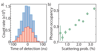
As a demonstration of the compatibility of such devices with quantum optomechanics experiments, we measure below 1 phonon occupancies, placing them in a dilution fridge reaching base temperatures. The phonon occupancy () is measured using sideband asymmetry photon counting Meenehan et al. (2015). When a laser is fed in an optomechanical device, the interaction can be understood in terms of Stokes (anti-Stokes) processes in which one phonon is created (annihilated), while the frequency of one photon is decreased (increased) by one mechanical frequency (). The likelihood of such scattering processes depends on the detuning, , of the laser relative to the optical resonance frequency. Stokes processes are maximum when the laser is blue-detuned by one mechanical frequency (), in contrast, anti-Stokes processes are maximum when the laser is red-detuned ().
To perform such an experiment we have used laser pulses that could be tuned to the blue and red sidebands. To avoid extra heating of the mechanical mode and guarantee that the initial state of the cavity is always the same, the laser pulses were tuned to be wide with period. The scattered photons were filtered, using wide Fabry-Pérot filters, and sent to single photon detectors. The filtering efficiency of the incident laser in both sidebands was on the order of .
Fig. 4 a shows an example of the scattering count rates obtained for the blue and red sidebands. As expected, we obtain different scattering rates for the two sidebands. In Fig 4b, we show the resulting occupancy for different scattering probabilities (experimentally controlled via the pulse power), showing that falls as the probability is decreased. Moreover, with scattering probabilities below approximately (corresponding to approximately ), we obtain an average occupation level lower than phonon in the system achieving a smaller occupation number for lower power, albeit with larger errors due to dark counts and leaking photons in the system.
As the research on optomechanical devices progresses towards more complex materials, such as lithium niobate Jiang et al. (2019) and gallium phosphide Stockill et al. (2022); Schneider et al. (2019), understanding the interplay between device geometry and material anisotropy will become increasingly important. Here we have studied how the silicon mechanical anisotropy affects the properties of our bi-dimensional optomechanical crystals. The mechanical anisotropy was shown to couple C-shape and interface modes, decreasing the overall optomechanical coupling. This effect can be mitigated by choosing orientations in which the device geometry shares the same symmetries as the device geometry, and in our case. However, even at these angles, such couplings can still be relevant. In the future, we intend to investigate how to further suppress such couplings by the proper engineering of the interface region. For example, by stretching in the vertical direction the first line of snowflake holes it is possible to decrease the frequency of the interface modes changing their spectral distance from the c-shape mode at . Finally, we also demonstrate that under passive cooling phonon occupations as low as 0.2 phonons can be measured, demonstrating, in conjunction with the thermal stability shown in Ren et al., 2020, its viability as a platform for quantum optomechanics experiments.
SUPPLEMENTARY MATERIAL
See Supplementary Material S1 for details on C-shape geometry design and fabrication. S2 provides a comprehensive description of the waveguide band structure for different crystalline orientations. Finally, in S3 a detailed discussion of the optomechanical measurement and calibration is presented.
ACKNOWLEDGMENTS
The authors would like to acknowledge assistance from the Kavli Nanolab Delft and CCSNano-UNICAMP with the micro-fabrication infrastructure. This work was supported by São Paulo Research Foundation (FAPESP) through grants 2019/01402-1, 2020/06348-2, 2020/00119-1, 2020/00100-9, 2022/07719-0, 2018/15580-6, 2018/15577-5, 2018/25339-4, Coordenação de Aperfeiçoamento de Pessoal de Nível Superior - Brasil (CAPES) (Finance Code 001), Financiadora de Estudos e Projetos (Finep), the European Research Council (ERC CoG Q-ECHOS, 101001005), and by the Netherlands Organization for Scientific Research (NWO/OCW), as part of the Frontiers of Nanoscience program, as well as through Vrij Programma (680-92-18-04).
DATA AVAILABILITY
FEM and scripts files for generating each figure will be available at Ref. Kersul et al., 2022. Additional data that support the findings of this study are available from the corresponding author upon reasonable request.
References
- Leijssen et al. (2017) R. Leijssen, G. R. La Gala, L. Freisem, J. T. Muhonen, and E. Verhagen, Nature Communications 8, 1 (2017), arXiv:1612.08072 .
- Balram et al. (2014) K. C. Balram, M. Davanço, J. Y. Lim, J. D. Song, and K. Srinivasan, Optica 1, 414 (2014).
- Chan et al. (2012) J. Chan, A. H. Safavi-Naeini, J. T. Hill, S. Meenehan, and O. Painter, Applied Physics Letters 101, 081115 (2012).
- Alegre et al. (2011) T. P. M. Alegre, A. Safavi-Naeini, M. Winger, and O. Painter, Opt. Express 19, 5658 (2011).
- MacCabe et al. (2020) G. S. MacCabe, H. Ren, J. Luo, J. D. Cohen, H. Zhou, A. Sipahigil, M. Mirhosseini, and O. Painter, Science 370, 840 (2020).
- Fang et al. (2016) K. Fang, M. H. Matheny, X. Luan, and O. Painter, Nature Photonics (2016), 10.1038/nphoton.2016.107.
- Navarro-Urrios et al. (2015) D. Navarro-Urrios, N. E. Capuj, J. Gomis-Bresco, F. Alzina, A. Pitanti, A. Griol, A. Martínez, and C. M. S. Torres, Scientific Reports 5, 15733 (2015).
- Chan et al. (2011) J. Chan, T. P. M. Alegre, A. H. Safavi-Naeini, J. T. Hill, A. Krause, S. Gröblacher, M. Aspelmeyer, and O. Painter, Nature 478, 89 (2011).
- Wallucks et al. (2020a) A. Wallucks, I. Marinković, B. Hensen, R. Stockill, and S. Gröblacher, Nature Physics 16, 772 (2020a).
- Fiaschi et al. (2021) N. Fiaschi, B. Hensen, A. Wallucks, R. Benevides, J. Li, T. P. M. Alegre, and S. Gröblacher, Nature Photonics 15, 817 (2021).
- Wallucks et al. (2020b) A. Wallucks, I. Marinković, B. Hensen, R. Stockill, and S. Gröblacher, Nature Physics 16, 772 (2020b), arXiv:1910.07409 .
- Benevides et al. (2017) R. Benevides, F. G. S. Santos, G. O. Luiz, G. S. Wiederhecker, and T. P. M. Alegre, Scientific Reports 7, 2491 (2017), arXiv:1701.03410 .
- Ren et al. (2020) H. Ren, M. H. Matheny, G. S. MacCabe, J. Luo, H. Pfeifer, M. Mirhosseini, and O. Painter, Nature Communications 11, 3373 (2020), arXiv:1910.02873 .
- Sekoguchi et al. (2014) H. Sekoguchi, Y. Takahashi, T. Asano, and S. Noda, Optics Express 22, 916 (2014).
- Ren et al. (2022) H. Ren, T. Shah, H. Pfeifer, C. Brendel, V. Peano, F. Marquardt, and O. Painter, Nature Communications 13, 3476 (2022).
- Florez et al. (2022) O. Florez, G. Arregui, M. Albrechtsen, R. C. Ng, J. Gomis-Bresco, S. Stobbe, C. M. Sotomayor-Torres, and P. D. García, Nature Nanotechnology 17, 947 (2022).
- Jiang et al. (2019) W. Jiang, R. N. Patel, F. M. Mayor, T. P. McKenna, P. Arrangoiz-Arriola, C. J. Sarabalis, J. D. Witmer, R. V. Laer, and A. H. Safavi-Naeini, Optica 6, 845 (2019).
- Burgwal and Verhagen (2022) R. Burgwal and E. Verhagen, arXiv preprint arXiv:2207.11114 (2022).
- Safavi-Naeini and Painter (2010) A. H. Safavi-Naeini and O. Painter, Optics Express 18, 14926 (2010).
- Safavi-Naeini et al. (2014) A. H. Safavi-Naeini, J. T. Hill, S. Meenehan, J. Chan, S. Gröblacher, and O. Painter, Phys. Rev. Lett. 112, 153603 (2014).
- Gröblacher et al. (2013) S. Gröblacher, J. T. Hill, A. H. Safavi-Naeini, J. Chan, and O. Painter, Applied Physics Letters 103, 181104 (2013), https://doi.org/10.1063/1.4826924 .
- Gorodetksy et al. (2010) M. L. Gorodetksy, A. Schliesser, G. Anetsberger, S. Deleglise, and T. J. Kippenberg, Opt. Express 18, 23236 (2010).
- Eichenfield et al. (2009) M. Eichenfield, J. Chan, A. H. Safavi-Naeini, K. J. Vahala, and O. Painter, Opt. Express 17, 20078 (2009).
- Note (1) This is related to the flat dispersion of the C-shape mode at which leads to a high spectral density and consequently to modes very concentrated at few defect unit-cells.
- Meenehan et al. (2015) S. M. Meenehan, J. D. Cohen, G. S. MacCabe, F. Marsili, M. D. Shaw, and O. Painter, Phys. Rev. X 5, 041002 (2015).
- Stockill et al. (2022) R. Stockill, M. Forsch, F. Hijazi, G. Beaudoin, K. Pantzas, I. Sagnes, R. Braive, and S. Gröblacher, Nature Communications 13, 1 (2022).
- Schneider et al. (2019) K. Schneider, Y. Baumgartner, S. Hönl, P. Welter, H. Hahn, D. J. Wilson, L. Czornomaz, and P. Seidler, Optica 6, 577 (2019).
- Kersul et al. (2022) C. M. Kersul, R. Benevides, F. Moraes, G. H. M. de Aguiar, A. Wallucks, S. Gröblacher, G. S. Wiederhecker, and T. P. M. Alegre, “Data and simulation files for: "Silicon anisotropy in a bi-dimensional optomechanical cavity",” (2022).