Anomalous conductance scaling in Weyl semimetal NbAs
Abstract
Protected surface states arising from non-trivial bandstructure topology in semimetals can potentially enable new device functionalities in compute, memory, interconnect, sensing, and communication. This necessitates a fundamental understanding of surface-state transport in nanoscale topological semimetals. Here, we investigate quantum transport in a prototypical topological semimetal NbAs to evaluate the potential of this class of materials for beyond-Cu interconnects in highly-scaled integrated circuits. Using density functional theory (DFT) coupled with non-equilibrium Green’s function (NEGF) calculations, we show that the resistance-area product in NbAs films decreases with decreasing thickness at the nanometer scale, in contrast to a nearly constant product in ideal Cu films. This anomalous scaling originates from the disproportionately large number of surface conduction states which dominate the ballistic conductance by up to 70 in NbAs thin films. We also show that this favorable scaling persists even in the presence of surface defects, in contrast to sharply increasing with reducing thickness for films of conventional metals, such as Cu, in the presence of surface defects. These results underscore the promise of topological semimetals like NbAs as future back-end-of-line (BEOL) interconnect metals.
IBM Thomas J. Watson Research Center, 1101 Kitchawan Road, Yorktown Heights, NY 10598
TOC Image:
![[Uncaptioned image]](/html/2211.10426/assets/x1.png)
Keywords: Weyl semimetal, topological protection, electrical resistivity, surface scattering
1 Introduction
The discovery of Weyl semimetals and topological semimetals in general 1, 2, 3, 4, 5, 6, 7, 8, 9 has prompted research into new phenomena and exciting applications in various areas of condensed matter physics. These include usage as far-infrared and tetrahertz detectors 10, magnetoresistive memory devices 11, 12, photovoltaic devices 13, and as interconnects in next-generation integrated circuits (ICs) 14, 15, 16, 17. A Weyl semimetal can be formed by breaking either time-reversal or inversion symmetry in a crystal with 3D Dirac cones, leading to pairs of band crossing points called Weyl nodes. The surface Brillouin Zone of Weyl semimetals have projections of such Weyl node pairs connected through series of topologically-protected Fermi-arc surface states 3. Substantial recent research efforts have targeted first-principles prediction of new topological semimetals, material syntheses, and confirmation of nontrivial band structures and Fermi-arc surface states using angle-resolved photoemission spectroscopy (ARPES) 9, 5, 6, 7, 8. These materials have been shown to exhibit novel transport, optical and magnetic phenomena 18, 19, 20, 21, including chiral anomalies 22, a nonlinear Hall effect 23, 24, 25, a quantized circular photogalvanic effect 26, 27, 28 and giant second-harmonic generation 10, 29.
Like topological insulators, the surface states of topological semimetals have received considerable attention, which if topologically protected, could potentially lead to high surface conduction. Previous theoretical work has argued that the Fermi-arc states in a toy-model Weyl semimetal contribute the same order of magnitude as the bulk states to total conduction 30 and could be highly disorder tolerant when the Fermi arcs are nearly straight 31. However, other studies have shown that the transport due to Fermi arcs is dissipative due to a strong hybridization of surface and bulk states, which leads to scattering between surface and bulk states 32, 33. Since these studies relied primarily on highly-simplified Hamiltonians and analytical models, a comprehensive study of transport fully accounting for the electronic structure at dimensions relevant to future device applications is now necessary.
In this work, we pursue a fundamental understanding of electron transport properties of Weyl semimetals at nanoscale and evaluate their potential as high conductivity future interconnect metals. In modern-day ICs, the devices patterned on a silicon substrate are linked to form a circuit using Cu nanowires called interconnects. The resistivity of Cu increases dramatically with decreasing size due to enhanced scattering of electrons from surfaces, defects, and grain boundaries 34, 35, 36, 37. Such increase in the resistivity can increase the signal delay and energy consumption by , a major bottleneck in the semiconductor industry 16, 38. The search to replace Cu has expanded from elemental metals to intermetallics 39, 40, 41, 42, metallic carbides and nitrides such as MAX phases 43, 44, directional conductors 45, and topological materials 14, 15, 46, 47, 17.
In a recent breakthrough, Zhang et al. 48 showed experimentally that the electrical resistivity of nanobelts of [001] oriented NbAs, a Weyl semimetal, becomes an order of magnitude lower than the bulk single-crystal resistivity. In some nanobelt samples, the resistivity can even be lower than the bulk resistivity of Cu. Such an anomalous reduction was attributed to transport via the disorder-tolerant Fermi-arc surface states in NbAs. Furthermore, using first-principles calculations, Chen et al. 14 predicted that thin films of a prototypical chiral topological semimetal CoSi can exhibit conduction dominated by Fermi-arc surface states, leading to an resistance-area () product that decreases with decreasing thickness, in stark contrast to Cu and other conventional metal films.
Despite the promising trend of decreasing product with dimensions, CoSi is still at a disadvantage compared to Cu because of the low density of states at the Fermi level and a significantly higher bulk resistivity. Hence, we need semimetals with larger numbers of topologically-protected surface states 14, 17. The aforementioned Weyl semimetal NbAs is one such candidate with 12 pairs of Weyl nodes. In this work, we use first-principles quantum transport calculations to predict the product scaling of (001) NbAs thin films with and without surface defects. We find that the product decreases with decreasing film thickness for both pristine and defect-laden films, as previously shown for CoSi 14. However, NbAs does not exhibit the protection of surface transport protected against line-defects that was shown for CoSi due to the chiral nature of its surface states Our calculations illustrate that the observed scaling in NbAs is due to the large number of surface states that account for at least of conduction for films thinner than nm. The contribution of the Nb-terminated surfaces in (001) NbAs films is roughly 3 times that of the As-terminated surfaces. Lastly, we show that surface-mediated conduction and favorable scaling with thickness survives in the presence of minor surface disorder.
2 Results and Discussion
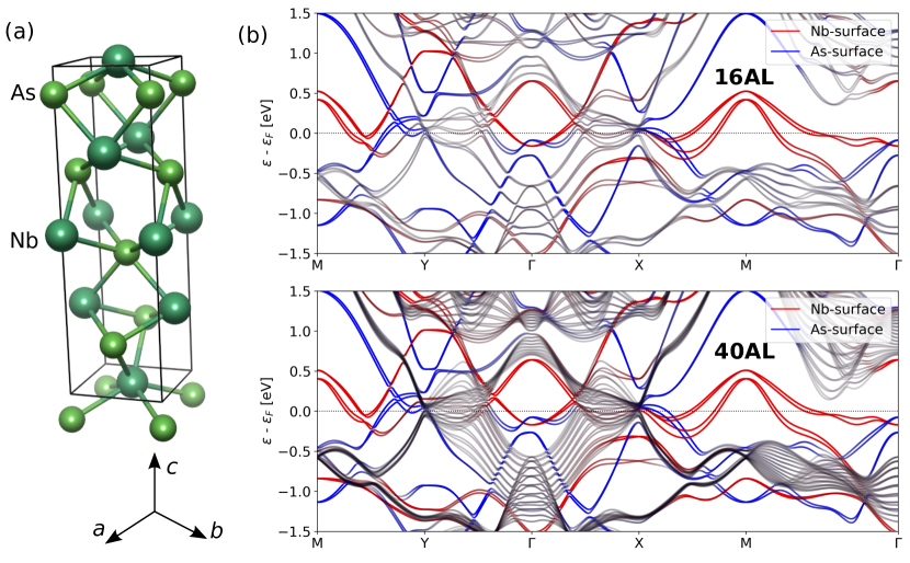
Bandstructure and Fermi surface: Figure 1(b) shows the first-principles-computed bandstructures of 16 atomic-layer (AL) () and 40 AL () (001) slabs of NbAs. The colors represent the contribution of spatial regions to each electronic state: bulk in gray, Nb-terminated surface in red and As-terminated surface in blue. Increasing the thickness of the slabs (16 AL 40 AL) increases the number of bulk bands but the surface bands remain largely unchanged. Note that the (001) surface of NbAs reduces the rotational symmetry of the bulk to 1, 49. As a result, both the Nb-terminated (red) and As-terminated (blue) surface bands differ between the -X and -Y high-symmetry -point paths. The bulk (gray) bands, which dominate the Y--X path, however, are mostly symmetric about . At the Fermi level, the Nb-terminated surface bands are hole-like along X--Y and electron-like along M-Y--X. These results agree with previous DFT bandstructure calculations for NbAs films 49.
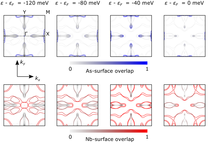
Next, we analyze the Fermi surfaces of (001) NbAs slabs to get insight into its electronic bandstructure. Since electronic states at the Fermi level dominate conduction, we aim to find the chemical potential at which the DFT-predicted isoenergy surfaces agree the best with ARPES data 4 to use for subsequent non-equilibrium Green’s function (NEGF) calculations. Figure 2 shows the isoenergy surfaces for a 56 AL slab computed using the Wannierized electronic states (-point grid: at different energy levels near the neutral Fermi level , with meV. As described in the Methods section, these isoenergy surfaces have been resolved by contributions of the bulk (gray), Nb-terminated (red) and As-terminated (blue) surfaces.
Comparing the top and bottom rows, we find that a disproportionate number of states belong to the Nb-terminated surface. Sun et al. 49 noted that strong hybridization between the surface and bulk states, and between trivial Fermi surfaces and arcs, makes it difficult to isolate the topological Fermi-arc states. However, careful analysis of spin textures 49 and ARPES measurements 4 has indicated that the outer arc of the spoon-shaped features along -X and -Y are the Fermi arcs. These arcs are not clearly visible at the DFT-predicted Fermi level , but become clearer with decreasing and achieve good agreement with the ARPES measurements of the As-terminated surface at meV. Hence, we shift the Fermi level down by 80 meV from the original DFT-computed value for all transport predictions reported below.
Ballistic conductance scaling: We first compute the ballistic conductance of pristine films of NbAs as a function of thickness using
| (1) |
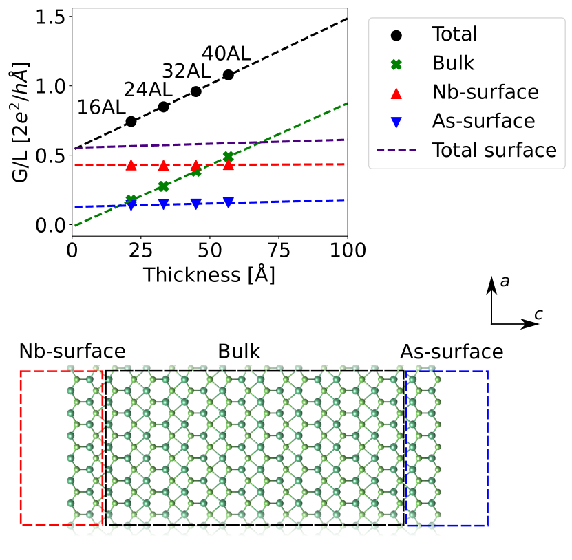
where and are the electronic energies and velocities of band and wavevector in the Brillouin zone (BZ) and is the spin degeneracy factor ( for the vs. relations with spin-orbit coupling). The derivative of the Fermi-Dirac occupations limits the contributions of electronic states to within a few around the Fermi level (Refer SI for a detailed derivation of Equation 1). We evaluate the above expression in JDFTx 50 for room temperature ( eV) using a Monte Carlo sampling of 250,000 -points in the BZ. We also decompose the total conductance into contributions from bulk, Nb-terminated and As-terminated surfaces by weighing each electronic state in the integrand of Eq. 1 with a slab weight function described in the Methods sections. The bounding box or slab used to define the spatial region for the surface states has been show in Figure 3.
We see that the total ballistic conductance per unit length () increases linearly with thickness (Figure 3). The decomposition of the total conductance into bulk and surface contributions shows that the Nb- and As-terminated surface-state contributions remain constant with thickness. The bulk conductance contribution decreases linearly with decrease in film thickness and extrapolates to nearly zero for zero thickness. Hence, the total conductance can be expressed as
| (2) |
where is the thickness of the film, is the slope of the linear fit to bulk conductance and and are the conductance due to Nb- and As-terminated surfaces respectively. For a 16 AL ( 2.1 nm) slab, the surface states and bulk account for and of the total ballistic conductance respectively. Such large surface state contributions to conductance have been observed for other topological semimetals as well, e.g. surface-state contribution in 2.7-nm-thick CoSi 47. As we increase the thickness to 40 AL ( 5.7 nm), the bulk conductance contribution for NbAs increases to while the surface contribution reduces to . Extrapolation of the linear fits to bulk and total surface conductance () reveals that the crossover point where surface and bulk conductance become equal is at around 6.8 nm which corresponds to a relaxed 48 AL slab. We also find that due to the larger number of states at the Fermi level, the ballistic conductance of NbAs (001) films is larger than that of CoSi (See Figure S7). Specifically, for a 2.5-nm-thick slab, the conductance for NbAs is around higher than that of CoSi
Importantly, the Nb-terminated surface contributes almost 3 times as much as the As-terminated surface to ballistic conductance, i.e., . This is in line with the Nb-terminated surface states vastly outnumbering the As-terminated surface states in the surface-resolved Fermi surfaces shown in Figure 2.
Note that shifting the boundary of the bounding box/slab further into the slab (Figure 3) would count more electronic states as surface states, including a part of the bulk conductance into the surface. While the definition of these boundaries is arbitrary, we have chosen it to the maximum value for which remains thickness independent in order to capture as much of the surface state contribution as possible, without including the bulk.
Resistance-area product scaling: We next analyze the resistance-area () product scaling for films of NbAs with and without defects (pristine) and compare the results with those of Cu (a conventional metal) and CoSi (a chiral multifermion semimetal) (Figure 4(a)). The resistance of these films have been calculated using the transmission at the Fermi level using
| (3) |
Here, is the quantum of conductance . The transmission is computed using the NEGF method 51, where we employ Wannier tight-binding Hamiltonians constructed using DFT as described in the Methods section.
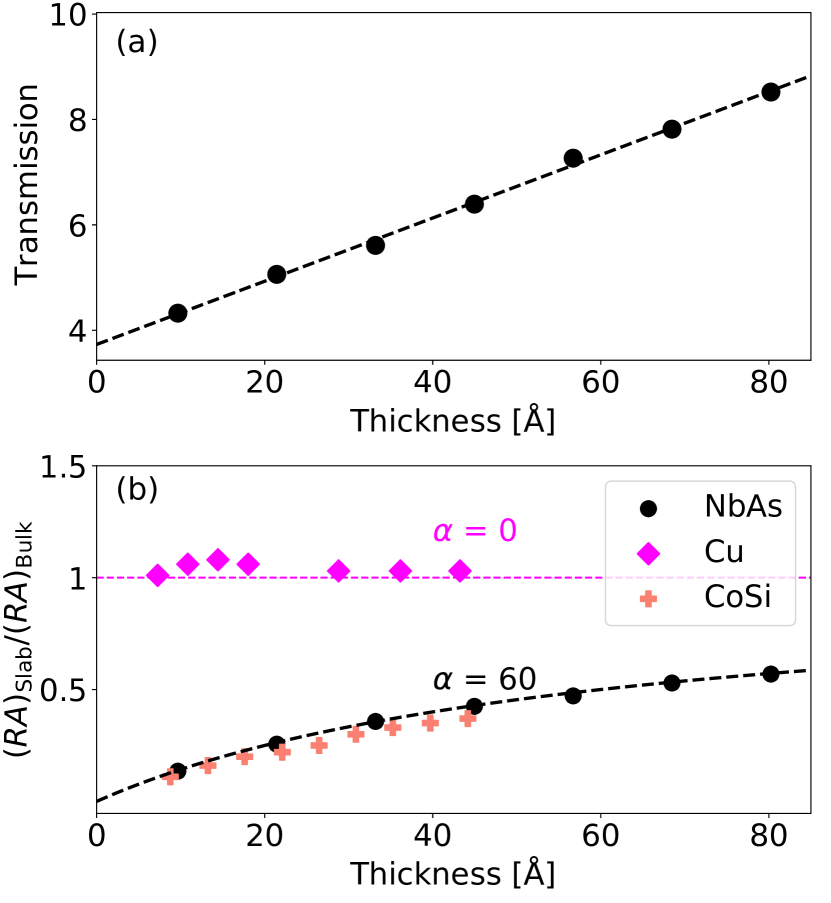
Previous first-principles NEGF calculations have shown that the product of slabs for pristine Cu is mostly independent of slab thickness 52, 14, 47, because bulk states dominate conduction. A similar trend has also been observed for MoP, a topological metal, where most of the electronic states at the Fermi level are bulk states 46. Hence, for such materials, conductance decreases linearly with decreasing thickness or cross-sectional area , making the product constant. Consequently, independent of film thickness, the normalized product .
In contrast, NEGF calculations of pristine films of NbAs show that decreases with decreasing film thickness and is always less than , similar to previous reports for CoSi films 14, 47. This can be explained by extending Equation 2 to calculate
| (4) |
where . (See SI for derivation.) Equation 4 predicts that in pristine slabs of any finite thickness , as long as there is some surface contribution, . When surface conductance is negligible, leading to , we find normalized for all thicknesses, exactly as observed for conventional metals such as Cu. Figure 4(b) shows an excellent fit of the computed with Equation 4, establishing the validity of the simple model of additive surface and bulk conductance for Weyl semimetals.
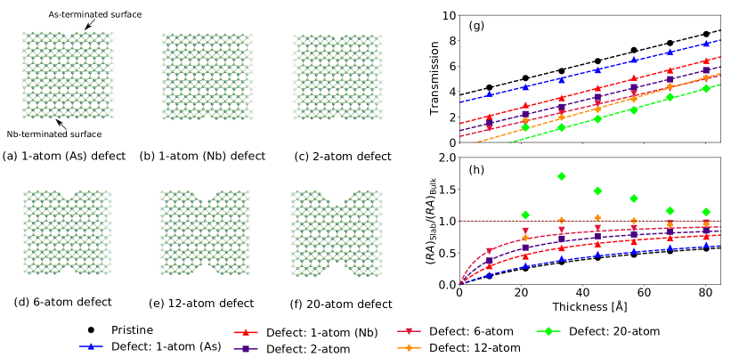
We now investigate the effect of notches or surface line-defects on the ballistic conductance of NbAs films. We study six different types of defects as shown in Figure 5(a-f). The calculated transmission and the resultant normalized product are shown in Figures 5(g) and (h) respectively. As expected, the transmission for pristine films increases linearly with thickness, which corresponds to the increasing number of bulk conducting channels/bands at the Fermi level. We perform a linear fit () for the thickness-dependent transmission data for all defect types. (The parameters slope , intercept and have been provided in Table S1.) Removing an As atom from the As-terminated (top) surface leads to a relatively small drop in the transmission for all the slabs, such that the intercept of the linear fit drops only slightly, . However, removing a Nb atom from the Nb-terminated (bottom) surface causes an almost 4 times larger reduction () in the transmission. For the third case (Figure 5(c)), where we remove an atom each from the top and bottom surface, the transmission reduces by , which is equal to the sum of the above two reductions. As we increase the depth of the ‘notch’ on the surfaces (Figure 5(d-f)), the net transmission continues to diminish. We note that the total transmission extrapolated to zero thickness remains finite in films with single-atom, 2-atom, and 6-atom line-defects, indicative of the survival of surface-state conduction in films with sufficiently small disorder. With the deep 12-atom and 20-atom defects, the transmission reduction levels off for the thinnest film and leads to the downturn in the product with scaling as shown in Figure 5(h). This is similar to the resistivity scaling trend reported previously for CoSi films with high surface defect densities 47.
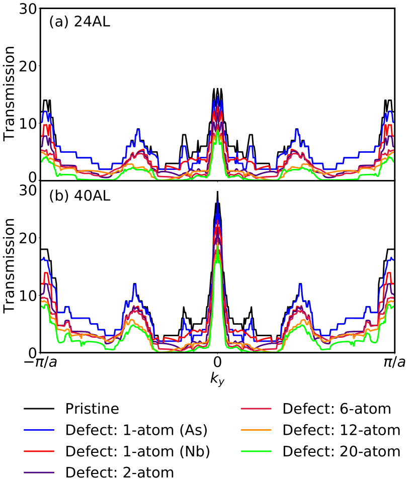
To further understand the above observations, we analyze the -resolved transmission for two representative cases of 24AL and 40AL slabs. Figure 6 shows the transmission plotted against direction which is the in-plane direction normal to the transport direction . Since the transmission for pristine films essentially represents the number of states at the Fermi level, the values are integers for any . As the thickness increases, we see an increase in the peak heights around , , and corresponding to the increasing number of bulk states around those points in the Brillouin Zone. (See Figure S6 in SI). In general, defects reduce the transmission, though by varying degree as noted in Figure 5(g). The 1-atom defect on the As-terminated surface negligibly changes the transmission for and , because there are no surface states on the As-terminated surface in that region (Figure S6). Consequently, the localization of As-terminated surface states in the -space leads to the small overall change in transmission. Most of the surface states at the Fermi level that contribute to conduction exist on the Nb-terminated surface, as shown previously in Figure 3. Correspondingly, a defect on the Nb-terminated surface considerably reduces the transmission throughout , since the Nb-terminated states extend throughout the projected 2D Brillouin Zone. The 2-atom defect, removing one Nb and one As atom on each surface, reduces the transmission by roughly the sum of the previous two cases. We find the transmission reduces further for every point along for 6-atom, 12-atom and 20-atom defects.
Using the net transmission calculated above, we plot the normalized product in Figure 5(h) for the various defect configurations. Since the transmission continues to exhibit a roughly linear dependence on thickness for the cases with defects, we could employ a model similar to Equation 4 to fit the computed data. Specifically, we write . Comparing to Equation 4, we note that . We find that the normalized product for the first four defect types exhibit a trend similar to the pristine case, i.e. decreases with decreasing thickness. Since the net transmission doesn’t change significantly for the 1-atom defect on the As-terminated surface, its normalized curve (blue) is very close to the case with no defects (black) in Figure 5(h). Increasing the size of the defects makes the vs. curves flatter, as the normalized product begins to become thickness independent and approaches 1 when the surface state conduction gradually diminishes, manifested in the intercept of transmission approaching zero. Thus, in the limit of sufficiently strong surface disorder, the Weyl semimetal behaves more like a conventional metal in this respect. For example, the 12-atom and 20-atom defect configurations begin to kill the transmission of the bulk states besides significantly suppressing surface conduction, which makes the product of the slab greater than that of the ideal bulk.
Importantly, for very thin films, the 12-atom and 20-atom defect configurations are large enough to significantly perturb the electronic states in the region near the defect. In our current approach, however, the tight-binding models are based on the ground state of the pristine films, and the couplings linked to the removed atom are deleted to mimic the defect. Therefore, the calculated transmissions at 16 AL and below for these two defect configurations are likely to be less reliable than the remaining cases. Although more accurate results can be obtained using self-consistent DFT and NEGF in QuantumATK 53, it can be computationally expensive and potentially prohibitive for large-thickness structures with spin-orbit coupling, as studied here. Nevertheless, the qualitative trend discussed above that the transmission levels off in the ultra-thin film limit is also demonstrated by the fully self-consistent DFT with NEGF calculations using QuantumATK 53 (Figure S1).
Finally, we compare the conductance scaling of NbAs films with that of CoSi. Both materials show decreasing with reduced thickness in pristine films, owing to the dominance of surface conduction over bulk conduction at the nanometer scale. However, CoSi is a chiral semimetal with forward- and backward-moving surface carriers from the Fermi-arc states of the same transverse momentum spatially separated on opposite surfaces of a CoSi thin film 14. Consequently, line defects which preserve the transverse momentum cannot backscatter these states into each other and the transmission of the CoSi Fermi arc states is robust against such defects 14. In contrast, the forward- and backward-moving surface carriers with the same transverse momentum coexist on both surfaces of NbAs, and thus can intermix (See Figure S8). Therefore, transmission of the NbAs Fermi-arc states is much more susceptible to defect scattering. As shown in Figure 6, a line-defect can reduce the transmission for all -points in the Brillouin zone, contrary to that in the CoSi films. This explains the substantial reduction of total transmission in NbAs films with single-atom defects (see Figure 5). Experimentally, the 2-3 orders of magnitude increase in resistivity observed in 600 nm diameter NbAs nanowires 4 when compared to the micron-size wide nanobelts also demonstrates the sensitivity of the NbAs surface states to defect scattering at the boundaries. Therefore, for materials with optimal disorder-tolerant surface-state conductivity, future work should explore chiral topological semimetals with multiple pairs of Weyl nodes.
3 Conclusions
In summary, we performed first-principles NEGF calculations to understand the mechanism of electron transport in thin films of a representative Weyl semimetal, NbAs. The resistance-area product in pristine NbAs films decreases with thickness at the nanometer scale, in contrast to a nearly constant product in ideal Cu films. This anomalous scaling is the manifestation of the numerous surface states in the bandstructure of NbAs. The surface states account for over 70 of the conductance for 2.1-nm-thick (relaxed 16 AL) films and 50 for 6.8-nm-thick (relaxed 48 AL) films; furthermore, contribution from the Nb-terminated surface states is almost 3 times that of the As-terminated-surface states. The decreasing with reducing dimensions persists even with surface defects, as long as the degree of disorder is moderate. This contrasts the ever increasing with reducing dimensions in conventional metals like Cu when disorder is present, and highlights the promise of Weyl semimetal NbAs, and topological semimetals in general, for integrated circuits. Finally, analyses of electron transmission in -space show that electron transport in NbAs is not immune to defect scattering because forward- and backward-moving states coexist on the same surface, in contrast to the protected chiral surface transport in CoSi thin films. The comparison between the two material systems calls for the search for chiral topological semimetals with large numbers of Fermi arcs for low-resistance nanoscale interconnects.
4 Methods
We use open-source plane-wave DFT software JDFTx 50 for the generation of self-consistent relaxed crystal structures, electron bandstructures and Wannier tight-binding models. We use the fully-relativistic optimized norm-conserving Vanderbilt pseudopotentials (ONCVPSP) 54 as distributed by the open-source PSEUDODOJO library 55 to include spin-orbit coupling self-consistently. These DFT calculations are performed using the Perdew-Burke-Ernzerhof (PBE) generalized gradient approximation (GGA) to the exchange-correlation functional 56 at a plane-wave cutoff of 40 Hartrees and a charge density cutoff of 200 Hartrees.
For the first-principles study of NbAs slabs, we construct films of (001) orientation to allow direct comparison of our computed Fermi surfaces with the available ARPES results, which have been experimentally measured for the cleaved (001) surfaces 1, 49. These slabs have tetragonal unit cells, and are constructed with a vacuum spacing of thickness along the direction, employing Coulomb truncation to eliminate long-range interactions between periodic images along this direction 57, 58, 59. Cleaving the surface along (001) direction leads to two asymmetric surfaces with Nb and As terminations respectively (Figure 1(a)), which produces an overall dipole moment in the unit cell. Figure S2 shows that the Coulomb truncation scheme accounts for this dipole correctly and produces zero electric field in the vacuum region away from both surfaces.
With the computational setup described above, we first perform an optimization of the ionic positions and lattice parameters of the body-centered tetragonal unit cell of bulk NbAs (space group ). The initial crystal structure was obtained from the Materials Project database 60. The relaxation yields lattice constants of and which are within 1% of the XRD measured values of and (Figure 1(a)) 1, 61. Starting from a single-unit-cell thick slab, we then construct films with seven different thicknesses in steps of 1 unit cell. Hence, the thickness of our films vary from 1 unit cell or 8 atomic layers (AL) to 7 unit cells or 56 atomic layers (AL). Previous first-principles calculations for NbAs have found no noticeable change in the band structure and Fermi surfaces for slabs larger than 7 unit cells in thickness 49. The DFT calculations for the bulk and slabs are performed using k-point meshes of and respectively, and Fermi smearing with width 0.01 Hartrees. Keeping the in-plane lattice constants of the slabs fixed (), we optimize the ionic positions using self-consistent DFT for subsequent calculations of electronic bands, Fermi surface and electron transport properties.
We then construct a tight-binding model using a maximally-localized Wannier function basis set 62 in JDFTx. Figure S3 shows the contribution of , and orbitals of Nb and As atoms to each band for a 16AL slab. The electron bands in the energy range eV around the Fermi level are mostly composed of the and orbitals of Nb and As atoms respectively. Hence, we choose a basis set of 10 orbitals per Nb atom and 6 orbitals per As atom in the unit cell as the initial guesses. We construct maximally-localized Wannier functions for our ab initio tight-binding model that reproduces the DFT bands in the energy window of eV to eV above , as shown in Figure S4.
To pinpoint the contributions of surface and bulk contributions to the band structure, Fermi surfaces and conductance in the Wannier basis, we compute weights of each Wannier-interpolated electronic state from the surface regions. Specifically, we define functions for = Nb and As, which are 1 within the dashed rectangles shown in the bottom panel of Fig. 3, and 0 outside it. We then compute the matrix elements (), where is smoothed by convolution with a Gaussian of width 1 bohr. Finally, we interpolate using the Wannier representation in exactly the same way as the Hamiltonian and momentum matrix elements described in detail elsewhere 63, 64.
Using the tight-binding models created above, we employ Non-equilibrium Green’s Function (NEGF) method to compute the electron transport properties of the films 51. For the slab of NbAs, we consider transport along the [100] direction and calculate the total transmission as
| (5) |
where is the -resolved transmission and is the in-plane direction. Here, is the retarded Green’s function, is the tight-binding Hamiltonian of channel, and is the contact self-energy of the left and right contact. is the advanced Green’s function, and is the broadening of the contact- . The contact self-energies are numerically solved using the Sancho-Rubio’s method 65. For the bulk of NbAs, similarly, the transmission can be written as
| (6) |
where the is the out-of-plane direction for the bulk. We use -point sampling of and for slab and bulk transport calculation, respectively. The Hamiltonian of the channel is constructed from the slab tight-binding model. In order to consider surface defect configurations in the channel, we remove the orbitals of atoms entirely from the Hamiltonian of channel . Figure S5 shows the schematic view of structure for NEGF calculation for 24AL slab of NbAs with 12-atom defect configuration.
5 Acknowledgements
S.K and R.S. acknowledge funding from Semiconductor Research Corporation under Task No. 2966.002. Calculations were carried out at the Center for Computational Innovations at Rensselaer Polytechnic Institute. The work at the National University of Singapore was supported by MOE-2017-T2-2-114, MOE-2019-T2-2-215, and FRC-A-8000194-01-00. T.-R.C. was supported by 2030 Cross-Generation Young Scholars Program from the National Science and Technology Council (NSTC) in Taiwan (MOST111-2628-M-006-003-MY3), National Cheng Kung University, Taiwan, and the National Center for Theoretical Sciences, Taiwan. We gratefully acknowledge the helpful discussions with Daniel Gall (RPI), Utkarsh Bajpai (IBM) and Vijay Narayanan (IBM).
References
- Xu et al. 2015 Xu, S.-Y.; Belopolski, I.; Alidoust, N.; Neupane, M.; Bian, G.; Zhang, C.; Sankar, R.; Chang, G.; Yuan, Z.; Lee, C.-C., et al. Discovery of a Weyl fermion semimetal and topological Fermi arcs. Science 2015, 349, 613–617
- Yang et al. 2015 Yang, L.; Liu, Z.; Sun, Y.; Peng, H.; Yang, H.; Zhang, T.; Zhou, B.; Zhang, Y.; Guo, Y.; Rahn, M., et al. Weyl semimetal phase in the non-centrosymmetric compound TaAs. Nature physics 2015, 11, 728–732
- Lv et al. 2015 Lv, B.; Weng, H.; Fu, B.; Wang, X. P.; Miao, H.; Ma, J.; Richard, P.; Huang, X.; Zhao, L.; Chen, G., et al. Experimental discovery of Weyl semimetal TaAs. Physical Review X 2015, 5, 031013
- Xu et al. 2015 Xu, S.-Y.; Alidoust, N.; Belopolski, I.; Yuan, Z.; Bian, G.; Chang, T.-R.; Zheng, H.; Strocov, V. N.; Sanchez, D. S.; Chang, G., et al. Discovery of a Weyl fermion state with Fermi arcs in niobium arsenide. Nature Physics 2015, 11, 748–754
- Armitage et al. 2018 Armitage, N.; Mele, E.; Vishwanath, A. Weyl and Dirac semimetals in three-dimensional solids. Reviews of Modern Physics 2018, 90, 015001
- Lv et al. 2021 Lv, B.; Qian, T.; Ding, H. Experimental perspective on three-dimensional topological semimetals. Reviews of Modern Physics 2021, 93, 025002
- Hasan et al. 2021 Hasan, M. Z.; Chang, G.; Belopolski, I.; Bian, G.; Xu, S.-Y.; Yin, J.-X. Weyl, Dirac and high-fold chiral fermions in topological quantum matter. Nature Reviews Materials 2021, 6, 784–803
- Yan and Felser 2017 Yan, B.; Felser, C. Topological materials: Weyl semimetals. Annual Review of Condensed Matter Physics 2017, 8, 337–354
- Bansil et al. 2016 Bansil, A.; Lin, H.; Das, T. Colloquium: Topological band theory. Reviews of Modern Physics 2016, 88, 021004
- Wu et al. 2017 Wu, L.; Patankar, S.; Morimoto, T.; Nair, N. L.; Thewalt, E.; Little, A.; Analytis, J. G.; Moore, J. E.; Orenstein, J. Giant anisotropic nonlinear optical response in transition metal monopnictide Weyl semimetals. Nature Physics 2017, 13, 350–355
- Han et al. 2021 Han, J.; McGoldrick, B. C.; Chou, C.-T.; Safi, T. S.; Hou, J. T.; Liu, L. Current-induced switching of a ferromagnetic Weyl semimetal Co2MnGa. Applied Physics Letters 2021, 119, 212409
- De Sousa et al. 2021 De Sousa, D.; Ascencio, C.; Haney, P. M.; Wang, J.-P.; Low, T. Gigantic tunneling magnetoresistance in magnetic Weyl semimetal tunnel junctions. Physical Review B 2021, 104, L041401
- Osterhoudt et al. 2019 Osterhoudt, G. B.; Diebel, L. K.; Gray, M. J.; Yang, X.; Stanco, J.; Huang, X.; Shen, B.; Ni, N.; Moll, P. J.; Ran, Y., et al. Colossal mid-infrared bulk photovoltaic effect in a type-I Weyl semimetal. Nature materials 2019, 18, 471–475
- Chen et al. 2020 Chen, C.-T.; Bajpai, U.; Lanzillo, N. A.; Hsu, C.-H.; Lin, H.; Liang, G. Topological Semimetals for Scaled Back-End-Of-Line Interconnect Beyond Cu. 2020 IEEE International Electron Devices Meeting (IEDM). 2020; pp 32–4
- Han et al. 2021 Han, H. J.; Liu, P.; Cha, J. J. 1D topological systems for next-generation electronics. Matter 2021, 4, 2596–2598
- Gall et al. 2021 Gall, D.; Cha, J. J.; Chen, Z.; Han, H.-J.; Hinkle, C.; Robinson, J. A.; Sundararaman, R.; Torsi, R. Materials for interconnects. MRS Bulletin 2021, 1–8
- Lanzillo et al. 2022 Lanzillo, N. A.; Bajpai, U.; Garate, I.; Chen, C.-T. Size-Dependent Grain-Boundary Scattering in Topological Semimetals. Physical Review Applied 2022, 18, 034053
- Nagaosa et al. 2020 Nagaosa, N.; Morimoto, T.; Tokura, Y. Transport, magnetic and optical properties of Weyl materials. Nature Reviews Materials 2020, 5, 621–636
- Hu et al. 2019 Hu, J.; Xu, S.-Y.; Ni, N.; Mao, Z. Transport of Topological Semimetals. Annual Review of Materials Research 2019, 49, 207–252
- Wang et al. 2017 Wang, S.; Lin, B.-C.; Wang, A.-Q.; Yu, D.-P.; Liao, Z.-M. Quantum transport in Dirac and Weyl semimetals: a review. Advances in Physics: X 2017, 2, 518–544
- Gorbar et al. 2018 Gorbar, E.; Miransky, V.; Shovkovy, I.; Sukhachov, P. Anomalous transport properties of Dirac and Weyl semimetals. Low Temperature Physics 2018, 44, 487–505
- Ong and Liang 2021 Ong, N.; Liang, S. Experimental signatures of the chiral anomaly in Dirac–Weyl semimetals. Nature Reviews Physics 2021, 3, 394–404
- Sodemann and Fu 2015 Sodemann, I.; Fu, L. Quantum nonlinear Hall effect induced by Berry curvature dipole in time-reversal invariant materials. Physical review letters 2015, 115, 216806
- Ma et al. 2019 Ma, Q.; Xu, S.-Y.; Shen, H.; MacNeill, D.; Fatemi, V.; Chang, T.-R.; Mier Valdivia, A. M.; Wu, S.; Du, Z.; Hsu, C.-H., et al. Observation of the nonlinear Hall effect under time-reversal-symmetric conditions. Nature 2019, 565, 337–342
- Kang et al. 2019 Kang, K.; Li, T.; Sohn, E.; Shan, J.; Mak, K. F. Nonlinear anomalous Hall effect in few-layer WTe2. Nature materials 2019, 18, 324–328
- de Juan et al. 2017 de Juan, F.; Grushin, A. G.; Morimoto, T.; Moore, J. E. Quantized circular photogalvanic effect in Weyl semimetals. Nature communications 2017, 8, 1–7
- Rees et al. 2020 Rees, D.; Manna, K.; Lu, B.; Morimoto, T.; Borrmann, H.; Felser, C.; Moore, J.; Torchinsky, D. H.; Orenstein, J. Helicity-dependent photocurrents in the chiral Weyl semimetal RhSi. Science advances 2020, 6, eaba0509
- Ni et al. 2021 Ni, Z.; Wang, K.; Zhang, Y.; Pozo, O.; Xu, B.; Han, X.; Manna, K.; Paglione, J.; Felser, C.; Grushin, A. G., et al. Giant topological longitudinal circular photo-galvanic effect in the chiral multifold semimetal CoSi. Nature communications 2021, 12, 1–8
- Patankar et al. 2018 Patankar, S.; Wu, L.; Lu, B.; Rai, M.; Tran, J. D.; Morimoto, T.; Parker, D. E.; Grushin, A. G.; Nair, N.; Analytis, J., et al. Resonance-enhanced optical nonlinearity in the Weyl semimetal TaAs. Physical Review B 2018, 98, 165113
- Breitkreiz and Brouwer 2019 Breitkreiz, M.; Brouwer, P. W. Large contribution of Fermi arcs to the conductivity of topological metals. Physical review letters 2019, 123, 066804
- Resta et al. 2018 Resta, G.; Pi, S.-T.; Wan, X.; Savrasov, S. Y. High surface conductivity of Fermi-arc electrons in Weyl semimetals. Physical Review B 2018, 97, 085142
- Gorbar et al. 2016 Gorbar, E.; Miransky, V.; Shovkovy, I.; Sukhachov, P. Origin of dissipative Fermi arc transport in Weyl semimetals. Physical Review B 2016, 93, 235127
- Wilson et al. 2018 Wilson, J. H.; Pixley, J.; Huse, D. A.; Refael, G.; Sarma, S. D. Do the surface Fermi arcs in Weyl semimetals survive disorder? Physical Review B 2018, 97, 235108
- Fuchs 1938 Fuchs, K. Math. Proc. Cambridge Philos. Soc. 1938
- Sondheimer 1952 Sondheimer, E. Adv. Phys. 1952
- Mayadas et al. 1969 Mayadas, A.; Shatzkes, M.; Janak, J. Electrical resistivity model for polycrystalline films: the case of specular reflection at external surfaces. Applied Physics Letters 1969, 14, 345–347
- Mayadas and Shatzkes 1970 Mayadas, A.; Shatzkes, M. Electrical-resistivity model for polycrystalline films: the case of arbitrary reflection at external surfaces. Physical review B 1970, 1, 1382
- Gall 2020 Gall, D. The search for the most conductive metal for narrow interconnect lines. Journal of Applied Physics 2020, 127, 050901
- Soulié et al. 2021 Soulié, J.-P.; Tőkei, Z.; Swerts, J.; Adelmann, C. Aluminide intermetallics for advanced interconnect metallization: thin film studies. 2021 IEEE International Interconnect Technology Conference (IITC). 2021; pp 1–3
- Chen et al. 2018 Chen, L.; Ando, D.; Sutou, Y.; Gall, D.; Koike, J. NiAl as a potential material for liner-and barrier-free interconnect in ultrasmall technology node. Applied Physics Letters 2018, 113, 183503
- Chen et al. 2021 Chen, L.; Kumar, S.; Yahagi, M.; Ando, D.; Sutou, Y.; Gall, D.; Sundararaman, R.; Koike, J. Interdiffusion reliability and resistivity scaling of intermetallic compounds as advanced interconnect materials. Journal of Applied Physics 2021, 129, 035301
- Zhang and Gall 2022 Zhang, M.; Gall, D. Resistivity Scaling in Epitaxial CuAl 2 (001) Layers. IEEE Transactions on Electron Devices 2022, 69, 5110–5115
- Sankaran et al. 2020 Sankaran, K.; Moors, K.; Tőkei, Z.; Adelmann, C.; Pourtois, G. Ab initio screening of metallic MAX ceramics for advanced interconnect applications. arXiv preprint arXiv:2011.06902 2020,
- Zhang et al. 2021 Zhang, M.; Kumar, S.; Sundararaman, R.; Gall, D. Resistivity scaling in epitaxial MAX-phase Ti4SiC3 (0001) layers. Journal of Applied Physics 2021, 130, 034302
- Kumar et al. 2022 Kumar, S.; Multunas, C.; Defay, B.; Gall, D.; Sundararaman, R. Ultralow electron-surface scattering in nanoscale metals leveraging Fermi-surface anisotropy. Phys. Rev. Materials 2022, 6, 085002
- Han et al. 2022 Han, H. J.; Kumar, S.; Ji, X.; Hart, J. L.; Jin, G.; Hynek, D. J.; Sam, Q. P.; Hasse, V.; Felser, C.; Cahill, D. G., et al. Topological Metal MoP Nanowire for Interconnect. arXiv preprint arXiv:2208.02784 2022,
- Lien et al. 2022 Lien, S.-W.; Garate, I.; Bajpai, U.; Huang, C.-Y.; Hsu, C.-H.; Tu, Y.-H.; Lanzillo, N. A.; Bansil, A.; Chang, T.-R.; Liang, G., et al. Unconventional Resistivity Scaling in Topological Semimetal CoSi. arXiv preprint arXiv:2209.06135 2022,
- Zhang et al. 2019 Zhang, C.; Ni, Z.; Zhang, J.; Yuan, X.; Liu, Y.; Zou, Y.; Liao, Z.; Du, Y.; Narayan, A.; Zhang, H., et al. Ultrahigh conductivity in Weyl semimetal NbAs nanobelts. Nature materials 2019, 18, 482–488
- Sun et al. 2015 Sun, Y.; Wu, S.-C.; Yan, B. Topological surface states and Fermi arcs of the noncentrosymmetric Weyl semimetals TaAs, TaP, NbAs, and NbP. Physical Review B 2015, 92, 115428
- Sundararaman et al. 2017 Sundararaman, R.; Letchworth-Weaver, K.; Schwarz, K.; Gunceler, D.; Ozhabes, Y.; Arias, T. A. JDFTx: Software for joint density-functional theory. SoftwareX 2017, 6, 278 – 284
- Datta 2005 Datta, S. Quantum transport: atom to transistor; Cambridge university press, 2005
- Timoshevskii et al. 2008 Timoshevskii, V.; Ke, Y.; Guo, H.; Gall, D. The influence of surface roughness on electrical conductance of thin Cu films: An ab initio study. Journal of Applied Physics 2008, 103, 113705
- Smidstrup et al. 2020 Smidstrup, S.; Markussen, T.; Vancraeyveld, P.; Wellendorff, J.; Schneider, J.; Gunst, T.; Verstichel, B.; Stradi, D.; Khomyakov, P. A.; Vej-Hansen, U. G., et al. QuantumATK: An integrated platform of electronic and atomic-scale modelling tools. J. Phys: Condens. Matter 2020, 32, 015901
- Hamann 2013 Hamann, D. Optimized norm-conserving Vanderbilt pseudopotentials. Physical Review B 2013, 88, 085117
- van Setten et al. 2018 van Setten, M. J.; Giantomassi, M.; Bousquet, E.; Verstraete, M. J.; Hamann, D. R.; Gonze, X.; Rignanese, G.-M. The PseudoDojo: Training and grading a 85 element optimized norm-conserving pseudopotential table. Computer Physics Communications 2018, 226, 39–54
- Perdew et al. 1996 Perdew, J. P.; Burke, K.; Ernzerhof, M. Phys. Rev. Lett. 1996, 77, 3865
- Sundararaman and Arias 2013 Sundararaman, R.; Arias, T. Regularization of the Coulomb singularity in exact exchange by Wigner-Seitz truncated interactions: Towards chemical accuracy in nontrivial systems. Physical Review B 2013, 87, 165122
- Ismail-Beigi 2006 Ismail-Beigi, S. Truncation of periodic image interactions for confined systems. Physical Review B 2006, 73, 233103
- Rozzi et al. 2006 Rozzi, C. A.; Varsano, D.; Marini, A.; Gross, E. K.; Rubio, A. Exact Coulomb cutoff technique for supercell calculations. Physical Review B 2006, 73, 205119
- Jain et al. 2013 Jain, A.; Ong, S. P.; Hautier, G.; Chen, W.; Richards, W. D.; Dacek, S.; Cholia, S.; Gunter, D.; Skinner, D.; Ceder, G.; Persson, K. a. The Materials Project: A materials genome approach to accelerating materials innovation. APL Materials 2013, 1, 011002
- Boller and Parthé 1963 Boller, H.; Parthé, E. The transposition structure of NbAs and of similar monophosphides and arsenides of niobium and tantalum. Acta Crystallographica 1963, 16, 1095–1101
- Marzari et al. 2012 Marzari, N.; Mostofi, A. A.; Yates, J. R.; Souza, I.; Vanderbilt, D. Maximally localized Wannier functions: Theory and applications. Rev. Mod. Phys. 2012, 84, 1419–1475
- Habib et al. 2018 Habib, A.; Florio, F.; Sundararaman, R. Hot carrier dynamics in plasmonic transition metal nitrides. Journal of Optics 2018, 20, 064001
- Kumar et al. 2022 Kumar, S.; Multunas, C.; Sundararaman, R. Plasmonic hot carrier dynamics in directional conductors. arXiv preprint arXiv:2205.05007 2022,
- Sancho et al. 1984 Sancho, M. L.; Sancho, J. L.; Rubio, J. Quick iterative scheme for the calculation of transfer matrices: application to Mo (100). Journal of Physics F: Metal Physics 1984, 14, 1205