Probing the Atomic Arrangement of Sub-Surface Dopants in a Silicon Quantum Device Platform
Abstract
High-density structures of sub-surface phosphorus dopants in silicon continue to garner interest as a silicon-based quantum computer platform, however, a much-needed confirmation of their dopant arrangement has been lacking. In this work, we take advantage of the chemical specificity of X-ray photoelectron diffraction to obtain the precise structural configuration of \ceP dopants in sub-surface Si:P -layers. The growth of -layer systems with different levels of doping is carefully studied and verified using X-ray photoelectron spectroscopy and low-energy electron diffraction. Subsequent XPD measurements reveal that in all cases, the dopants primarily substitute with Si atoms from the host material. Furthermore, no signs of free carrier-inhibiting PP dimerization can be observed. Our observations not only settle a nearly decade-long debate about the dopant arrangement but also demonstrate that XPD is well suited to study sub-surface dopant structures. This work thus provides valuable input for an updated understanding of the behavior of Si:P -layers and the modeling of their derived quantum devices.
Introduction
Over the last decade, the effort to realize a silicon-based, CMOS-compatible quantum computer has been intensifying [1, 2, 3], and several significant breakthroughs have been achieved [4, 5, 6]. One common factor in this development is the so-called Si:P -layer platform [7, 8]; i.e. an ultra-sharp and narrow layer of phosphorus dopants placed beneath the silicon surface, which can be patterned with atomic precision [9]. The -layer platform can be used for quantum dots and tunnel barriers [10], metallic interconnects [11], and other key components required for quantum device engineering [1]. This, in turn, has required it to be thoroughly studied and understood [12, 13, 14, 15, 16, 17, 18, 19, 20, 21]. Despite these intense efforts and the great progress which has been made, one key question remains unanswered: What is the arrangement of the dopants within the -layer? The answer is of central importance for the performance of -layer-derived devices, because the dopant arrangement is understood to directly impact key electronic properties; for example, the energy separation (i.e. ‘valley-splitting’) of the supported quantum well states [22, 23, 24].
There may be multiple reasons why the atomic arrangement is not known, but we conjecture that it is primarily because, until now, a suitable probing method had not been identified. Traditional X-ray diffraction methods are unsuitable because of the atomically thin nature of the -layer [25]. High-angle annular dark-field imaging with an electron microscope is also exceptionally challenging, because of the similarity in atomic weight of Si and P [26]. Recent studies have shown that the quantum confinement of the -layer can be ascertained by means of ellipsometry [27], but the in-plane coordination of the dopants has remained elusive.
In this work, we demonstrate that the neighborhood around the dopants can be directly probed using X-ray photoelectron diffraction (XPD), in which a chemically specific diffractive image is formed by utilizing subtle core level energy shifts that are concomitant with the coordination of a dopant [28, 29]. Although XPD is primarily used as a probe of surface structure [30, 31, 32], we demonstrate here that it also has great potential for determining the local arrangement of sub-surface atoms and, therefore, is perfectly suited for solving the long-standing mystery of the Si:P -layer structure.
Results and Discussion
The growth of -layers has been studied and refined over the recent years, not least of all to maximize the density of P atoms within the dopant plane [33, 34]. The basic preparation approach involves exposing a clean Si(001) surface to a saturation coverage of \cePH3 gas, followed by subsequent dissociation of the gas and incorporation of P into the Si surface [35, 36, 37, 38]. Refinements of the method involving multiple cycles of \cePH3 exposure and \ceP incorporation have been shown to maximize the doping density, whilst retaining a sharp confinement of the -layer [34, 21]. In all cases, the doped surface is then overgrown with undoped silicon to encapsulate the dopant layer.
XPD, like other photoemission-based methods, is especially challenging to perform on buried atomic species because their resulting photoemission signal will be strongly attenuated by the overlayers [39]. This problem has been addressed previously, specifically for Si:P -layers [17, 40, 41]. In order to demonstrate that XPD is even possible, we therefore first focus on a -layer with a maximized dopant density (i.e. ‘double-dosed’), and with a minimized encapsulation layer thickness (i.e. ).
Quantitative X-ray photoelectron spectroscopy (XPS) analysis (see the Methods section) of the ‘double-dosed’ system before, during and after Si encapsulation reveals that a monolayer (ML) \ceP coverage is achieved, i.e. similar to the reported previously [34]. The same analysis also reveals that of the \ceP dopants remain in the -layer after the Si overlayer growth and final annealing steps have been completed (and the additional segregates to the surface). From our preparation we achieve an effective electron carrier density of (see the Methods section for details), in line with the best-case carrier density of for single-layer Si:P structures [34].
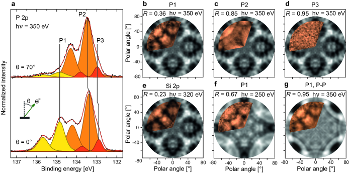
The XPS signal from the phosphorous core level, after the completion of all of the growth steps, is shown as Fig. 1a at two different emission angles (). The P 2p signal consists of three doublet components, each described by two Voigt functions with a spin-orbit splitting energy of and an intensity ratio of p3/2 : p. The doublet labelled P1 at largest binding energy () corresponds to the dopants in the buried Si:P -layer, whereas P2 () and P3 () correspond to surface phosphorus in two distinct co-ordinations [42]. Although of P is present in the buried layer, the strong attenuation of the photoemission signal from buried dopants makes P1 look very weak in comparison with the un-attenuated signal (P2, P3) from trace amounts of residual surface P.
To confirm the assignment of phosphorus components from the buried -layer and on the surface, the finite mean-free path () of photoelectrons can be exploited [39, 43]. The intensity of P1 relative to P2 and P3 is seen to be strongest at normal emission () but drastically reduced at . Assuming an intensity model , signals from dopants at a depth beneath the surface should attenuate more rapidly with increasing when compared to the surface species. From this argument, we confirm that P1 is located furthest away from the surface. Investigations as a function of the photoelectron kinetic energy lead to the same conclusion [42].
To determine their atomic arrangements both on and beneath the Si surface, XPD experiments of the P1-P3 components were performed. For this purpose, XPS measurements of P 2p were acquired over a large range of azimuthal () and polar () angles, and polar plots of its intensity modulation function were produced alongside corresponding diffraction simulations (see the Methods section).
Since the bulk structure of Si is known [44], the XPD pattern of Si 2p was also measured from one of the samples and compared to the simulated XPD pattern of the same core level as a confirmation of the methodology. The measured Si 2p XPD pattern is shown in Fig. 1e (orange) overlaid on the simulated pattern (grey), both exhibiting an apparent and similar 4-fold symmetry. Furthermore, a ‘reliability’ factor indicates that the agreement between the two is excellent, thus confirming that the expected Si structure is well reproduced by the XPD simulation (see the Methods section for a description of the simulation optimization, and a definition of the -factor).
From the high-density, ‘double-dosed’ -layer system, three XPD patterns of P 2p were obtained, i.e. one for each of the components P1-P3 (Figs. 1b-d). Notably, the measured XPD pattern of P1 (Fig. 1b) is strikingly similar to the measured XPD pattern of Si 2p at the same photoelectron kinetic energy (Fig. 1e). Matching XPD patterns from the two core levels can be expected if P and Si assume similar atomic positions: i.e, if the P1 dopant atoms replace Si atoms in the host unit cell by substitutional doping [22, 24]. The agreement is further supported by an achieved reliability when comparing the measured P1 XPD with an XPD simulation of subsitutional doping (orange vs. grey, Fig. 1b) [42].
Contrary to the situation with P1, the XPD patterns from the surface components P2 and P3 are not expected to be well reproduced by this simulation. The measured patterns of P2 and P3 are shown in Figs. 1c and 1d, respectively, overlaid on the simulated XPD from Fig. 1b. P2 shows a modulation in intensity and apparent 4-fold symmetry, but is otherwise in poor agreement with a substitutional doping model (). Furthermore, P3 shows almost no structure at all, as evidenced by . The achieved -factors hence confirm that neither P2 nor P3 originate from bulk-substituted, sub-surface P dopants.
The XPD patterns presented so far were performed with relatively high kinetic energy photoelectrons (), promoting forward scattering along the surface normal, and also enhancing sensitivity to the bulk structure. We also performed measurements of both Si 2p and P 2p photoelectrons with lower kinetic energy (, Figs. 1f-g), i.e. intending to enhance sensitivity to the surface structure [45, 32]. To no surprise the XPD pattern was very different, and therefore the XPD simulations were further optimized to account for the apparent surface symmetry observed by surface diffraction (see the Methods section). A better agreement was achieved by means of a crude dimer model, where the surface atoms were perturbed towards a partial surface reconstruction [46, 47], i.e. more consistent with the observed diffraction pattern (Fig. 3d). For Si 2p at , a perturbation of was found to give an optimal match between the measured and the simulated XPD patterns [42].
Comparing the P1 XPD measured at with a simulation of a substitutionally doped Si:P -layer having the same at the surface (Fig. 1f), a moderate reliability () was achieved. The higher -factor found for P1 at this kinetic energy is likely related to reduced photoemission signal from – and hence the worse statistics for, the sub-surface dopants with a shallower . Nonetheless, the weak reconstruction provided by the simple dimer model as described leads to a reasonable first approximation, where the main intensity modulation and symmetry of the XPD pattern is preserved.
In a simple model for \cePH3 dissociation on Si(001), 1-in-4 Si sites become occupied by a P atom, and 3 neighboring sites are initially occupied by H [48, 49]. This leads to the presumption that an ideal, ‘single-dosed’ Si:P -layer contains P. The local arrangement of P atoms within the -layer has been an open debate, and multiple models have been proposed [22, 24]. Several of the possible arrangements include P atoms as nearest neighbors, thus leading to the suggestion of PP dimers, clusters or chains [24]. When the density of P atoms on Si(001) is increased, PP neighbors are expected to become increasingly common [48]. This can potentially be problematic for Si:P derived devices, since PP dimerization have been described as leading to a reduction in the overall active carrier density within the dopant layer [34, 50].
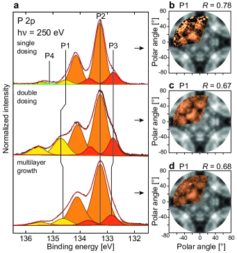
a: XPS spectra of the P 2p core level for ‘single-dosed’, ‘double-dosed’ and ‘multilayer’ samples (top to bottom, respectively). The spectral intensities have been normalized to the P2 peak. b-d: Corresponding measured (orange) and simulated (grey) XPD patterns for the ‘single-dosed’ (b), ‘double-dosed’ (c) and ‘multilayer’ (d) samples with .
Our XPD study of encapsulated -layers can offer two different insights into this matter: () We can simulate possible structures with PP nearest neighbors (specifically dimers and clusters) and see if this leads to an improvement in the agreement with the experimental data, and () we can grow a series of samples in which the dopant density within the Si is varied.
First; the measured XPD of P1 at is overlaid on a simulation of PP dimers within the -layer, as shown in Fig. 1g [42]. Both the large reliability factor and a visual comparison of the two patterns suggest that the measured and simulated XPD are poorly correlated. When measured at lower kinetic energy (), the reliability is even worse [42]. We therefore infer that PP dimerization has not occurred in the -layer. Similarly, no convincing improvement was made using a cluster model [42], and hence we conclude that nothing other than individual P atoms substituting in Si sites is needed to satisfactorily explain the experimental results.
Second; we prepared -layer samples using a range of recipes in order to modify the dopant density. In addition to the sharply confined, ‘double-dosed’, high-density recipe described above, we also prepared a lower P concentration ‘single-dosed’/single-layer sample with electron carrier density [20], and a multilayer sample with 8 cycles of -layer growth and subsequent \ceSi encapsulation (its similar to that of the atomically thin, ‘single-’ and ‘double-dosed’ -layers [33, 50, 20, 21]).
A comparison of the XPS and XPD structure for the three different modes of doping is shown in Fig. 2. The \ceP 2p core level spectra are shown for the three samples (‘single-dosed’, ‘double-dosed’, ‘multilayer’) in Fig. 2a. Correspondingly, the associated XPD image plots are shown in Figs. 2b-d. All three XPD measurements shown have been acquired at and follow the modulations of the P1 component from the buried dopant plane(s).
At first glance, all three XPD patterns share the same main features and symmetry as the bulk-like \ceSi simulation (Fig. 1e). They generally have higher -factors due to the reduced bulk-sensitivity at this kinetic energy (, and for single-, double- and multilayer doping, respectively). Between them, the main difference can be seen from the overall signal strength of each P1 plot, where the ‘single-dosed’ sample has a significantly weaker intensity than the other two. Given its \ceSi overlayer, the fact that P1 shows a clear modulation at all is quite impressive. The ‘double-dosed’ sample has a stronger P1 component than the ‘multilayer’ one, despite there being more \ceP dopants present in the latter. This may be a result of small differences in the overlayer thickness, and the fact that Fig. 2a shows the signal after it is normalized to the surface P2 peak: i.e. the multilayer preparation leads to an increased amount of surface \ceP, which makes the sub-surface \ceP appear relatively smaller after normalization. Nevertheless, the similarities of all three systems with bulk \ceSi measurements indicate that they all exhibit similar substitutional \ceP incorporation, and that no evidence of dimerization or clustering can be observed.
To summarize, we have first of all demonstrated that it is possible to use XPD to study the structure of dopants located beneath the surface of a semiconducting host. Although the dopant layer is described as ‘high density’, it is very narrow and contains a relatively small number of dopants (for example, of an atomic layer). This makes it very challenging to study the structure with other methods. Having demonstrated the applicability of XPD, we reveal that the dopants can be accurately described as P atoms substituted into Si sites within the bulk Si crystal. This is contrary to the previous postulations of PP dimer formation [24, 34]. Furthermore, we have used a range of sample preparation methods to create low-density, high-density, and multilayer dopant planes. We show that, in all cases, the best agreement is found by pure substitution of Si with P. Furthermore, we find no evidence to support the notion that dimerization is encouraged by increasing the dopant density or absolute dopant number.
These findings are especially important for the silicon quantum device community where Si:P -layers are utilized as a platform. Until now the dopant structure has not been resolved, and calculations have shown that dopant ordering (such as dimerization) is an important factor in dictating the valley splitting [23, 24]. We therefore also conclude that XPD is an essential tool for the development and optimization of quantum device architectures based on sub-surface dopant assemblies – such as the much prized -layer platform.
I Methods
I.1 Sample Growth
Surfaces of -type Si(001) with negligible surface oxide on them were prepared in-vacuum by short cycles of high-temperature annealing to (measured with pyrometer, ). The clean surfaces revealed a reconstruction when investigated using low-energy electron diffraction (LEED), as shown in Fig. 3b. Next, the surfaces were exposed to Langmuirs (L) of gaseous \cePH3 (partial pressure mbar for 5 mins) and subsequently annealed to to dissociate the \cePH3 and incorporate \ceP into the Si surface [37, 33]. For the ‘double-dosed’ samples, dosing of \cePH3 and subsequent annealing were repeated twice [34]. For the multilayer samples, 8 cycles of \cePH3 dosing, annealing and subsequent deposition of 1 atomic Si layer were performed [50]. Finally, all dopants were encapsulated by Si and given a short, post-deposition anneal to for a few seconds. This triggered a phase re-ordering of the Si surface (Figs. 3c, 3d).
I.2 Photoemission Measurements
High-resolution X-ray photoelectron spectroscopy (XPS) measurements of the \ceSi 2p and \ceP 2p core levels were performed, throughout the preparation of the ‘single-dosed’, ‘double-dosed’, and ‘multilayer’ samples. For each finished structure, the same core levels were subsequently measured using X-ray photoelectron diffraction (XPD). All photoemission measurements were performed at the SuperESCA endstation of Elettra Synchrotron in Trieste, Italy. All spectra were collected at room temperature (), using a SPECS Phoibos electron energy analyzer equipped with a homemade delay-line detector. The overall energy resolution was for all the measurements. The photoexcitation energies were calibrated from the kinetic energy difference of Si 2p peaks that were collected using first- and second-order light from the monochromator.
I.2.1 XPS Analysis
The characterization of the ‘single-dosed’ -layer system is summarized in Fig. 3. Starting with a clean, (21)-reconstructed Si(001) surface (Fig. 3b) at room temperature, gaseous \cePH3 was adsorbed and partially dissociated [51, 52, 36, 38]. An overall P surface coverage of 0.17 monolayer (ML) was achieved, as estimated from a simple two-layer attenuation model [43].
Upon annealing, three different doublet components became visible from the P 2p core level (Fig. 3a, I). Each doublet can be described by a Voigt line shape with a spin-orbit energy splitting of and an intensity ratio of . According to the re-interpretation by Wilson et al. [49], the main doublet P2 at binding energy should be from surface-incorporated \ceP species. The other two doublets P1 and P3 appear at the relative energies and , respectively. These have been interpreted as different species of surface \ceP with variations in their local atomic environment [42].
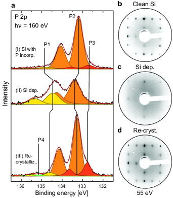
a: The development of the P 2p core level measured at , upon (I) \cePH3 decomposition and dopant incorporation, (II) encapsulation/Si overlayer deposition, and (III) re-crystallization of the Si overlayer. b-d: Surface diffraction (LEED) patterns of the ‘single-dosed’ -layer system (b) before doping, (c) after doping and Si encapsulation, and (d) after re-crystallization of the Si overlayer.
During Si encapsulation (Fig. 3a, II), the surface P2 intensity reduced linearly vs. time, as opposed to the negative exponential decay expected from a simple attenuation model [43]. Additionally, P1 grew in absolute terms. Since a finite amount of P was present in the system, and P2 was assumed to be located at the sample surface at all times (i.e. not attenuated by the addition of Si), the loss of P2 intensity was used to estimate the amount of P1 formed as .
A final anneal to triggered a re-crystallization of the overlayer, as evidenced by the relatively sharp LEED spots and the recurrence of the 21 reconstruction (Figs. 3c, 3d). This final anneal also promoted segregation of \ceP to the surface, and hence the intensity of the surface components (P2 and P3) increased in the XPS (Fig. 3a, II-III). Additionally, a very weak component P4 appeared only in the ‘single-dosed case’, with a disordered spatial structure as determined from its XPD pattern (see the Supplementary note [42]).
By tracing the development the P1 intensity in Fig. 3 (steps I-III) as described, and comparing its final ML coverage to the atomic packing density of the Si(001) plane, the effective electron carrier density was estimated. From ‘single-dosing’ (Fig. 3a), the achieved was estimated to be in the buried -layer. This is well above the metal-to-insulator transition [53], and roughly consistent with previous reports [51, 33, 20].
I.2.2 XPD Analysis
XPD patterns from each finished sample were produced by measuring the \ceSi 2p and \ceP 2p core levels – therein including the sub-components of the buried -layer, over a wide azimuthal sector (), and from grazing () to normal emission (). Each measured spectrum (851 per XPD pattern) was fitted with symmetric Voigt functions to deconvolve the various sub-components present. The intensity of each fitted sub-component was then used to produce polar plots of their modulation functions (commonly referred to as ‘stereographic projections’ [31]), defined as
| (1) |
where is the average intensity for a given across all the azimuthal () scans [32].
I.3 Determining the -Layer Structure
Simulated diffraction patterns from different dopant positions were obtained using the ‘Electron Diffraction in Atomic Clusters’ (EDAC) package [54]. The degree of agreement between each measured and simulated diffraction pattern was quantified by a ‘reliability’ factor :
| (2) |
where and correspond to the experimental and simulated intensity modulation functions, respectively. The sum index runs over all available data points at the different angles measured. The lower the , the better the agreement between the experiment and the atomic model ( corresponds to a complete agreement; means no correlation; signifies anti-correlation [30]). The best understanding of the atomic arrangement was determined by minimizing upon iterative adjustments of the simulated XPD, with subsequent comparison to the experimental XPD, until an optimum fit between the two was reached.
II Data Availability
The data underpinning the findings presented in this publication can be made available from the corresponding author upon reasonable request.
III Acknowledgements
This work was partly supported by the Research Council of Norway (RCN) through project numbers 324183, 315330, and 262633. Additional financial support was received from CALIPSOplus, under Grant Agreement 730872 from the EU Framework Programme for Research and Innovation HORIZON 2020. We acknowledge Elettra Sincrotrone Trieste for providing access to its synchrotron radiation facilities and for all technical assistance. We would also like to thank Ph. Hofmann, J. A. Miwa, M. Bianchi, F. Mazzola, S. P. Cooil, A. J. Holt, and J. Bakkelund for fruitful discussions.
IV Author Contributions
H.I.R., F.S.S., A.C.Å., and J.W.W. measured the XPS and LEED data, which was in turn analyzed by H.I.R. and A.C.Å. The XPD simulations were performed by E.T. with input from all co-authors. H.I.R., F.S.S., A.C.Å., J.W.W. E.T., P.L. and S.L. operated the SuperESCA endstation and performed the XPD measurements. The project was conceived and led by J.W.W. The manuscript was written by H.I.R., F.S.S., A.C.Å., and J.W.W. with contributions from all the authors.
References
- Zwanenburg et al. [2013] F. A. Zwanenburg, A. S. Dzurak, A. Morello, M. Y. Simmons, L. C. L. Hollenberg, G. Klimeck, S. Rogge, S. N. Coppersmith, and M. A. Eriksson, Silicon quantum electronics, Rev. Mod. Phys. 85, 961 (2013).
- Veldhorst et al. [2017] M. Veldhorst, H. G. J. Eenink, C. H. Yang, and A. S. Dzurak, Silicon CMOS architecture for a spin-based quantum computer, Nat. Commun. 8, 1766 (2017).
- Gonzalez-Zalba et al. [2021] M. F. Gonzalez-Zalba, S. de Franceschi, E. Charbon, T. Meunier, M. Vinet, and A. S. Dzurak, Scaling silicon-based quantum computing using CMOS technology, Nat. Electron. 4, 872 (2021).
- Sigillito et al. [2019] A. J. Sigillito, M. J. Gullans, L. F. Edge, M. Borselli, and J. R. Petta, Coherent transfer of quantum information in a silicon double quantum dot using resonant swap gates, npj Quantum Inf. 5, 110 (2019).
- Ciriano-Tejel et al. [2021] V. N. Ciriano-Tejel, M. A. Fogarty, S. Schaal, L. Hutin, B. Bertrand, L. Ibberson, M. F. Gonzalez-Zalba, J. Li, Y.-M. Niquet, M. Vinet, and J. J. Morton, Spin Readout of a CMOS Quantum Dot by Gate Reflectometry and Spin-Dependent Tunneling, PRX Quantum 2, 010353 (2021).
- Pauka et al. [2021] S. J. Pauka, K. Das, R. Kalra, A. Moini, Y. Yang, M. Trainer, A. Bousquet, C. Cantaloube, N. Dick, G. C. Gardner, M. J. Manfra, and D. J. Reilly, A cryogenic CMOS chip for generating control signals for multiple qubits, Nat. Electron. 4, 64 (2021).
- Fuechsle et al. [2012] M. Fuechsle, J. A. Miwa, S. Mahapatra, H. Ryu, S. Lee, O. Warschkow, L. C. Hollenberg, G. Klimeck, and M. Y. Simmons, A single-atom transistor, Nat. Nanotechnol. 7, 242 (2012).
- Veldhorst et al. [2015] M. Veldhorst, C. H. Yang, J. C. C. Hwang, W. Huang, J. P. Dehollain, J. T. Muhonen, S. Simmons, A. Laucht, F. E. Hudson, K. M. Itoh, A. Morrello, and A. S. Dzurak, A two-qubit logic gate in silicon, Nature 526, 410 (2015).
- Schofield et al. [2003] S. R. Schofield, N. J. Curson, M. Y. Simmons, F. J. Rueß, T. Hallam, L. Oberbeck, and R. G. Clark, Atomically Precise Placement of Single Dopants in Si, Phys. Rev. Lett. 91, 136104 (2003).
- Fuechsle et al. [2010] M. Fuechsle, S. Mahapatra, F. A. Zwanenburg, M. Friesen, M. A. Eriksson, and M. Y. Simmons, Spectroscopy of few-electron single-crystal silicon quantum dots, Nat. Nanotechnol. 5, 502 (2010).
- Weber et al. [2012] B. Weber, S. Mahapatra, H. Ryu, S. Lee, A. Fuhrer, T. C. G. Reusch, D. L. Thompson, W. C. T. Lee, G. Klimeck, L. C. L. Hollenberg, and M. Y. Simmons, Ohm’s law survives to the atomic scale, Science 335, 64 (2012).
- Goh et al. [2004] K. E. J. Goh, L. Oberbeck, M. Y. Simmons, A. R. Hamilton, and R. G. Clark, Effect of encapsulation temperature on Si:P delta-doped layers, Appl. Phys. Lett. 85, 4953 (2004).
- Goh and Simmons [2009] K. E. J. Goh and M. Y. Simmons, Impact of Si growth rate on coherent electron transport in Si:P delta-doped devices, Appl. Phys. Lett. 95, 142104 (2009).
- Drumm et al. [2012] D. W. Drumm, L. C. L. Hollenberg, M. Y. Simmons, and M. Friesen, Effective mass theory of monolayer doping in the high-density limit, Phys. Rev. B 85, 155419 (2012).
- McKibbin et al. [2010] S. R. McKibbin, W. R. Clarke, and M. Y. Simmons, Investigating the surface quality and confinement of Si:P -layers at different growth temperatures, Physica E Low Dimens. Syst. Nanostruct. 42, 1180 (2010), 18th International Conference on Electron Properties of Two-Dimensional Systems.
- Polley et al. [2012] C. M. Polley, W. R. Clarke, J. A. Miwa, M. Y. Simmons, and J. W. Wells, Microscopic four-point-probe resistivity measurements of shallow, high density doping layers in silicon, Appl. Phys. Lett. 101, 262105 (2012).
- Miwa et al. [2013] J. A. Miwa, P. Hofmann, M. Y. Simmons, and J. W. Wells, Direct measurement of the band structure of a buried two-dimensional electron gas, Phys. Rev. Lett. 110, 136801 (2013).
- Miwa et al. [2014] J. A. Miwa, O. Warschkow, D. J. Carter, N. A. Marks, F. Mazzola, M. Y. Simmons, and J. W. Wells, Valley splitting in a silicon quantum device platform, Nano Lett. 14, 1515 (2014).
- Mazzola et al. [2014a] F. Mazzola, C. M. Polley, J. A. Miwa, M. Y. Simmons, and J. W. Wells, Disentangling phonon and impurity interactions in -doped Si(001), Appl. Phys. Lett. 104, 173108 (2014a).
- Holt et al. [2020] A. J. Holt, S. K. Mahatha, R.-M. Stan, F. S. Strand, T. Nyborg, D. Curcio, A. K. Schenk, S. P. Cooil, M. Bianchi, J. W. Wells, P. Hofmann, and J. A. Miwa, Observation and origin of the manifold in Si:P layers, Phys. Rev. B 101, 121402 (2020).
- Mazzola et al. [2020] F. Mazzola, C.-Y. Chen, R. Rahman, X.-G. Zhu, C. M. Polley, T. Balasubramanian, P. D. King, P. Hofmann, J. A. Miwa, and J. W. Wells, The sub-band structure of atomically sharp dopant profiles in silicon, npj Quantum Mater. 5, 1 (2020).
- Carter et al. [2009] D. J. Carter, O. Warschkow, N. A. Marks, and D. R. McKenzie, Electronic structure models of phosphorus -doped silicon, Phys. Rev. B 79, 033204 (2009).
- Lee et al. [2011] S. Lee, H. Ryu, H. Campbell, L. C. L. Hollenberg, M. Y. Simmons, and G. Klimeck, Electronic structure of realistically extended atomistically resolved disordered Si:P -doped layers, Phys. Rev. B 84, 205309 (2011).
- Carter et al. [2011] D. J. Carter, N. A. Marks, O. Warschkow, and D. R. McKenzie, Phosphorus -doped silicon: mixed-atom pseudopotentials and dopant disorder effects, Nanotechnology 22, 065701 (2011).
- Chubarov et al. [2018] M. Chubarov, T. H. Choudhury, X. Zhang, and J. M. Redwing, In-plane x-ray diffraction for characterization of monolayer and few-layer transition metal dichalcogenide films, Nanotechnology 29, 055706 (2018).
- Yamashita et al. [2018] S. Yamashita, J. Kikkawa, K. Yanagisawa, T. Nagai, K. Ishizuka, and K. Kimoto, Atomic number dependence of Z contrast in scanning transmission electron microscopy, Sci. Rep. 8, 1 (2018).
- Young et al. [2022] S. M. Young, A. M. Katzenmeyer, E. M. Anderson, T. S. Luk, J. A. Ivie, S. W. Schmucker, X. Gao, and S. Misra, Suppression of mid-infrared plasma resonance due to quantum confinement in delta-doped silicon (2022).
- Hüfner [2013] S. Hüfner, Photoelectron spectroscopy: principles and applications (Springer Science & Business Media, Berlin, 2013) Chap. 11.
- Bengió et al. [2007] S. Bengió, J. Wells, T. Kim, G. Zampieri, L. Petaccia, S. Lizzit, and P. Hofmann, The structure of Sb(111) determined by photoelectron diffraction, Surf. Sci. 601, 2908 (2007).
- Woodruff [2007] D. Woodruff, Adsorbate structure determination using photoelectron diffraction: Methods and applications, Surf. Sci. Rep. 62, 1 (2007).
- Bignardi et al. [2019] L. Bignardi, D. Lizzit, H. Bana, E. Travaglia, P. Lacovig, C. E. Sanders, M. Dendzik, M. Michiardi, M. Bianchi, M. Ewert, L. Buß, J. Falta, J. I. Flege, A. Baraldi, R. Larciprete, P. Hofmann, and S. Lizzit, Growth and structure of singly oriented single-layer tungsten disulfide on Au(111), Phys. Rev. Mater. 3, 014003 (2019).
- Holt et al. [2021] A. J. U. Holt, S. Pakdel, J. Rodríguez-Fernández, Y. Zhang, D. Curcio, Z. Sun, P. Lacovig, Y.-X. Yao, J. V. Lauritsen, S. Lizzit, N. Lanatà, P. Hofmann, M. Bianchi, and C. E. Sanders, Electronic properties of single-layer CoO2/Au(111), 2D Mater. 8, 035050 (2021).
- McKibbin et al. [2009] S. McKibbin, W. Clarke, A. Fuhrer, T. Reusch, and M. Simmons, Investigating the regrowth surface of Si:P -layers toward vertically stacked three dimensional devices, Appl. Phys. Lett. 95, 233111 (2009).
- McKibbin et al. [2014] S. McKibbin, C. Polley, G. Scappucci, J. Keizer, and M. Simmons, Low resistivity, super-saturation phosphorus-in-silicon monolayer doping, Appl. Phys. Lett. 104, 123502 (2014).
- Wang et al. [1994] Y. Wang, M. J. Bronikowski, and R. J. Hamers, An atomically resolved STM study of the interaction of phosphine with the silicon (001) surface, J. Phys. Chem. 98, 5966 (1994).
- Wilson et al. [2004] H. F. Wilson, O. Warschkow, N. A. Marks, S. R. Schofield, N. J. Curson, P. V. Smith, M. W. Radny, D. R. McKenzie, and M. Y. Simmons, Phosphine Dissociation on the Si(001) Surface, Phys. Rev. Lett. 93, 226102 (2004).
- Curson et al. [2004] N. J. Curson, S. R. Schofield, M. Y. Simmons, L. Oberbeck, J. L. O’Brien, and R. G. Clark, STM characterization of the Si-P heterodimer, Phys. Rev. B 69, 195303 (2004).
- Warschkow et al. [2005] O. Warschkow, H. F. Wilson, N. A. Marks, S. R. Schofield, N. J. Curson, P. V. Smith, M. W. Radny, D. R. McKenzie, and M. Y. Simmons, Phosphine adsorption and dissociation on the Si(001) surface: An ab initio survey of structures, Phys. Rev. B 72, 125328 (2005).
- Song et al. [2012] F. Song, Å. Monsen, Z. Li, E.-M. Choi, J. MacManus-Driscoll, J. Xiong, Q. Jia, E. Wahlström, and J. Wells, Extracting the near surface stoichiometry of thin films; a finite element maximum entropy approach, Surf. Sci. 606, 1771 (2012).
- Mazzola et al. [2014b] F. Mazzola, M. T. Edmonds, K. Høydalsvik, D. J. Carter, N. A. Marks, B. C. Cowie, L. Thomsen, J. Miwa, M. Y. Simmons, and J. W. Wells, Determining the electronic confinement of a subsurface metallic state, ACS Nano 8, 10223 (2014b).
- Cooil et al. [2017] S. P. Cooil, F. Mazzola, H. W. Klemm, G. Peschel, Y. R. Niu, A. A. Zakharov, M. Y. Simmons, T. Schmidt, D. A. Evans, J. A. Miwa, and J. W. Wells, In situ patterning of ultrasharp dopant profiles in silicon, ACS Nano 11, 1683 (2017).
- [42] See Supplementary Information for details of sample preparation, XPS depth-dependent analysis, and additional XPD data and modelling.
- Røst et al. [2021] H. I. Røst, R. K. Chellappan, F. S. Strand, A. Grubišić-Čabo, B. P. Reed, M. J. Prieto, L. C. Tǎnase, L. de Souza Caldas, T. Wongpinij, C. Euaruksakul, T. Schmidt, A. Tadich, B. C. C. Cowie, Z. Li, S. P. Cooil, and J. W. Wells, Low-Temperature Growth of Graphene on a Semiconductor, J. Phys. Chem. C 125, 4243 (2021).
- Kittel and McEuen [2018] C. Kittel and P. McEuen, Introduction to Solid State Physics, 8th ed. (John Wiley & Sons, 2018) Chap. 1.
- Bana et al. [2018] H. Bana, E. Travaglia, L. Bignardi, P. Lacovig, C. E. Sanders, M. Dendzik, M. Michiardi, M. Bianchi, D. Lizzit, F. Presel, D. De Angelis, N. Apostol, P. K. Das, J. Fujii, I. Vobornik, R. Larciprete, A. Baraldi, P. Hofmann, and S. Lizzit, Epitaxial growth of single-orientation high-quality MoS2 monolayers, 2D Mater. 5, 035012 (2018).
- Ramstad et al. [1995] A. Ramstad, G. Brocks, and P. J. Kelly, Theoretical study of the Si(100) surface reconstruction, Phys. Rev. B 51, 14504 (1995).
- Tang et al. [1992] S. Tang, A. J. Freeman, and B. Delley, Structure of the Si(100) surface: Total-energy and force analysis of the dimer models, Phys. Rev. B 45, 1776 (1992).
- Tsukidate and Suemitsu [1999] Y. Tsukidate and M. Suemitsu, Saturated adsorption of PH3 on Si(100):P and its application to digital control of phosphorus coverage on Si(100) surface, Appl. Surf. Sci. 151, 148 (1999).
- Wilson et al. [2006] H. F. Wilson, O. Warschkow, N. A. Marks, N. J. Curson, S. R. Schofield, T. C. G. Reusch, M. W. Radny, P. V. Smith, D. R. McKenzie, and M. Y. Simmons, Thermal dissociation and desorption of on Si(001): A reinterpretation of spectroscopic data, Phys. Rev. B 74, 195310 (2006).
- Keizer et al. [2015] J. G. Keizer, S. R. McKibbin, and M. Y. Simmons, The Impact of Dopant Segregation on the Maximum Carrier Density in Si:P Multilayers, ACS Nano 9, 7080 (2015).
- Lin et al. [1999] D.-S. Lin, T.-S. Ku, and T.-J. Sheu, Thermal reactions of phosphine with Si(100): A combined photoemission and scanning-tunneling-microscopy study, Surf. Sci. 424, 7 (1999).
- Lin et al. [2000] D.-S. Lin, T.-S. Ku, and R.-P. Chen, Interaction of phosphine with Si(100) from core-level photoemission and real-time scanning tunneling microscopy, Phys. Rev. B 61, 2799 (2000).
- Kravchenko and Sarachik [2003] S. Kravchenko and M. P. Sarachik, Metal–insulator transition in two-dimensional electron systems, Rep. Prog. Phys. 67, 1 (2003).
- García de Abajo et al. [2001] F. J. García de Abajo, M. A. Van Hove, and C. S. Fadley, Multiple scattering of electrons in solids and molecules: A cluster-model approach, Phys. Rev. B 63, 075404 (2001).