suppl
Antiferromagnetic metal phase in an electron-doped rare-earth nickelate
Long viewed as passive elements, antiferromagnetic materials have emerged as promising candidates for spintronic devices due to their insensitivity to external fields and potential for high-speed switching. Recent work exploiting spin and orbital effects has identified ways to electrically control and probe the spins in metallic antiferromagnets, especially in noncollinear or noncentrosymmetric spin structures. The rare earth nickelate NdNiO3 is known to be a noncollinear antiferromagnet where the onset of antiferromagnetic ordering is concomitant with a transition to an insulating state. Here, we find that for low electron doping, the magnetic order on the nickel site is preserved while electronically a new metallic phase is induced. We show that this metallic phase has a Fermi surface that is mostly gapped by an electronic reconstruction driven by the bond disproportionation. Furthermore, we demonstrate the ability to write to and read from the spin structure via a large zero-field planar Hall effect. Our results expand the already rich phase diagram of the rare-earth nickelates and may enable spintronics applications in this family of correlated oxides.
In recent years, antiferromagnetic materials have become leading contenders for spintronic devices. In comparison with their ferromagnetic counterparts, more subtle methods to control the ordered spins (writing) and to probe such control (reading) are required Baltz2018 . The most widely used method in antiferromagnets is the same as that in ferromagnets – measuring a component of the anisotropic magnetoresistance (AMR) signalMcGuire1975 ; Daughton1992 . This signal strength is typically limited to just a couple percent of the sample’s resistance, however, which limits high-density applicationsJungwirth2016 . This has driven parallel attempts to discover additional read-out methods as well as to identify metallic antiferromagnets with larger AMR signalsSurgers2017 ; Arpaci2021 .
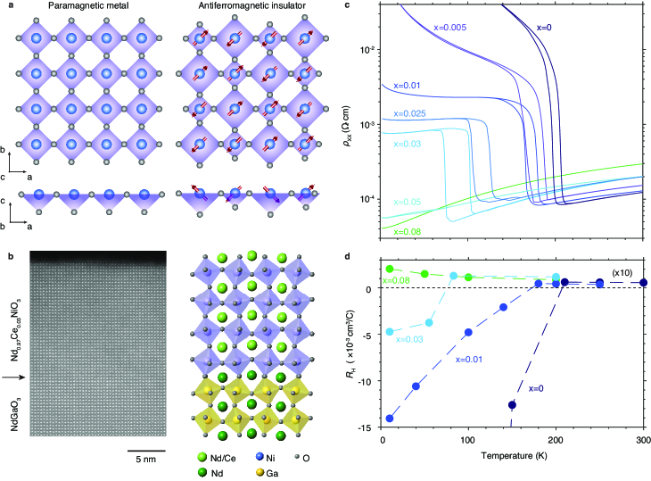
Here we develop a metallic antiferromagnet and demonstrate nearly an order of magnitude stronger AMR signal over conventional antiferromagnets. We begin with the rare-earth nickelates (NiO3), transition metal oxides which sit at the boundary between localized and itinerant electron behaviors. With the exception of LaNiO3, an unconventional metalzhou2014mass with the largest rare-earth cation , the NiO3 compounds undergo a metal-insulator transition (MIT) and a transition from a paramagnetic to a noncollinear antiferromagnetic stateTorrance1992 ; Scagnoli2006 ; Bodenthin2011 . In PrNiO3 and NdNiO3 bulk crystals, the onsets of the antiferromagnetic and insulating states are coincident ()Medarde1997 ; Bodenthin2011 ; Catalano2018 ; Middey2016 . In addition, at the MIT a breathing-mode distortion occurs where half of NiO6 octahedra are expanded and half are compressed in an alternating pattern: a charge order sets in without any 3/3 charge fluctuation on the nickel sites, known as “bond disproportionation”Johnston2014 ; Green2016 ; Varignon2017 ; chargeorder (shown schematically in Fig. 1a).
While the rare earth nickelates thus display coupled spin, charge and lattice degrees of freedom, as well as robust metallic and antiferromagnetic states, to date an antiferromagnetic metal phase has not yet been identifiedWang2018 . We choose NdNiO3, which displays a direct transition from a paramagnetic metal to a noncollinear antiferromagnetic insulator at the highest temperature within the NiO3 series Lacorre1991 ; GarciaMunoz1992 ; Frano2013 . Previous studies have found that strong compressive strainLiu2010 ; Mikheev2015 ; Hauser2015 or hole doping on the neodymium siteCheong1994 ; Alonso1995 ; GarciaMunoz1995 tends to suppress the MIT and leaves a paramagnetic metal state, reminiscent of that found in LaNiO3. In contrast, electron doping of bulk crystals through Th4+ (ref. Alonso1995, ) or Ce4+ (ref. Cheong1994, ; GarciaMunoz1995, ) substitution in the place of Nd3+ has been reported to result only in a modest suppression in the MIT transition temperature. Other studies have found electron-doping through oxygen vacancies stabilizes a persistent antiferromagnetic state yet this state is even more resistive than the parent NdNiO3 phaseLi2021 ; Heo2017 .
Here, we employ electron doping of epitaxial NdNiO3 thin films through substitution of Ce4+ on the Nd3+ lattice site. We find that cerium substitution rapidly induces a metal-metal transition (MMT) where the low-temperature metallic phase retains the antiferromagnetism on the nickel sites of the parent NdNiO3. In contrast to the metallic phase above MMT and MIT, the Fermi surface below the MMT is largely gapped with spectral weight confined to discrete high-intensity spots. Moreover, in this low-temperature phase we demonstrate heat-assisted magnetic recording with a maximum measured amplitude of 18%, bringing a family of materials into the spintronics community and suggesting a pathway to stronger AMR readout signals in antiferromagnets.
Epitaxial films of CexNd1-xNiO3 were synthesized by reactive oxide molecular-beam epitaxy (MBE) on (100)pc NdGaO3 ((110) in orthorhombic notation for the Pnma space group), which provides 1% tensile strain (see Methods). All crystallographic directions referenced throughout this work follow the pseudocubic (pc) notation. Fig. 1b shows the high-angle annular dark field scanning transmission electron microscopy (HAADF-STEM) image of the Ce0.03Nd0.97NiO3 compound. Additional HAADF-STEM and electron energy loss spectroscopy (EELS) maps found in the supplement support the high structural quality and absence of cerium phase segregation or local lattice deformations in these samples (Supplementary Fig. S1, Fig. S5). X-ray absorption spectroscopy data on the Ce-, Nd- and O- pre-peak edges confirm the prototypical Ce4+ and Nd3+ valence states, and indicate electron doping onto the nickel sites (Supplementary Fig. S6).
As seen in Fig. 1c, cerium substitution results in qualitative changes in the transport properties of the films. The parent compound NdNiO3 shows a MIT at 200 K with a resistivity increase of about five orders of magnitude Granados1993 . For intermediate cerium doping (0.01 0.06) the resistivity increases when cooling through the MMT but recovers a behavior, indicative of a metallic phase and a MMT as opposed to the MIT of the parent compound. These samples also demonstrate slight resistive upturns at sufficiently low temperature (below about 10 K), but we believe this to be due to weak localization effects, as suggested by the negative magnetoresistance shown in Supplementary Fig. S21. For higher doping ( 0.06), the transition is fully suppressed and the films remain metallic at all temperatures. We note the emergence of this MMT transition and fully metallic samples was not observed in previous cerium-doped NdNiO3 powder samplesCheong1994 ; GarciaMunoz1995 . Our DFT calculations shown in Supplementary Fig. S13independently demonstrate this behavior as well. In NdNiO3, the sign of the Hall coefficient (Fig. 1d) changes from positive to negative as the system is cooled below Hauser2013 ; Hauser2015 . The same sign change is observed for 0.01 0.06 at , indicating a change in the dominant charge carries from holes to electrons still occurs across the MMT.
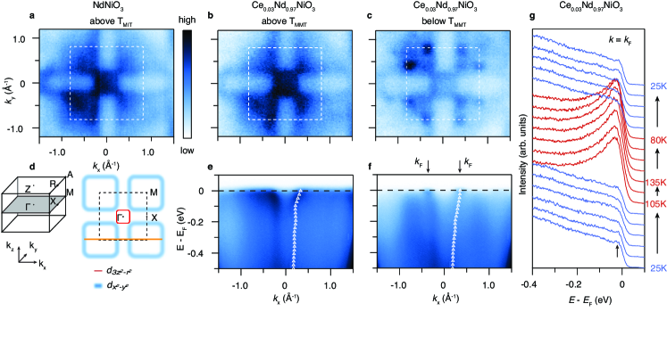
We use angle-resolved photoemission spectroscopy (ARPES) to show that the MMT results in a distinct fermiology at low temperature. Figure 2a-c show ARPES data measured on the XM high-symmetry plane of the three-dimensional Brillouin zone sketched in Fig. 2d. The Fermi surface of NdNiO3 above consists of a small electron pocket centered at (predominantly of orbital character) and a larger hole pocket centered at (predominately of character), visible due to the broadening intrinsic to the measurement. This band structure is consistent with prior measurements of NdNiO3 above Dhaka2015 and is equivalent to that of the fully metallic LaNiO3Yoo2015 ; King2014 . As shown in Fig. 2b there are no perceptible differences between the Fermi surfaces of Ce0.03Nd0.97NiO3 and NdNiO3 at 200 K, within the experimental resolution and data quality. In contrast, below the Fermi surface of Ce0.03Nd0.97NiO3 does not vanish (Fig. 2c) as it does for insulating NdNiO3Dhaka2015 (see Supplementary Fig. S7), but instead turns into a distinctive pattern of discontinuous high-intensity spots located roughly along the original hole pocket contour measured above the transition. This strong reduction of spectral weight of the hole-like Fermi surface is consistent with the change of sign, from positive to negative, observed in at in Fig. 1d. For the fully metallic Ce0.1Nd0.9NiO3, the band structure instead does not show any temperature variation or any noticeable difference with respect to the metallic phase of NdNiO3 (Supplementary Fig. S11). The existence of a unique low temperature Fermi surface in the Ce-doped samples hosting a metal-metal transition helps to dismiss concerns of phase coexistence as has been seen in prior nickelate research Granados1993 ; Obradors1993 .
In Fig. 2e,f we compare the dispersion above and below for Ce0.03Nd0.97NiO3 along the MXM line that cuts through one of the high-intensity spots. At high temperature, the band shows a metallic Fermi edge over a broad momentum range, consistent with the XM plane being close to the boundary of the hole pocket in the direction. At low temperature, the spectral weight at the Fermi level () is suppressed for most of the range, but at some values the metallic edge persists (a more detailed analysis is shown in Supplementary Fig. S8, Fig. S10). Varying the temperature within either metallic phase does not result in any appreciable modification to the maps of Fig. 2e,f, while the change is instead abrupt at the transition. Fig. 2g shows the evolution of the energy dispersion curves (EDCs) taken at the Fermi vector () determined in Fig. 2f, as the temperature is cycled through the MMT . During the warm-up the intensity at suddenly converts into a broad peak at 105 K that remains unchanged until cooling down to 80 K, in a hysteresis cycle which perfectly matches that observed in the resistivity curves of Fig. 1c. Notice that the EDCs of these hot spots retain a metallic edge over the whole temperature range. At the lowest temperature (25 K) there is a distinguishable peak-dip lineshape with a small quasiparticle, as opposed to the rest of the Fermi surface which is gapped or pseudogapped below (see also the analysis in Fig. S7, S8, S9). Thus both our electrical transport and ARPES measurements independently show the new metallic phase below MMT in our intermediate cerium doped samples.
The Fermi surface of Fig. 2c clearly shows the presence of a new, smaller periodicity in momentum space. Even though it is difficult to sketch the band backfolding due to the presence of multiple bands and of the spectral weight added by the broadening, the pattern formed by the high intensity spots is consistent with a superstructure, where the and A points are brought into each other, as well as Z and M (Supplementary Fig. S11). On the ZRA plane weak signatures of this superstructure are present in (metallic) LaNiO3 Yoo2015 , as well as here in CexNd1-xNiO3 for all doping levels above the MIT/MMT (Supplementary Fig. S11), which may originate from dynamic charge-order fluctuations as discussed in Supplementary material. Piamonteze2005 ; Green2016 .
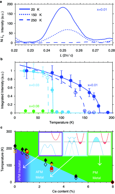
To probe the antiferromagnetic order in this low-temperature metallic phase, we use neutron diffraction and site-specific resonant x-ray scattering (RXS). Neutron diffraction (Supplementary Fig. S15) shows that the parent NdNiO3 is antiferromagnetically ordered as reported in the literatureScagnoli2006 ; Scagnoli2008 . Figure 3a shows RXS data from the Ni- edge of Ce0.01Nd0.99NiO3, measured along () with fixed (, ) = (, ). We observe an onset of antiferromagnetic order below . The temperature dependence of the (normalized) integrated signal is shown in Fig. 3b for , and . The absolute integrated signal intensity decreases from the x=0.01 to the x=0.03 sample; see Supplemental figure S15 and the accompanying discussion for more details. As an additional verification of antiferromagnetic order in the x=0.03 sample, we performed optical second-harmonic generation measurements, which concur with the findings from the RXS measurements presented here (see Supplemental Fig. S18). In contrast to NdNiO3, the magnetic order on the neodymium sites is not present below . This is apparent both in the Nd- resonant x-ray scattering as well as the absence of observed order in the neutron scattering which is primarily sensitive to the neodymium order (Supplementary Fig. S15. Finally, the metallic Ce0.08Nd0.92NiO3 film lacks observable magnetic ordering on either cation site. Note that we are unable to distinguish a collinear versus noncollinear microscopic ordering from the presented data, however based off of prior works the noncollinear order is the most likely origin of the measured periodicity in our samplesHepting2018 ; Scagnoli2006 .
The CexNd1-xNiO3 system thus shows three distinct regions as shown in Fig. 3c. For , there is a transition from a paramagnetic metal to an insulator with antiferromagnetic order on both the neodymium and nickel sites. For , the MIT is replaced by a MMT with antiferromagnetic order remaining on the nickel sites in the low-temperature metallic phase. For , the material lacks evidence of magnetic order, and is likely a paramagnetic metal at all temperatures, similar to LaNiO3Sreedhar1992 or NdNiO3 under compressive strain Liu2010 ; Mikheev2015 ; Hauser2015 .
While the insulating phase in the NiO3 family is believed to result from a combination of the lattice distortion and of electronic correlations Mazin2007 ; Johnston2014 ; Green2016 ; Georgescu2019 , the MMT offers the possibility to partially decouple the two contributions to the transition: Peierls-type and Mott-typeRuppen2015 . From our data in Fig. 2b,c, we argue that in this low-temperature metallic phase the Peierls component of the MIT has taken place, but the additional electrons provided by the Ce4+ atoms likely screen correlations just enough that the electron and hole bands are not pushed apart. In this respect, note also that no sizeable bandwidth reduction can be seen in Fig. 2e,f, where both above and below the hole-like band disperses all the way to the onset of the manifold. In this scenario, the charge order is a necessaryZhang2016b but not sufficient condition to induce an insulating phase in the NiO3 family. With suppressed or reduced electronic correlations the system remains metallic while retaining the characteristic noncollinear antiferromagnetic order.
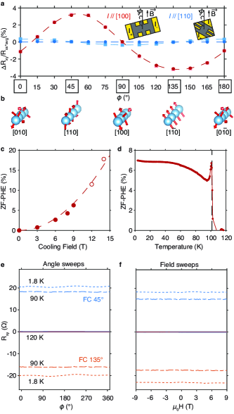
Finally, we demonstrate the manipulation of the antiferromagnetic order in this newly stabilized antiferromagnetic metal phase with an external magnetic field, and probe the spin structure via electrical transport. We measure the zero-field planar Hall effect (ZF-PHE) of Ce0.03Nd0.97NiO3 samples below . Antiferromagnetic materials are expected to display an AMR signal in the presence of a magnetic field as the signal is even (not odd) with the local magnetic moments. Zero-field effects, however, are far less common in antiferromagnets and imply a change to the microscopic spin structureMarti2014 ; Kriegner2016 ; Nair2020 , typically preferential domain formation or canted moment orientation. Figure 4a shows the magnitude of the change in Rxy (normalized by the average Rxx value) versus in-plane angle for current () applied in two directions: parallel to [100] and parallel to [110]. When current is applied along [100], a significant PHE is present. Removing the external magnetic field has minimal effect on the Rxy value, as the ZF-PHE (dark data points) is of the same magnitude as the 9 T PHE (light data points). There is therefore a memory effect written by a cooling field and read by the transverse resistance via the ZF-PHE. Conversely, for current parallel to [110], the 9 T PHE amplitude is reduced by almost an order of magnitude and with the removal of the field, entirely absent (see Methods and Supplementary Figure S19). Figure 4b shows the spin structure of the parent compound NdNiO3 schematically (as found in previous works Frano2013 ; Hepting2018 ) below the corresponding measurement angles in Fig. 4a. There is noncollinearity along [100] and [010], whereas along [110] and , the spins are collinear.
The amplitude of the ZF-PHE for a given cooling field is defined as the overall difference between the peak (at in Fig. 4a) and the trough (in Fig. 4a at ). We find a maximum amplitude of about 18%, which is roughly three times stronger than typically reported ZF-PHE magnitudes in antiferromagnets Jungwirth2016 and, to the best of our knowledge, about equal to the maximum ever reported Nair2020 (see Supplementary Fig. S19). The dependence on , Fig. 4c, roughly follows a simple quadratic up to our maximum used cooling field of 14 T, implying that with stronger fields even larger amplitudes are attainable. The temperature dependence, Fig. 4d, shows a gradual weakening of the effect as the system approaches its transition and a sudden suppression above the MMT (consistent with the Néel transition). Figure 4e,f show constant temperature angle and field sweeps taken after field-cooling the sample at 45o (135o) into its “high” (“low”) Rxy state. The field-cooled states are extremely rigid to external perturbations once they are set; field sweeps over 9 T and rotations in 9 T have negligible impact on the Rxy channel. This is true both at the lowest base temperature of 1.8 K, and at temperatures near but below the transition (90 K shown in the figure).
In ferromagnets, there exist multiple contributions to the AMR signal arising from spin-dependent scattering between conduction electrons and localized magnetic moments Kokado2012 . The degree of polarization of the conduction electrons critically affects the amplitude of the AMR. In collinear antiferromagnets, the current is strictly not spin polarized. But in noncollinear antiferromagnets, spin-polarized currents are generally allowedZelezny2017-noncollinear and thus the nature of how spin-dependent scattering events contribute to the AMR signal is changed. Given our current direction dependence, it is likely the case that a spin polarized current in a noncollinear antiferromagnet either strengthens or allows additional scattering terms which in turn strengthen the ZF-PHE. Follow-up measurements in other noncollinear antiferromagnets would help clarify whether a large amplitude ZF-PHE is a general trend in such systems. Another natural follow-up experiment would be to attempt to electrically switch these devices using current pulses Wadley2016 .
Here we explored electron doping of a prototypical transition metal oxide, NdNiO3. The parent NdNiO3 phase is characterized by both spin and charge ordering, perched at the boundary between localized and itinerant electron behaviors: a transition to an insulating, antiferromagnetic state happens in tandem with bond disproportionation. We showed that electron doping can uncover a metallic phase that preserves antiferromagnetic order on the nickel sites and is triggered by a Fermi surface reconstruction induced by charge ordering. We interpret the new phase synthesized as one giving the opportunity of partially decoupling the lattice and electronic contributions to the famous metal-insulator transition characteristic of the perovskite nickelates. We also find that the electron-doped samples display a large zero-field planar Hall effect, and thus offer a new (possibly noncollinear) antiferromagnetic metal of relevance to the spintronics community.
Acknowledgements
This work is supported by the STC Center for Integrated Quantum Materials, NSF Grant No. DMR-1231319. Materials growth was supported by the National Science Foundation (Platform for the Accelerated Realization, Analysis, and Discovery of Interface Materials (PARADIM)) under Cooperative Agreement No. DMR-2039380. This work used resources of the Advanced Light Source, which is a DOE Office of Science User Facility under contract no. DE-AC02-05CH11231. The ARPES work was partially funded by the U.S. Department of Energy, Office of Science, Office of Basic Energy Sciences, Materials Sciences and Engineering Division under Contract No. DE-AC02-05-CH11231 (Ultrafast Materials Program KC2203). Electron microscopy was carried out through the use of MIT nano facilities at the Massachusetts Institute of Technology. Additional electron microscopy work was performed at Harvard University’s Center for Nanoscale Systems, a member of the National Nanotechnology Coordinated Infrastructure Network, supported by the NSF under Grant No. 2025158. A portion of this research used resources at the Spallation Neutron Source (SNS), a DOE Office of Science User Facility operated by the Oak Ridge National Laboratory (ORNL), and resources of the SNS Second Target Station Project. ORNL is managed by UT-Battelle LLC for DOE’s Office of Science, the single largest supporter of basic research in the physical sciences in the United States. This manuscript has been authored by UT-Battelle, LLC, under contract DE-AC05-00OR22725 with the US Department of Energy (DOE). The US government retains and the publisher, by accepting the article for publication, acknowledges that the US government retains a nonexclusive, paid-up, irrevocable, worldwide license to publish or reproduce the published form of this manuscript, or allow others to do so, for US government purposes. DOE will provide public access to these results of federally sponsored research in accordance with the DOE Public Access Plan (http://energy.gov/downloads/doe-public-access-plan). Device fabrication work was performed at Harvard University’s Center for Nanoscale Systems (CNS), a member of the National Nanotechnology Coordinated Infrastructure Network (NNCI), supported by the National Science Foundation under NSF Grant No. 1541959. Any mention of commercial products within this paper is for information only; it does not imply recommendation or endorsement by NIST. Work at the NCNR was supported by the Department of Commerce. W. R. acknowledges support from the Department of Commerce. S.D. acknowledges support from the NSF Graduate Research Fellowship Grant No. DGE-1745303. G.A.P. acknowledges support from the Paul & Daisy Soros Fellowship for New Americans and from the NSF Graduate Research Fellowship Grant No. DGE-1745303. H.E. and I.E. were supported by The Rowland Institute at Harvard. J.N. acknowledges support from the Swiss National Science Foundation under Project No. P2EZP2_195686. C.T. acknowledges support from the Swiss National Science Foundation under Project No. P2EZP2_191801. Work in the S.-Y.X. group was supported through NSF Career (Harvard fund 129522) DMR-2143177. H.L. and A.S.B. acknowledges support from NSF Grant No. DMR-2045826 and the ASU Research Computing Center for HPC resources. J.A.M acknowledges support from the Packard Foundation and Gordon and Betty Moore Foundation’s EPiQS Initiative, Grant GBMF6760.
Author Contributions
Q.S., G.A.P., C.M.B. and J.A.M. synthesized the thin-films with assistance from H.P. Q.S. and L.M. performed the ARPES measurements with support from A.B., C.J., E.R., D.F.S., Z.H., and A.L. S.D., Q.S. and J.A.M. performed the electrical measurements with assistance from J.T.H. H.E. I.E. characterized the samples with scanning transmission electron microscopy. G.A.P., S.D., J.R.E., D.F.S., Q.S., D.C.C., A.T.N. and P.S. performed x-ray spectroscopy and scattering measurements. C.A.H., Y.L. and W.D.R. performed the neutron diffraction measurements. J.N., C.T. and S.-Y.X. performed the SHG measurements. B.P. and A.S.B. performed the DFT calculations. J.A.M. conceived and guided the study. Q.S., S.D., L.M. and J.A.M. wrote the manuscript with discussion and contributions from all authors.
Competing Interests
The authors declare no competing interests.
References
- (1) Baltz, V., Manchon, A., Tsoi, M., Moriyama, T., Ono, T. & Tserkovnyak, Y. Antiferromagnetic spintronics. Rev. Mod. Phys. 90, 015005 (2018).
- (2) McGuire, T. & Potter, R. Anisotropic magnetoresistance in ferromagnetic 3d alloys. IEEE Trans. Magn. 11, 1018-1038 (1975).
- (3) Daughton, J. Magnetoresistive memory technology. Thin Solid Films. 216, 162-168 (1992).
- (4) Jungwirth, T., Marti, X., Wadley, P. & Wunderlich, J. Antiferromagnetic spintronics. Nat. Nanotechnol. 11, 231-241 (2016).
- (5) Sürgers, C., Wolf, T., Adelmann, P., Kittler, W., Fischer, G. & Löhneysen, H. Switching of a large anomalous Hall effect between metamagnetic phases of a non-collinear antiferromagnet. Sci. Rep. 7, 42982 (2017).
- (6) Arpaci, S., Lopez-Dominguez, V., Shi, J., Sánchez-Tejerina, L., Garesci, F., Wang, C., Yan, X., Sangwan, V., Grayson, M., Hersam, M., Finocchio, G. & Amiri, P. Observation of current-induced switching in non-collinear antiferromagnetic IrMn3 by differential voltage measurements. Nat. Commun. 12, 3828 (2021).
- (7) Zhou, J., Marshall, L. & Goodenough, J. Mass enhancement versus Stoner enhancement in strongly correlated metallic perovskites: LaNiO3 and LaCuO3. Phys. Rev. B 89, 245138 (2014).
- (8) Scagnoli, V., Staub, U., Mulders, A., Janousch, M., Meijer, G., Hammerl, G., Tonnerre, J. & Stojic, N. Role of magnetic and orbital ordering at the metal-insulator transition in NdNiO3. Phys. Rev. B 73, 100409 (2006).
- (9) Torrance, J., Lacorre, P., Nazzal, A., Ansaldo, E. & Niedermayer, C. Systematic study of insulator-metal transitions in perovskites RNiO3 (R=Pr, Nd, Sm, Eu) due to closing of charge-transfer gap. Phys. Rev. B 45, 8209-8212 (1992).
- (10) Bodenthin, Y., Staub, U., Piamonteze, C., García-Fernández, M., Martínez-Lope, M. & Alonso, J. Magnetic and electronic properties of RNiO3 (R = Pr, Nd, Eu, Ho and Y) perovskites studied by resonant soft x-ray magnetic powder diffraction. J. Condens. Matter Phys. 23, 036002 (2011).
- (11) Medarde, M. Structural, magnetic and electronic properties of RNiO3 perovskites (R = rare earth). J. Phys. Conden. Matter. 9, 1679-1707 (1997).
- (12) Catalano, S., Gibert, M., Fowlie, J., íñiguez, J., Triscone, J. & Kreisel, J. Rare-earth nickelates RNiO3: thin films and heterostructures. Rep. Prog. Phys. 81, 046501 (2018).
- (13) Middey, S., Chakhalian, J., Mahadevan, P., Freeland, J., Millis, A. & Sarma, D. Physics of Ultrathin Films and Heterostructures of Rare-Earth Nickelates. Annu. Rev. Mater. Res. 46 pp. 305-334 (2016).
- (14) Johnston, S., Mukherjee, A., Elfimov, I., Berciu, M. & Sawatzky, G. Charge disproportionation without charge transfer in the rare-earth-element nickelates as a possible mechanism for the metal-insulator transition. Phys. Rev. Lett. 112, 1-5 (2014).
- (15) Green, R., Haverkort, M. & Sawatzky, G. Bond disproportionation and dynamical charge fluctuations in the perovskite rare-earth nickelates. Phys. Rev. B 94, 195127 (2016).
- (16) Varignon, J., Grisolia, M., íñiguez, J., Barthélémy, A. & Bibes, M. Complete phase diagram of rare-earth nickelates from first-principles. Npj Quantum Mater. 2, 1-8 (2017).
- (17) As common practice in the literature, throughout the paper we will interchangeably refer to this as bond disproportionation/ordering or charge ordering with the understanding that its origin is in the hybridization between the O 2 and the Ni 3 states.
- (18) Wang, B., Rosenkranz, S., Rui, X., Zhang, J., Ye, F., Zheng, H., Klie, R., Mitchell, J. & Phelan, D. Antiferromagnetic defect structure in LaNiO3-δ single crystals. Phys. Rev. Mater. 2, 064404 (2018).
- (19) Lacorre, P., Torrance, J., Pannetier, J., Nazzal, A., Wang, P. & Huang, T. Synthesis, crystal structure, and properties of metallic PrNiO3: Comparison with metallic NdNiO3 and semiconducting SmNiO3. J. Solid State Chem. 91, 225-237 (1991).
- (20) García-Muñoz, J., Rodríguez-Carvajal, J., Lacorre, P. & Torrance, J. Neutron-diffraction study of RNiO3 (R=La, Pr, Nd, Sm): Electronically induced structural changes across the metal-insulator transition. Phys. Rev. B 46, 4414-4425 (1992).
- (21) Frano, A., Schierle, E., Haverkort, M., Lu, Y., Wu, M., Blanco-Canosa, S., Nwankwo, U., Boris, A., Wochner, P., Cristiani, G., Habermeier, H., Logvenov, G., Hinkov, V., Benckiser, E., Weschke, E. & Keimer, B. Orbital Control of Noncollinear Magnetic Order in Nickel Oxide Heterostructures. Phys. Rev. Lett. 111, 106804 (2013).
- (22) Liu, J., Kareev, M., Gray, B., Kim, J., Ryan, P., Dabrowski, B., Freeland, J. & Chakhalian, J. Strain-mediated metal-insulator transition in epitaxial ultrathin films of NdNiO3. Appl. Phys. Lett. 96, 1-4 (2010).
- (23) Mikheev, E., Hauser, A., Himmetoglu, B., Moreno, N., Janotti, A., Van De Walle, C. & Stemmer, S. Tuning bad metal and non-Fermi liquid behavior in a Mott material: Rare-earth nickelate thin films. Sci. Adv. 1, 21-26 (2015).
- (24) Hauser, A., Mikheev, E., Moreno, N., Hwang, J., Zhang, J. & Stemmer, S. Correlation between stoichiometry, strain, and metal-insulator transitions of NdNiO3 films. Appl. Phys. Lett. 106, 092104 (2015).
- (25) Cheong, S., Hwang, H., Batlogg, B., Cooper, A. & Canfield, P. Electron-hole doping of the metal-insulator transition compound ReNiO3. Physica B: Conden. Matter. 194-196 pp. 1087-1088 (1994).
- (26) Alonso, J., Martínez-Lope, M. & Hidalgo, M. Hole and Electron Doping of RNiO3 (R = La, Nd). J. Solid State Chem. 116, 146-156 (1995).
- (27) García-Muñoz, J., Suaaidi, M., Martínez-Lope, M. & Alonso, J. Influence of carrier injection on the metal-insulator transition in electron- and hole-doped R1-xAxNiO3 perovskites. Phys. Rev. B 52, 13563-13569 (1995).
- (28) Li, J., Green, R., Zhang, Z., Sutarto, R., Sadowski, J., Zhu, Z., Zhang, G., Zhou, D., Sun, Y., He, F., Ramanathan, S. & Comin, R. Sudden Collapse of Magnetic Order in Oxygen-Deficient Nickelate Films. Phys. Rev. Lett. 126, 187602 (2021).
- (29) Heo, S., Oh, C., Son, J. & Jang, H. Influence of tensile-strain-induced oxygen deficiency on metal-insulator transitions in NdNiO3-δ epitaxial thin films. Sci. Rep. 7 (2017).
- (30) Granados, X., Fontcuberta, J., Obradors, X., Mañosa, L. & Torrance, J. Metallic state and the metal-insulator transition of NdNiO3. Phys. Rev. B 48, 11666-11672 (1993).
- (31) Hauser, A., Mikheev, E., Moreno, N., Cain, T., Hwang, J., Zhang, J. & Stemmer, S. Temperature-dependence of the Hall coefficient of NdNiO3 thin films. Appl. Phys. Lett. 103, 182105 (2013).
- (32) Dhaka, R., Das, T., Plumb, N., Ristic, Z., Kong, W., Matt, C., Xu, N., Dolui, K., Razzoli, E., Medarde, M., Patthey, L., Shi, M., Radović, M. & Mesot, J. Tuning the metal-insulator transition in NdNiO3 heterostructures via Fermi surface instability and spin fluctuations. Phys. Rev. B 92, 035127 (2015).
- (33) Yoo, H., Hyun, S., Moreschini, L., Kim, H., Chang, Y., Sohn, C., Jeong, D., Sinn, S., Kim, Y., Bostwick, A., Rotenberg, E., Shim, J. & Noh, T. Latent instabilities in metallic LaNiO3 films by strain control of Fermi-surface topology. Sci. Rep. 5, 8746 (2015).
- (34) King, P., Wei, H., Nie, Y., Uchida, M., Adamo, C., Zhu, S., He, X., Božović, I., Schlom, D. & Shen, K. Atomic-scale control of competing electronic phases in ultrathin LaNiO3. Nat. Nanotechnol. 9, 443-447 (2014).
- (35) Obradors, X., Paulius, L., Maple, M., Torrance, J., Nazzal, A., Fontcuberta, J. & Granados, X. Pressure dependence of the metal-insulator transition in the charge-transfer oxides RNiO3 (R=Pr,Nd,Nd0.7La0.3). Phys. Rev. B 47, 12353-12356 (1993).
- (36) Piamonteze, C., Tolentino, H., Ramos, A., Massa, N., Alonso, J., Martínez-Lope, M. & Casais, M. Short-range charge order in RNiO3 perovskites (R=Pr, Nd, Eu, Y) probed by x-ray-absorption spectroscopy. Phys. Rev. B 71, 012104 (2005).
- (37) Scagnoli, V., Staub, U., Bodenthin, Y., García-Fernández, M., Mulders, A., Meijer, G. & Hammerl, G. Induced noncollinear magnetic order of Nd3+ in NdNiO3 observed by resonant soft x-ray diffraction. Phys. Rev. B 77, 14-17 (2008).
- (38) Hepting, M., Green, R., Zhong, Z., Bluschke, M., Suyolcu, Y., Macke, S., Frano, A., Catalano, S., Gibert, M., Sutarto, R., He, F., Cristiani, G., Logvenov, G., Wang, Y., Aken, P., Hansmann, P., Le Tacon, M., Triscone, J., Sawatzky, G., Keimer, B. & Benckiser, E. Complex magnetic order in nickelate slabs. Nat. Phys. 14, 1097-1102 (2018).
- (39) Sreedhar, K., Honig, J., Darwin, M., McElfresh, M., Shand, P., Xu, J., Crooker, B. & Spalek, J. Electronic properties of the metallic perovskite LaNiO3: Correlated behavior of 3d electrons. Phys. Rev. B 46, 6382-6386 (1992).
- (40) Mazin, I., Khomskii, D., Lengsdorf, R., Alonso, J., Marshall, W., Ibberson, R., Podlesnyak, A., Martínez-Lope, M. & Abd-Elmeguid, M. Charge Ordering as Alternative to Jahn-Teller Distortion. Phys. Rev. Lett. 98, 176406 (2007).
- (41) Georgescu, A., Peil, O., Disa, A., Georges, A. & Millis, A. Disentangling lattice and electronic contributions to the metal–insulator transition from bulk vs. layer confined RNiO3. Proc. Natl. Acad. Sci. 116, 14434-14439 (2019).
- (42) Ruppen, J., Teyssier, J., Peil, O., Catalano, S., Gibert, M., Mravlje, J., Triscone, J., Georges, A. & Marel, D. Optical spectroscopy and the nature of the insulating state of rare-earth nickelates. Phys. Rev. B 92, 155145 (2015).
- (43) Zhang, J., Kim, H., Mikheev, E., Hauser, A. & Stemmer, S. Key role of lattice symmetry in the metal-insulator transition of NdNiO3 films. Sci. Rep. 6 (2016).
- (44) Marti, X., Fina, I., Frontera, C., Liu, J., Wadley, P., He, Q., Paull, R., Clarkson, J., Kudrnovský, J., Turek, I., Kuneš, J., Yi, D., Chu, J., Nelson, C., You, L., Arenholz, E., Salahuddin, S., Fontcuberta, J., Jungwirth, T. & Ramesh, R. Room-temperature antiferromagnetic memory resistor. Nat. Mater. 13, 367-374 (2014).
- (45) Kriegner, D., Výborný, K., Olejník, K., Reichlová, H., Novák, V., Marti, X., Gazquez, J., Saidl, V., Němec, P., Volobuev, V., Springholz, G., Holý, V. & Jungwirth, T. Multiple-stable anisotropic magnetoresistance memory in antiferromagnetic MnTe. Nat. Commum. 7, 11623 (2016).
- (46) Nair, N., Maniv, E., John, C., Doyle, S., Orenstein, J. & Analytis, J. Electrical switching in a magnetically intercalated transition metal dichalcogenide. Nat. Mater. 19, 153-157 (2020).
- (47) Kokado , S., Tsunoda , M., Harigaya , K. & Sakuma , A. Anisotropic Magnetoresistance Effects in Fe, Co, Ni, Fe4N, and Half-Metallic Ferromagnet: A Systematic Analysis. J. Phys. Soc. Japan. 81, 024705 (2012).
- (48) Železný, J., Zhang, Y., Felser, C. & Yan, B. Spin-Polarized Current in Noncollinear Antiferromagnets. Phys. Rev. Lett. 119, 187204 (2017).
- (49) Wadley, P., Howells, B., Železný, J., Andrews, C., Hills, V., Campion, R., Novák, V., Olejník, K., Maccherozzi, F., Dhesi, S., Martin, S., Wagner, T., Wunderlich, J., Freimuth, F., Mokrousov, Y., Kuneš, J., Chauhan, J., Grzybowski, M., Rushforth, A., Edmonds, K., Gallagher, B. & Jungwirth, T. Electrical switching of an antiferromagnet. Science 351, 587-90 (2016).
Methods
Growth of Nd1-xCexNiO3 films
CexNd1-xNiO3 thin films were synthesized on (110) NdGaO3 and (100) LaAlO3 substrates by reactive-oxide molecular-beam epitaxy in a Veeco Gen10 system at PARADIM Thin Film growth Facility at Cornell. The substrates were heated to 690°C, determined by a thermocouple next to the substrate heater. A mixture of 80% ozone and 20% oxygen partial pressure of 2 × 10⁻⁶ Torr was used during deposition (1 Torr = 0.133322 kPA). Neodymium, cerium and nickel were evaporated from elemental sources. The fluxes of neodymium and nickel were 1 × 10¹³ atomscm2/sec and the flux of cerium was adjusted according to the desired doping. Following calibration using a quartz crystal microbalance, the three fluxes were first refined by measuring the thickness of Nd2O3 on (111) (ZrO2)0.905(Y2O3)0.09 substrate (denoted as YSZ), CeO2 on (111) YSZ substrate and NiO on (100) MgO substrate, respectively. The neodymium and nickel fluxes were then adjusted to produce a stoichiometric NdNiO3 film as judged by the out-of-plane lattice parameter measured by X-Ray Diffraction (XRD) and the resistivity. The thickness of deposited films varies between 14 nm and 23 nm. The structure was characterized by a PANalytical Empyrean x-ray diffractometer at 45 kV and 40 mA with Cu K radiation.The X-ray diffraction -2 scans indicate that all of the CexNd1-xNiO3 films are single phase grown on NdGaO3 (Fig. S2) and LaAlO3 (Fig. S3) substrates. The comparison of phase diagram of the films grown on NdGaO3 and LaAlO3 is shown in Fig. S4.
Resonant x-ray scattering
Resonant x-ray scattering measurements were performed on Ni- and Nd- edges at Beamline 4.0.2 at the Advanced Light Source at Lawrence Berkeley National Laboratory. Reciprocal space maps (RSMs) were generated by aligning to the signal peak after performing -rod scans, and capturing fixed geometry CCD images for bins around the peak location. Note that the deviation of the peak maximum from the expected is small enough to be due to an alignment offset, and is not directly indicative of any incommensurate order. Reciprocal space maps were measured at a series of temperatures upon warming and cooling each sample and regions of interest were defined around the observed order peaks. To extract integrated intensities, constant size regions of interest were defined around the peak in the RSMs and the total intensity contained was summed. Background intensities (used for background subtraction) were collected in the diffuse regions around the ordering peaks. Small and offsets were added relative to the location of the peak to define a region of background intensity.
X-ray absorption spectroscopy
We use Beamlines 6.3.1 and 4.0.2 at the Advanced Light Source at Lawrence Berkeley National Laboratory to perform x-ray absorption spectroscopy (XAS). Measurements were conducted in the total electron yield geometry. Each spectra shown is the average of 4-16 individual scans. The Nd-M4,5 and Ce-M4,5 spectra were normalized to the pre-edge intensity. The O- edge spectra were normalized to the integrated peak intensity.
Transport measurements
Cr(10 nm)/Au(100 nm) electrical contacts were deposited in the pattern shown by the cartoon of Fig. 4a with an electron-beam evaporator. Channels were etched in with a diamond scribe. A typical device was roughly 3mm x 5mm. Transport measurements were performed in a Quantum Design Dynacool Physical Property Measurement System (PPMS) for fields up to 9 T. In plane rotations were performed using the Quantum Design horizontal rotator option. Measurements performed at 12 T and 14 T were conducted in a 14 T Quantum Design PPMS. Hall coefficients were calculated from linear fits of antisymmetrized field sweeps measured from 9 T; a representative example is shown in Supplemental Figure S22. In Fig. 4e/f, a vertical offset due to contact misalignment was removed.
Angle-resolved photoemission
The ARPES data was measured at the beamline MAESTRO of the Advanced Light Source using a Scienta 4000 electron analyzer. The angular resolution is better than 0.1∘ and the energy resolution varied between 10 meV and 25 meV depending on the setting chosen. The light polarization was set to . In this configuration when the sample is facing the analyzer slit with the axis in the horizontal () direction the electric field is even in the mirror plane plane containing the surface normal and therefore the measurement is sensitive to the and orbitals along , which are both even in the same plane. Prior to the ARPES experiments, the films were annealed in a a partial oxygen pressure of 1 × 10⁻⁵ with 10% ozone at a temperature of 420 °C for approximately one hour.
Neutron Scattering Measurements
Elastic neutron scattering data were collected at the SPINS cold triple-axis spectrometer at the NIST Center for Neutron Research (NCNR) and at the CORELLI elastic diffuse scattering spectrometerye2018implementation at the Oak Ridge National Laboratory Spallation Neutron Source (SNS). The SPINS measurements were taken at a fixed neutron energy of 5 meV with a collimation and filter setup of 80’-Be-80’-Be using a standard closed cycle refrigerator for sample temperature control.
CORELLI is a quasi-Laue time-of-flight instrument with an incident neutron wavelength band between 0.65 and 2.9 Å. The two-dimensional detector array of CORELLI spans from -19∘ to 147∘ in the horizontal plane and from -27∘ to 29∘ vertically. Therefore, a large three-dimensional volumetric reciprocal space is surveyed for a single sample orientation. The sample was mounted to an Al pin at the bottom of a close cycle refrigerator, which provided a base temperature of 3 K at NCNR and 6 K at CORELLI. The sample was mounted with the (h k 0)o plane horizontal, and the vertical rotation axis was along the (0 0 l)o axis. The experiments were conducted by first rotating the film through 120∘ in 1∘ step to survey features in the large reciprocal space, and then data were collected for an extended time with particular sample orientations optimized for the selected reciprocal regions.
Scanning Transmission Electron Microscopy
High-angle annular dark-field STEM measurements were performed either on a JEOL ARM 200F (on the Ce 4% sample) or a Thermo-Fisher Scientific Titan Themis Z G3 (on the Ce 12% sample) both operating at 200 kV. The convergence angle was either 19.6 or 22 mrad and the collection angle range was 68 mrad-280 mrad. Fast-acquisition frames were collected, aligned and summed to minimize drift and obtain high signal-to-noise-ratio. The interfacial strain maps were extracted using the method described in the reference Goodge2022 .
Electron Energy Loss Spectroscopy
Electron energy loss spectroscopy (EELS) were performed on the Thermo-Fisher Scientific Titan Themis Z G3 equipped with a Gatan Continuum spectrometer and imaging filter. The microscope was operated at 200 kV and 100 pA current. Dual (zero-loss and core-loss) EELS spectrum images were acquired simultaneously to correct for energy drift. After determining a region of interest in a zone axis, the electron beam was blocked for 15 minutes to stabilize and minimize the stage drift. The total spectrum image time was maintained between 30 to 100 seconds to minimize stage drifting. EELS maps were acquired with a 6 Å pixel-size sampling, a 30 ms pixel dwell time and 0.75 eV/channel electron dispersion.
To extract the elemental composition maps, EELS spectra were background subtracted up to the relevant elemental edge and then integrated. The background was modelled as a linear combination of power laws and the background window was selected to be as wide as possible to obtain good fits. The energy windows were as follows: Ni- edge (851-878 eV), Ce- edge (881-913 eV), Nd- edge (975-1010 eV).
Computational Methods
Density functional theory (DFT)-based calculations were performed using the all-electron, full potential code wien2k based on the augmented plane wave plus local orbital (APW+lo) basis set w2k . For the exchange-correlation functional, we have used the Perdew-Burke-Ernzerhof (PBE) implementation of the generalized gradient approximation (GGA) pbe . In the spin-polarized calculations, in order to treat the correlated Ni states, we added static mean-field correlations as implemented in the DFT+ framework sic with an on-site Coulomb repulsion ranging from to eV and a non-zero Hund’s coupling eV to account for the anisotropies of the interaction pickett_lsda+u . The results we present are consistent for this range of values.
Phonon calculations were performed using Vienna Ab-initio Software Package (VASP) vasp1 ; vasp2 which implements projector augmented waves formalism of DFT with an interface to Phonopy phonopy for plotting the phonon dispersion. The same DFT+ framework as above was added to the GGA/PBE functionals. We employed an electronic energy tolerance of eV and a force tolerance of eV/Å for structural relaxations, with a Gaussian smearing of 0.005 eV, and an electronic momentum -point mesh of for a supercell structure. We obtain similar phonon instabilities with an electronic momentum -point mesh of for a supercell structure.
Data Availability
The data presented in the figures and other findings of this study are available from the corresponding authors upon reasonable request.
References
- (1) Ye, F., Liu, Y., Whitfield, R., Osborn, R. & Rosenkranz, S. Implementation of cross correlation for energy discrimination on the time-of-flight spectrometer CORELLI. J. Appl. Crystallogr. 51, 315-322 (2018).
- (2) Goodge, B., El Baggari, I., Hong, S., Wang, Z., Schlom, D., Hwang, H. & Kourkoutis, L. Disentangling Coexisting Structural Order Through Phase Lock-In Analysis of Atomic-Resolution STEM Data. Microscopy And Microanalysis. 28, 404-411 (2022).
- (3) Blaha, P., Schwarz, K., Tran, F., Laskowski, R., Madsen, G. & Marks, L. WIEN2k: An APW+lo program for calculating the properties of solids. J. Chem. Phys. 152, 074101 (2020).
- (4) Perdew, J., Burke, K. & Ernzerhof, M. Generalized Gradient Approximation Made Simple. Phys. Rev. Lett. 77, 3865-3868 (1996).
- (5) Liechtenstein, A., Anisimov, V. & Zaanen, J. Density-functional theory and strong interactions: Orbital ordering in Mott-Hubbard insulators. Phys. Rev. B 52, R5467-R5470 (1995).
- (6) Ylvisaker, E., Pickett, W. & Koepernik, K. Anisotropy and magnetism in the LSDA U method. Phys. Rev. B 79, 035103 (2009).
- (7) Togo, A. & Tanaka, I. First principles phonon calculations in materials science. Scr. Mater. 108 pp. 1-5 (2015).
- (8) Kresse, G. & Joubert, D. From ultrasoft pseudopotentials to the projector augmented-wave method. Phys. Rev. B 59, 1758-1775 (1999).
- (9) Kresse, G. & Hafner, J. Ab initio molecular dynamics for liquid metals. Phys. Rev. B 47, 558-561 (1993).