Investigation of the Pauli paramagnetic effect in systematically tuned NbN thin films
Abstract
Superconductivity and the normal-state properties of NbN films can be tuned in a wide range, supplying a suitable platform to investigate the systematical evolution of the superconducting performances. Herein, we report the upper critical field of NbN films in both the vertical ( film) and parallel ( film) orientations over a wide temperature range. Eight samples with the superconducting critical temperature ranging from 2.5 K to 9.8 K are studied. Meanwhile, the normal-state resistivity is tuned by more than six times by changing the conditions of the film growth. It is found that the magnitudes of the upper critical field in both field directions ( and ) exceed the paramagnetic limiting field . The temperature dependent can be described by the extended Werthamer–Helfand–Hohenberg (WHH) model considering the Pauli spin paramagnetism. Meanwhile, the - data shows the feature of two-dimensional superconductivity in the temperature range near . The evolution of the obtained Maki parameter with other parameters, such as the slope of the upper critical field near and the normal-state resistivity, are discussed to reveal the characteristics of the Pauli paramagnetic effect in this system.
Keywords: NbN, upper critical field, Pauli paramagnetic effect
pacs:
74.70.-b, 74.25.F-, 74.25.Op1 Introduction
Niobium nitride (NbN) reveals a relatively high superconducting (SC) transition of about 17 K Keskar et al. (1971); Oya and Onodera (1974). This relatively high value of is a consequence of the strong electron-phonon interaction and low density of states at the Fermi level Oya and Onodera (1974). With the continuous progress of the technique for the film growth Wang et al. (1996), recent years, thin films of NbN have been used in superconducting nanowire single photon detector Zhang et al. (2017) and superconducting quantum interference deviceLiu et al. (2017). Moreover, this material is also adopted in the investigations of quantum phase slips in ultrathin nanowires Shaikhaidarov et al. (2022). The SC properties of this system can be affected by the slight deviation of its composition from the stoichiometric value Oya and Onodera (1974); Wang et al. (1996). This provides a good opportunity to systematically investigate the normal-state and SC behaviors in a wide parameter range.
In the early studies Chockalingam et al. (2008); Joshi et al. (2018), it has been noticed that NbN film displays a rather high upper critical field. However, an in-depth investigation on the mechanism behind is lacking. Moveover, the information with the field parallel to the film surface and the anisotropic effect has not been studied. In a type-II superconductor, the upper critical field is affected by the interactions between the external magnetic field and orbital motion of the SC electrons, effect of the field on the electron spin magnetic moments (the so-called Pauli paramagnetic effect), and the spin-orbit scattering Maki (1964, 1966); Helfand and Werthamer (1966); Werthamer et al. (1966). A quantitative evaluation of these different origins of pair-breaking effect is important to understanding the intrinsic SC behavior of the NbN system.
In this study, we conducted an in-depth investigation on the upper critical field of NbN thin films under the magnetic field up to 12 T. In order to obtain the information of upper critical field in a wide temperature range, the values of are tuned to the range below 10 K. The paramagnetic limiting field is exceeded by the upper critical field in both directions ( film and film). The extended Werthamer–Helfand–Hohenberg (WHH) model considering both the orbital and Pauli spin paramagnetic effects can give a fine description to the out-of-film upper critical field . The influence of spin-orbit impurity scattering is unconspicuous. The Pauli paramagnetic effect is further discussed by examining the evolution of the Maki parameter in the systematically tuned samples.
2 Materials and methods
The NbN thin films were deposited using an DC reactive magnetron sputtering equipped with a high vacuum pump, which supplies a high vacuum environment with a minimum base pressure of 5 Pa. The deposition chamber consists of magnetron and Nb target powered by stabilized dc source. The high-resistivity Si was used as the substrate. The ultrahigh vacuum in the chamber and the high purity of Nb target (99.99%) in our experiment will reduce the contaminants and guarantee the high quality of the resultant films. The sputtering process was carried out at room temperature in an mixed atmosphere of Ar (99.999%) and N2 (99.999%). The magnetron sputtering we used has a small adjustable power range, resulting in a rather slow rate of the film growth. This is beneficial to a better control over the thickness and uniformity of the films. Moreover, the sample holder is constantly rotated to make the film more uniform during the process of film sputtering.
The N2 content in the Ar/N2 mixture and chamber pressure were changed systematically to tune the physical properties of the films. In addition, by regulating the film deposition time, the thickness of the films were controlled within the range of 20-30 nm. The detailed parameters of the film growth are listed in Table 1. The films were etched into the line shape with the dimension 10500 m2 using reactive ion etching (RIE) for the electrical transport measurements.
The surface morphologies of films were measured by atomic force microscope (AFM, Bruker Dimension Icon) and scanning electron microscopy (SEM, Zeiss Gemini300). The thicknesses of the films were determined by the X-ray reflectivity (XRR) measurements (High Resolution XRD, Bruker, D8 Discover). The electrical transport measurements of samples W2, W3, W4, W5, W6, and W11 were performed using a cryostat (Oxford Instruments TeslatronPT cryostat system) with the field of up to 12 T. Other samples (W10 and W12) were measured on a physical property measurement system (PPMS, Quantum Design) with the magnetic field of up to 9 T. The applied electric current is 0.5 A during the transport measurements. The magnetic field were applied at two different orientations ( film and film). Current was applied perpendicular to the direction of the magnetic field.
| N2 content | Pressure | Time | |||
|---|---|---|---|---|---|
| Name | (%) | (Pa) | (min) | (nm) | (nm) |
| W2 | 21 | 0.11 | 20 | 29.5 | 0.31 |
| W3 | 25 | 0.11 | 20 | 26.7 | 0.22 |
| W4 | 32 | 0.12 | 20 | 22.9 | 0.30 |
| W5 | 41 | 0.12 | 20 | 21.1 | 0.29 |
| W12 | 50 | 0.10 | 20 | 22.0 | 0.25 |
| W6 | 50 | 0.13 | 20 | 20.1 | 0.24 |
| W10 | 50 | 0.16 | 30 | 27.0 | 0.14 |
| W11 | 50 | 0.20 | 30 | 25.0 | 0.25 |
3 Results
3.1 Characterization
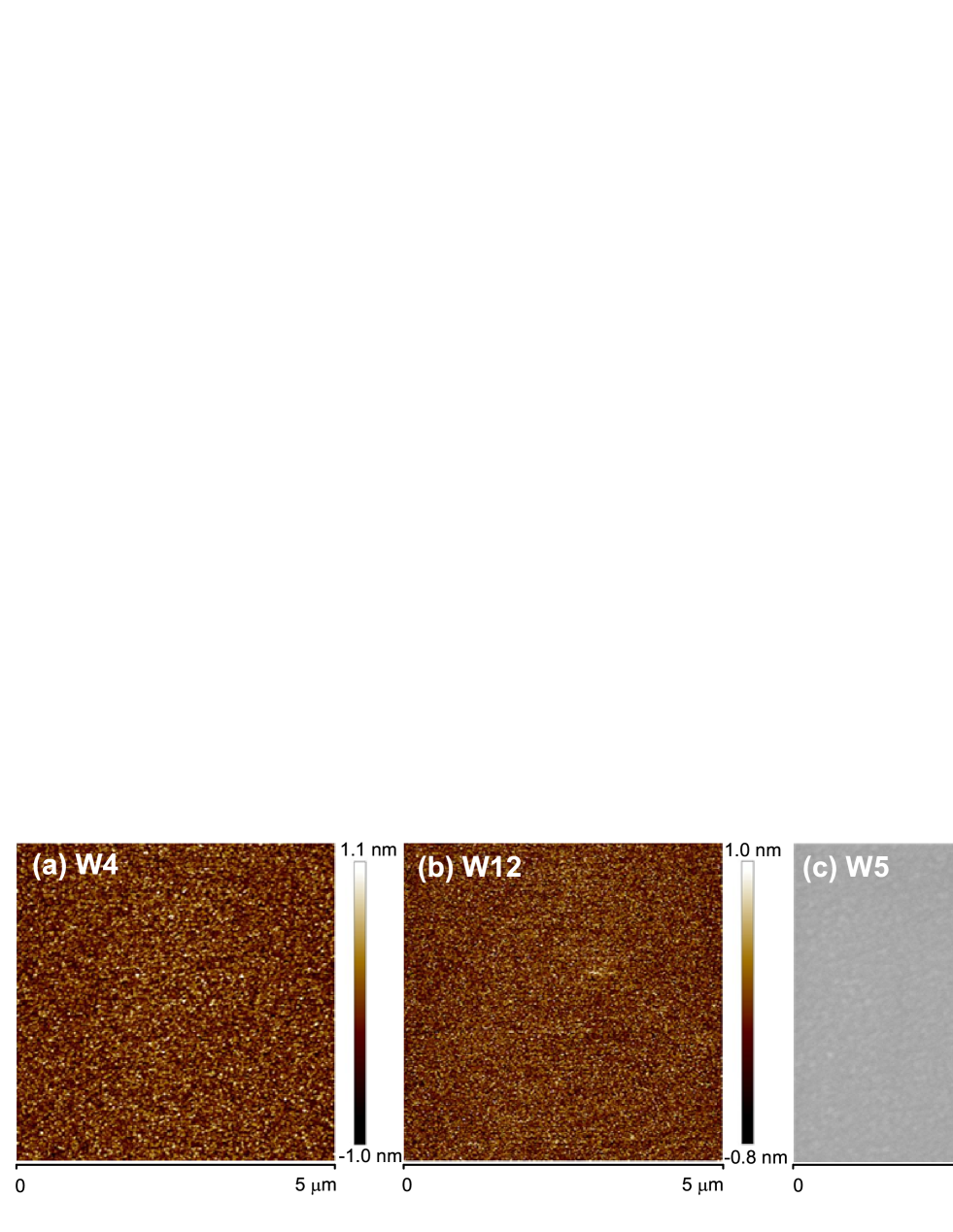
Eight samples grown under different conditions are investigated in this work. The surface morphologies of the films were measured by AFM. All the films show a root-mean-square roughness() of less than 0.3 nm at the scan size of 5 m, indicating a high level of flatness in our samples. As an example, we show the AFM images of two samples W4 and W12 in Figs. 1(a) and (b), respectively. It can be seen that the size of the film grain is about 20 nm with a uniform distribution. In addition, we used a scanning electron microscope to observe the surface topography of the film at a magnification of 160k, see Fig. 1(c). The AFM and SEM images of other samples can be seen Figs. S1, S2 and S3 in the Supplementary Material (SM), both of which reveal the smooth and dense surface of the samples.
To get information about the thickness () of the films, we carried out the X-ray reflectivity measurements. The reflection curve was analyzed using LEPTOS software from Bruker. By constructing a simple three-layer structure model of silicon substrate, NbN film, and the niobium oxide layer, the theoretical curve is obtained to fit with the measured reflection curve, which is presented by the dashed lines in Fig. 1(d). The XRR data of other samples are shown in Fig. S4. The obtained values of film thickness are listed in Table 1.
3.2 Superconducting transition
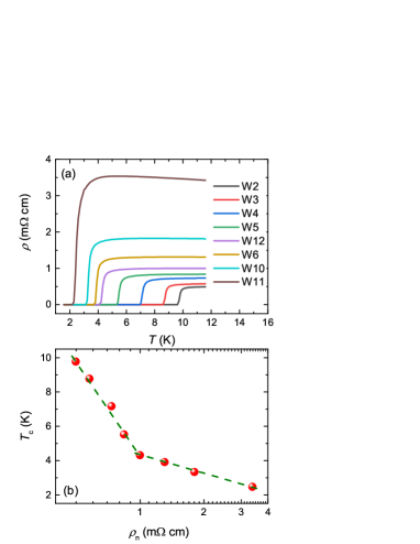
Physical properties of the films in both the superconducting and normal states are studied by the electrical transport measurements. Fig. 2(a) shows the temperature dependent resistivity of the eight films. Sharp SC transitions occurred in the low temperature region. The SC critical temperature reveals a systematical decrease with the increase of N2 content and/or the chamber pressure. Meanwhile, the magnitudes of resistivity in the normal-state also show a systematical evolution. In order to unveil the correlation between the SC and normal-state properties, we plot as a function of in Fig. 2(b). Here is determined using the criteria of 50% to eliminate the effect of SC fluctuation near the onset of the SC transition. is the resistivity in the normal state at 14 K, which is slightly above . It is clear that shows a linear dependence with logarithm of with a change in the slope at round = 1 m cm.
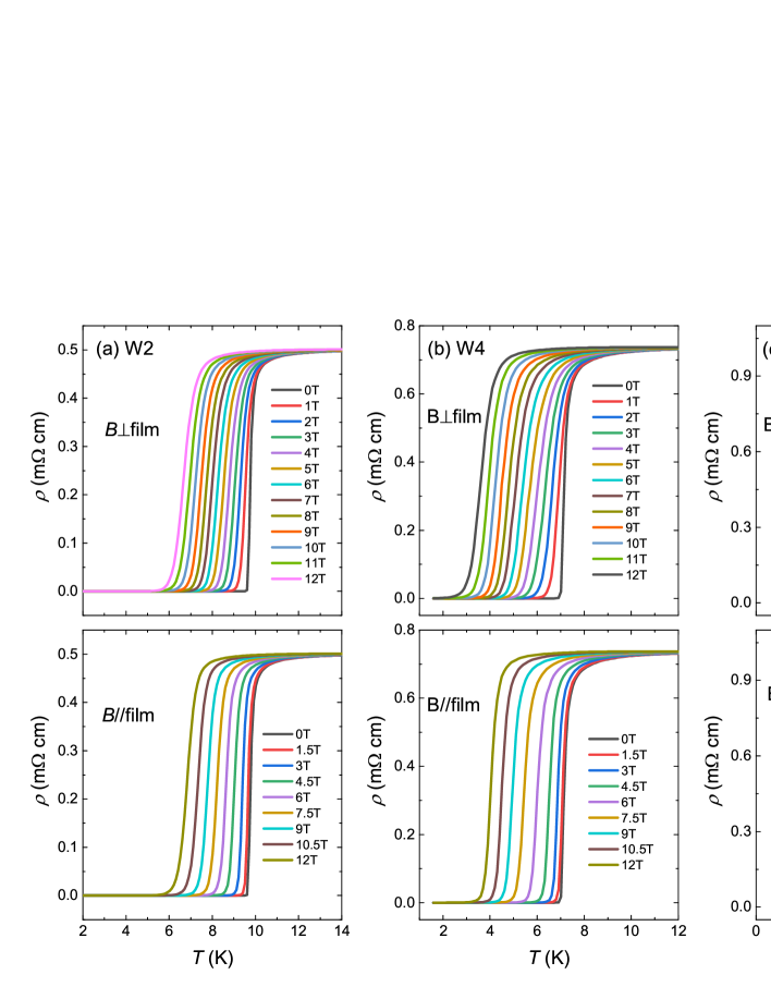
The behaviors of electrical transport under external magnetic field can supply very important information about field induced pair-breaking effect. In Fig. 3, we show temperature-dependent resistivity with various magnetic fields perpendicular and parallel to the film surface for the three samples. The data of other five samples can be seen in Figs. S5 and S6 in SM. As the magnetic field increases, the SC transition shifts to lower temperatures for all the three samples. The field induced broadening effect is more significant with the vertical field ( film), indicating a more active flux motion in this field orientation. In addition, the degree of suppression of magnetic field on the SC transition shows a certain degree of anisotropy, which will be discussed in the next section.
3.3 Upper critical field
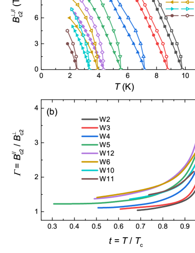
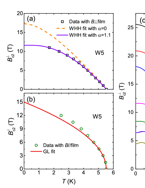
The upper critical fields in the two orientations, and , for all the eight samples as a function of temperature are shown in Fig. 4(a). As we have mentioned, the criteria of 50% is adopted in determining the values of upper critical field. All the samples show the rather large values of the upper critical field, which exceeds the paramagnetic limiting field (= 1.84 , in the unit of T) Clogston (1962). As a demonstration, we show the value of sample W5 in Fig. 4(a), see the red dashed line. For each sample, the value of is always higher than , revealing the clear anisotropic effect in the thin films. In Fig. 4(b), we plot the anisotropic parameter (=) as a function of the reduced temperature . With the decrease of temperature, display a monotonous downward trend. This is similar to that observed in Fe-based superconductors (Fe-based SCs) Wang et al. (2020).
To comprehensively evaluate the influences of the orbital pair-breaking effect, spin-paramagnetic pair-breaking effect, and spin-orbit scattering on the upper critical field, we checked the - data based on the extended WHH theory Werthamer et al. (1966). According to this theory, the upper critical field in the dirty limit can be obtained from the function Werthamer et al. (1966)
| (1) |
where , , and and are parameters reflecting the strength of the spin paramagnetic and spin-orbit scattering, respectively. The parameter is known as Maki parameter Maki (1964). We first show the fitting results of sample W5 as an example. As shown in Fig. 5(a), for the orientation of film, the conventional scenario without spin related pair-breaking effects ( = 0) could not describe the experimental data (see the orange dashed line). By adjusting the values of , the data can be represented by the theoretical model with the parameters = 1.1, as shown by violet dashed line in Fig. 5(a). In this fitting process, the spin-orbit scattering term is fixed to zero. This means that the extended WHH model can describe the experimental data without considering the influence of the spin-orbit scattering in the present system. The data of for all the eight samples is shown in Fig. 5(c). It can be seen that the evolution of with temperature for the eight samples can be described by the extended WHH theory. The obtained Maki parameter is summarized in Fig. 6 and will be discussed in the next section.
In the case of film, as shown in Fig. 5(b), the - data reveals a very steep slope near . Similar behavior has also been observed in ultrathin SC materials de la Barrera et al. (2018); Xi et al. (2016); Lu et al. (2015), which is attributed to the two-dimensional (2D) feature. According to the phenomenological Ginzburg-Landau (GL) model Tinkham (1996), in a 2D system, the upper critical field in the parallel direction should obey the equation
| (2) |
The fitting result is represented by the red dashed line in Fig. 5(b). It can be seen that the 2D GL model can describe the experimental data in the low field region below about 6 T. The deviation between the fitting curve and experimental data in the higher field region is a consequence of the changes in the dimensionality from 2D to 3D due to the decrease of the penetration depth with cooling.
4 Discussion
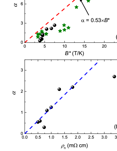
Next, we checked the evolution of Maki parameter with other parameters. According the Maki formula Maki (1964), can be expressed as
| (3) |
where is the upper critical field including only the orbital pair-breaking effect Helfand and Werthamer (1966); Werthamer et al. (1966). Considering the fact that , a simple relation can be obtained Wang et al. (2020). This relation, which is represented by the red dashed line in Fig. 6(a), is compared with the data obtained from the fitting using the extended WHH theory (Eq. 1). The results from the Fe-based SCs Yuan et al. (2009); Kano et al. (2009); Terashima et al. (2009); Lee et al. (2009); Fuchs et al. (2008); Khim et al. (2011); Fang et al. (2010); Khim et al. (2010); Xing et al. (2017); Wang et al. (2017, 2020) are also shown to have a comparison. It is clear that, similar to the behavior of Fe-based system, the data of NbN films also roughly follows the tendency of the Maki formula. The departure of the data from the red dashed line has been attributed to the enhancement of due to the strong-coupling effect. The similarity between the present NbN films and Fe-based SCs indicates that the two systems share a similar strength of SC coupling. An important difference between the two systems is the field orientation: the Pauli paramagnetic effect and the related Maki parameter are observed in the in-plane field direction in Fe-based SCs, while this effect emerges in the perpendicular direction in the NbN films.
In the dirty limit, the value of is proportional to the if the normal state electronic specific heat coefficient has no much change Werthamer et al. (1966). In Fig. 6(b), we show the data of as a function of . Roughly speaking, reveals a linear dependence with as exhibited by the blue dashed line. Sample W11 depart clearly from this linear tendency. This behavior may suggest that the values of is not a constant among these samples. It is notable that the value of covers a wide range (0.5-3.4 m cm), which is clearly larger than that of the single crystals of most sub-systems of Fe-base SCs Wang et al. (2020); Fang et al. (2009); Mu et al. (2009, 2010). Considering the close correlation between and , we argue that the Pauli paramagnetic effect in the present NbN system originates from the enhanced normal-state resistivity.
The dimensional effect in the investigated thin films is another issue worthy of discussion. In principal, dimensional effect can emerges with the decrease of film thickness Tinkham (1996). When the thickness is smaller than the penetration depth , the film can be penetrated by the parallel field, leading to reduction of the diamagnetic energy as compared with the bulk superconductors. In a film much thinner than the out-of-film coherence length , the SC order parameter will not vary appreciably over the film. An estimation from the upper critical field shows that the value of is no more than 10 nm in a wide temperature region, see Fig. S7 in SM. The previous investigations have found that is on the order of several hundred nanometers Pambianchi et al. (1994); Kawakami et al. (2004). Thus, the thickness of the NbN films in this study (20-30 nm) is in the range . As can be seen in Fig. 5(b), the - data can be described by the 2D GL model in the temperature range above 4.3 K. Moreover, the anisotropic parameter is below 3 for W5, see Fig. 4(b). This is also different from the conventional 2D systems with a large anisotropy. The superconducting performances in the thin films with the thickness in this intermediate range is a subject worth studying in the future.
5 Conclusions
In summary, we studied the upper critical field of high-quality NbN thin films, who’s critical temperature and normal-state resistivity were tuned systematically by controlling the growth conditions. The temperature dependence of can be well described by the extended WHH theory, revealing the presence of Pauli paramagnetic effect in this system. The - data near is consistent with the 2D GL model. The Maki parameter shows a clear correlation with and . The large magnitude of may explain the observation of Pauli paramagnetic effect in the present system.
Data availability statement
The data that support the findings of this study are available upon reasonable request from the authors.
Acknowledgments
This work is supported by the National Natural Science Foundation of China (No. 92065116), the Shanghai Technology Innovation Action Plan Integrated Circuit Technology Support Program (No. 22DZ1100200), and the Key-Area Research and Development Program of Guangdong Province, China (No. 2020B0303030002). The authors would like to thank all the staff at the Superconducting Electronics Facility (SELF) for their assistance.
Supplementary Material
The supplementary material is available online at http://xxx.
References
- Keskar et al. (1971) K. S. Keskar, T. Yamashita, and Y. Onodera, :Tap. J. Appl. Phys. 10, 370 (1971).
- Oya and Onodera (1974) G. Oya and Y. Onodera, J. Appl. Phys. 45, 1389 (1974).
- Wang et al. (1996) Z. Wang, A. Kawakami, Y. Uzawa, and B. Komiyama, J. Appl. Phys. 79, 7837 (1996).
- Zhang et al. (2017) W. Zhang, L. Y. You, H. Li, J. Huang, C. Lv, L. Zhang, X. Liu, J. Wu, Z. Wang, and X. Xie, Sci. China-Phys. Mech. Astron. 60, 120314 (2017).
- Liu et al. (2017) Q. Liu, H. Wang, Q. Zhang, J. Ren, W. Peng, and Z. Wang, IEEE T. Appl. Supercon. 27, 1 (2017).
- Shaikhaidarov et al. (2022) R. S. Shaikhaidarov, K. H. Kim1, J. W. Dunstan, I. V. Antonov, S. Linzen, M. Ziegler, D. S. Golubev, V. N. Antonov, E. V. Il’ichev, and Q. V. Astafiev, Nature 608, 45 (2022).
- Chockalingam et al. (2008) S. P. Chockalingam, M. Chand, J. Jesudasan, V. Tripathi, and P. Raychaudhuri, Phys. Rev. B 77, 214503 (2008).
- Joshi et al. (2018) L. M. Joshi, A. Verma, A. Gupta, P. K. Rout, S. Husale, and R. C. Budhani, AIP Advances 8, 055305 (2018).
- Maki (1964) K. Maki, Physics Physique Fizika 1, 127 (1964).
- Maki (1966) K. Maki, Phys. Rev. 148, 362 (1966).
- Helfand and Werthamer (1966) E. Helfand and N. R. Werthamer, Phys. Rev. 147, 288 (1966).
- Werthamer et al. (1966) N. R. Werthamer, E. Helfand, and P. C. Hohenberg, Phys. Rev. 147, 295 (1966).
- Clogston (1962) A. M. Clogston, Phys. Rev. Lett. 9, 266 (1962).
- Wang et al. (2020) T. Wang, C. Zhang, L. C. Xu, J. H. Wang, S. Jiang, Z. W. Zhu, Z. S. Wang, J. N. Chu, J. X. Feng, L. L. Wang, et al., Sci. China-Phys. Mech. Astron. 63, 227412 (2020).
- de la Barrera et al. (2018) S. C. de la Barrera, M. R. Sinko, D. P. Gopalan, N. Sivadas, K. L. Seyler, K. Watanabe, T. Taniguchi, A. W. Tsen, X. Xu, D. Xiao, et al., Nat. Commun. 9, 1427 (2018).
- Xi et al. (2016) X. Xi, ZefangWang, W. Zhao, J.-H. Park, K. T. Law, H. Berger, L. Forro, J. Shan, and K. F. Mak, Nat. Phys. 12, 139 (2016).
- Lu et al. (2015) J. M. Lu, O. Zheliuk, I. Leermakers, N. F. Q. Yuan, U. Zeitler, K. T. Law, and J. T. Ye, Science 350, 1353 (2015).
- Tinkham (1996) M. Tinkham, Introduction to Superconductivity (McGraw-Hill, New York, 1996).
- Yuan et al. (2009) H. Q. Yuan, J. Singleton, F. F. Balakirev, S. A. Baily, G. F. Chen, J. L. Luo, and N. L. Wang, Nature 457, 565 (2009).
- Kano et al. (2009) M. Kano, Y. Kohama, D. Graf, F. Balakirev, A. S. Sefat, M. A. Mcguire, B. C. Sales, D. Mandrus, and S. W. Tozer, J. Phys. Soc. Jpn. 78, 084719 (2009).
- Terashima et al. (2009) T. Terashima, M. Kimata, H. Satsukawa, A. Harada, K. Hazama, S. Uji, H. Harima, G.-F. Chen, J.-L. Luo, and N.-L. Wang, J. Phys. Soc. Jpn. 78, 063702 (2009).
- Lee et al. (2009) H.-S. Lee, M. Bartkowiak, J.-H. Park, J.-Y. Lee, J.-Y. Kim, N.-H. Sung, B. K. Cho, C.-U. Jung, J. S. Kim, and H.-J. Lee, Phys. Rev. B 80, 144512 (2009).
- Fuchs et al. (2008) G. Fuchs, S.-L. Drechsler, N. Kozlova, G. Behr, A. Köhler, J. Werner, K. Nenkov, R. Klingeler, J. Hamann-Borrero, C. Hess, et al., Phys. Rev. Lett. 101, 237003 (2008).
- Khim et al. (2011) S. Khim, B. Lee, J. W. Kim, E. S. Choi, G. R. Stewart, and K. H. Kim, Phys. Rev. B 84, 104502 (2011).
- Fang et al. (2010) M. Fang, J. Yang, F. F. Balakirev, Y. Kohama, J. Singleton, B. Qian, Z. Q. Mao, H. Wang, and H. Q. Yuan, Phys. Rev. B 81, 020509 (2010).
- Khim et al. (2010) S. Khim, J. W. Kim, E. S. Choi, Y. Bang, M. Nohara, H. Takagi, and K. H. Kim, Phys. Rev. B 81, 184511 (2010).
- Xing et al. (2017) X. Z. Xing, W. Zhou, J. H. Wang, Z. W. Zhu, Y. F. Zhang, N. Zhou, B. Qian, X. F. Xu, and Z. X. Shi, Sci. Rep. 7, 45943 (2017).
- Wang et al. (2017) Z. Wang, J. Yuan, J. Wosnitza, H. Zhou, Y. Huang, K. Jin, F. Zhou, X. Dong, and Z. Zhao, J. Phys.: Condens. Matt. 29, 025701 (2017).
- Fang et al. (2009) L. Fang, P. Cheng, Y. Jia, X. Zhu, H. Luo, G. Mu, C. Gu, and H.-H. Wen, J. Cryst. Growth 311, 358 (2009).
- Mu et al. (2009) G. Mu, H. Luo, Z. Wang, L. Shan, C. Ren, and H.-H. Wen, Phys. Rev. B 79, 174501 (2009).
- Mu et al. (2010) G. Mu, B. Zeng, P. Cheng, Z. Wang, L. Fang, B. Shen, L. Shan, C. Ren, and H.-H. Wen, Chin. Phys. Lett. 27, 037402 (2010).
- Pambianchi et al. (1994) M. S. Pambianchi, S. M. Anlage, E. S. Hellman, E. H. Hartford, M. Bruns, and S. Y. Lee, Appl. Phys. Lett. 64, 244 (1994).
- Kawakami et al. (2004) A. Kawakami, Y. Uzawa, and Z. Wang, Physica C 412-414, 1455 (2004).