Large shift current, Zak phase and unconventional nature in Se and Te
Abstract
Recently, unconventional materials (or obstructed atomic insulators) have attracted much attention owing to the unconventional feature of mismatch between Wannier centers and atomic positions. In this paper, we demonstrate that the trigonal selenium and tellurium host an unconventional nature in both electronic and phonon spectra. In electronic band structures, the band representation (BR) decomposition for occupied bands has to contain the essential BR of , and the real-space invariant is . The Zak phase suggests that the one-dimensional Se/Te chain is a chiral Su-Schrieffer-Heeger chain. The effective magnetism can be induced by states at ends. More importantly, a large shift current is obtained in Se quantum well. In addtion, in phonon spectra, three sets of phonon bands are well separated and assigned to , , and BRs, respectively. Thus, the obstructed phonon states are predicted on the (0001) surface. As the prototypes of unconventional materials in both electronic and phonon spectra, our findings could create much interest in the study of obstructed surface electronic and phonon states in these novel materials.
Introduction.
Although topological quantum chemistry (TQC) Bradlyn et al. (2017); Elcoro et al. (2021); Gao et al. (2022a) and symmetry-indicator classification theory Po et al. (2017); Watanabe et al. (2018); Song et al. (2018); Kruthoff et al. (2017); Peng et al. (2022) have achieved great success in the searching for topological band structures in both nonmagnetic and magnetic crystal materials Vergniory et al. (2019); Zhang et al. (2019); Tang et al. (2019); Xu et al. (2020); Gao et al. (2020); Shi et al. (2021); Nie et al. (2020); Guo et al. (2021, 2022); Nie et al. (2018), a significant proportion of materials are topologically trivial, but host the type I unconventional feature of mismatch between the electronic Wannier centers and atomic positions, which are named as unconventional insulators or obstructed atomic insulators (OAIs) Nie et al. (2021a, b); Gao et al. (2022b); Xu et al. . Among them, various properties have been well studied already, such as electrides Nie et al. (2021a), thermoelectronics Gao et al. (2022b), catalysis Li (2022), electrochemistry Sivula and van de Krol (2016), solid-state hydrogen storage Gao et al. (2022b), ferroelectronics and superconductivity Wu et al. (2022); Reyren et al. (2007); Ohtomo and Hwang (2004). Given an OAI with cleavage terminations cutting through an obstructed Wannier charge center, metallic surface states could possibly exist within the bulk gap, which is referred to as the filling anomaly Benalcazar et al. (2017a, b); Schindler et al. (2019); Xu et al. . Such metallic states on the surface/interface are key to many interesting physical and chemical properties of these unconventional materials Gao et al. (2022b); Xu et al. . On the other hand, the concept of unconventionality can be extended to phonon spectra, when phonon modes are well separated in frequency (by a frequency gap) Zhang et al. (2023). For an unconventional phonon band structure, the surface phonon modes are expected in the frequency gap. So far, no material has been predicted to be unconventional yet in both electronic and phonon band structures.
In this work, we demonstrate that the trigonal selenium and tellurium are unconventional in both electronic and phonon spectra. The essential band representation is ( is an empty site). The real-space invariant (RSI) is computed . The Zak phase suggests that the 1D Se/Te chain is a chiral Su-Schrieffer-Heeger (SSH) chain. The electronic gap can be modified by quantum-well structures, with electrons and holes being at two different interfaces, which yields a large shift current. On the other hand, in their phonon bands, the band representations are assigned to three sets of separated phonon bands by the IR2PH compute phonon-mode irreducible representations with interface to the Quantum ESPRESSO package and UnconvMat packages Gao et al. (2022b); eBR/aBR decomposition: a general workflow to get unconventional band structures ; Gao et al. (2021). Accordingly, the obstructed surface phonon modes are obtained on the (0001) surface. Se and Te are the prototypes of unconventional materials in both electronic and phonon band structures.
| Atom | WKS() | Symm. | Conf. | Irreps() | aBRs() | occ. |
|---|---|---|---|---|---|---|
| Se | : | |||||
| (Te) | () | : | yes | |||
| : | ||||||
| yes | ||||||
Crystal structures and aBR analysis.
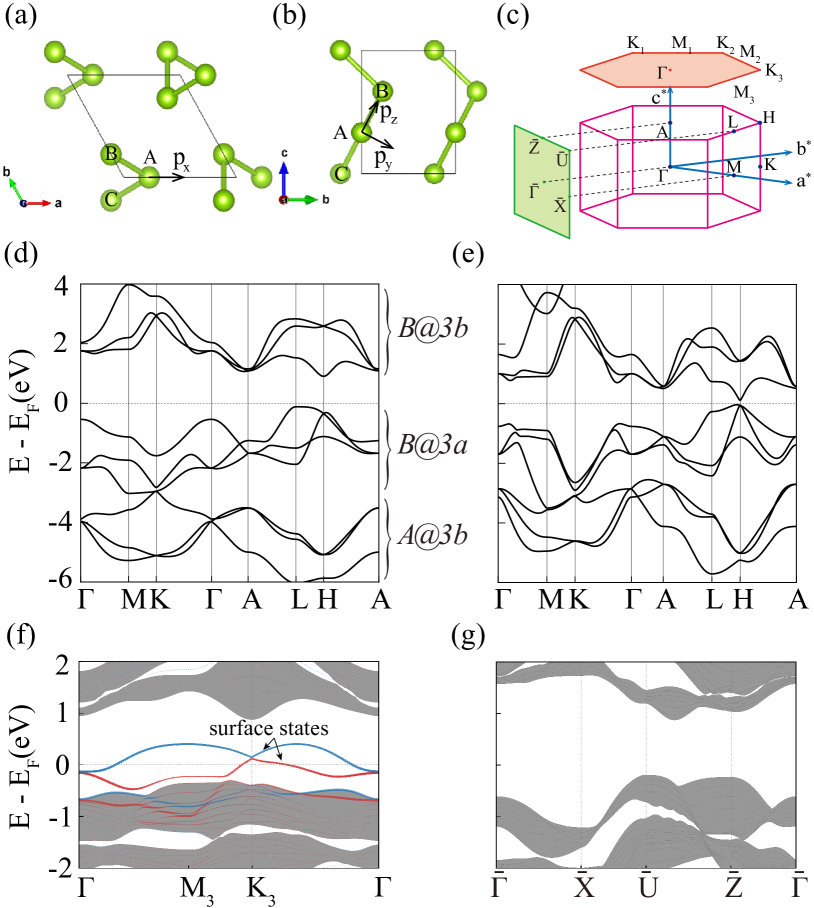
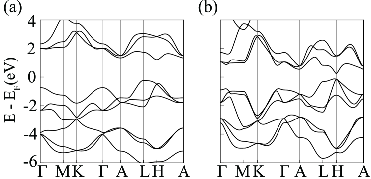
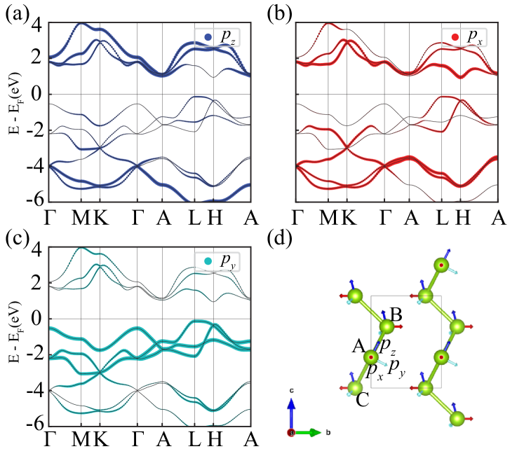
The Se and Te crystals crystallize in the structure of SG 152 (right-handed). The atoms are located the Wyckoff site (WKS; Table 1), and covalently bonded into chiral 1D chains along . The neighboring chains are bonded by van der Waals (vdW) forces in the other two dimensions (i.e., plane) to form a triangular lattice [Fig. 1(a)]. The band structures of Se and Te are presented in Figs. 1(d) and 1(e), indicating an insulating behavior. For more calculation details, please see Appendix A. In the theory of TQC, one can identify the BR () for any isolated set of electronic bands, which tells the Wannier center () and local orbital character (; labeled by site symmetry) Nie et al. (2021a). The atomic valence-electron BRs (aBRs) are tabulated in Table 1. Based on the computed irreducible representations, the aBR decomposition for the occupied bands is solved online Gao et al. (2022b); eBR/aBR decomposition: a general workflow to get unconventional band structures to be , with the essential BR responsible for charge mismatch. The RSI for the empty site is computed to be , where denotes the number of , indicating the unconventional nature of the OAI. The specific orbital-resolved band structures and TB model are provided in Appendix B.
Zak phase and surface states.
With the understanding of the essential BR at , we will expect the metallic state on the top surface while no such state on the side surface. Thus, we have performed the (0001)- and ()-slab calculations. In Fig. 1(f), we clearly see metallic surface states on the (0001) surface. Moreover, we notice that the unconventional nature is closely related to the Zak phase Zak (1989). The Zak phase is defined by the integral of the Berry connection along a reciprocal lattice vector (). In trigonal Se crystals, the Zak phase is defined by
| (1) |
where is the periodic part of the bulk Bloch wave function in the th band, with the gauge choice and . Due to the presence of symmetry on - K/K - M and symmetry on - M, the Zak phase is quantized to be zero or (mod ). The Zak phase along MK is computed, being . Away from the high-symmetry lines, it would slightly vibrate around . The values of the Zak phase correspond to the presence/absence of in-gap boundary states, which are similar to those in the SSH model Rhim et al. (2017) . The 1D Se chains are chiral SSH chains. As shown for the (0001) slab, polarization charges are equal to (mod ) at the ends of the 1D insulating chain. As these chiral SSH chains are vdW interacted, they result in metallic surface states, being consistent with ab-initio calculations.
Quantum wells, interfaces and shift current.
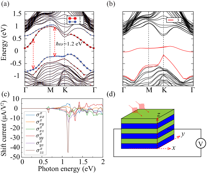
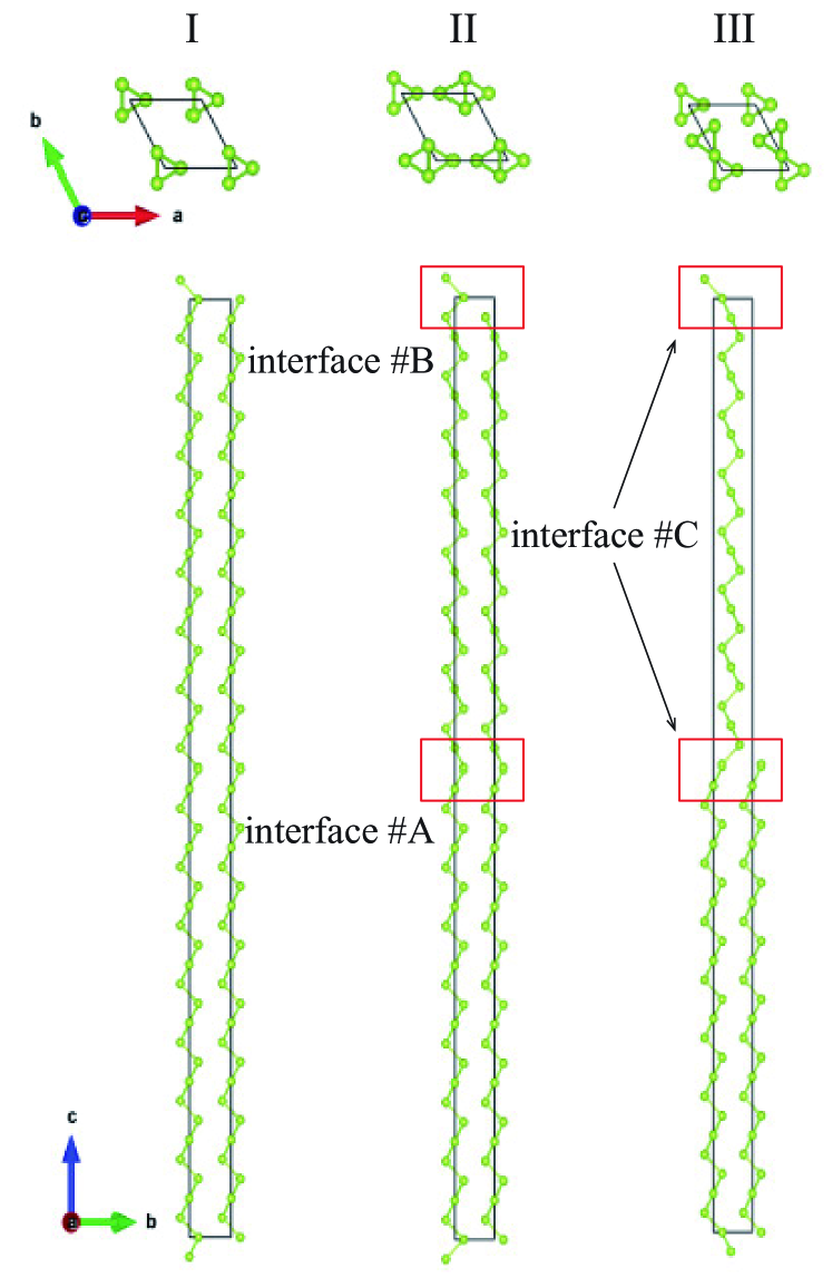
Due to existence of the Zak phase, we can generate in-gap states on different (0001) interfaces, to modify the band gap and properties though the quantum-well structures. Here, we twisted two different chiral structures by 60 degrees to form two interfaces 1 and 2 and 180 degrees to form interfaces 3. We have performed the calculations of two quantum wells (QWs). QW-I contains interfaces 1 and 2, while QW-II has identical interface 3. The top and side views of the structures are given in Fig. 9 in Appendix C. The band structures of the quantum wells are shown in Figs. 2(a) and 2(b). In Fig. 2(b), the flat in-gap interface states are also obtained on interface 3. In Fig. 2(a), the interface states are clearly seen in the bulk gap, and their surface weights have been denoted by the size of the dots for interfaces 1 and 2, respectively. We find that the indirect band gap becomes smaller in the QW-I structure. More surprisingly, electron and hole carriers accumulate at different interfaces, which can prohibit the recombination of electrons and holes.
Thus, we have calculated the shift current of this quantum well. In second-order optical response, a shift current can be generated by an injected linear polarized light via
| (2) |
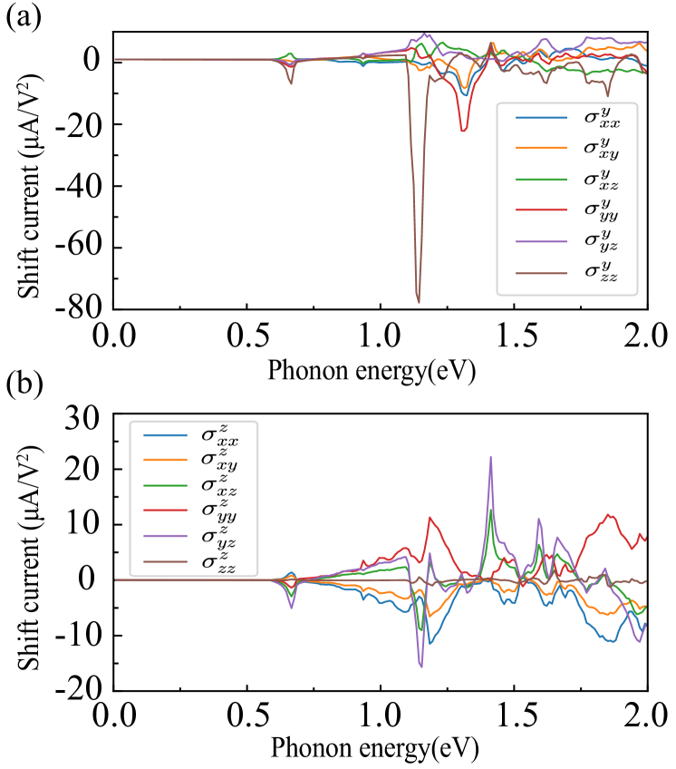
where is electrical field along and the strength of the response can be described by the magnitude of second-order photoconductivity Kraut and von Baltz (1979); Belinicher and Sturman (1980); Sipe and Shkrebtii (2000). The results show a large shift current at in Fig. 2. The response tenser elements corresponding to the shift current along , , and are given in Figs. 2(c), 8(a) and 8(b), respectively. The peak value for the and components can reach up to and , respectively, with a photon energy of . So large photoconductivity is comparable to the record of reported values in semiconductors Young and Rappe (2012); Zheng et al. (2015); Brehm et al. (2014); von Hippel (1950); Shieh et al. (2009); Liu et al. (2017); Côté et al. (2002); Sotome et al. (2019); Tan et al. (2016), making the Se quantum well a promising photodetection device. We further analyzed the origin of the strong response. From the electronic band structure, one can easily find that the bands from two different interfaces (1 and 2) with direct band gaps in a large area [see Fig. 2(a)]. The optical transition between the interfaces 1 and 2 contributes to the peak value of photoconductivity and can generate a strong in-plane shift current via the tenser elements and . The details of the second-order optical conductivity are given in Appendix A.
Magnetism at the ends of the chiral SSH chain.
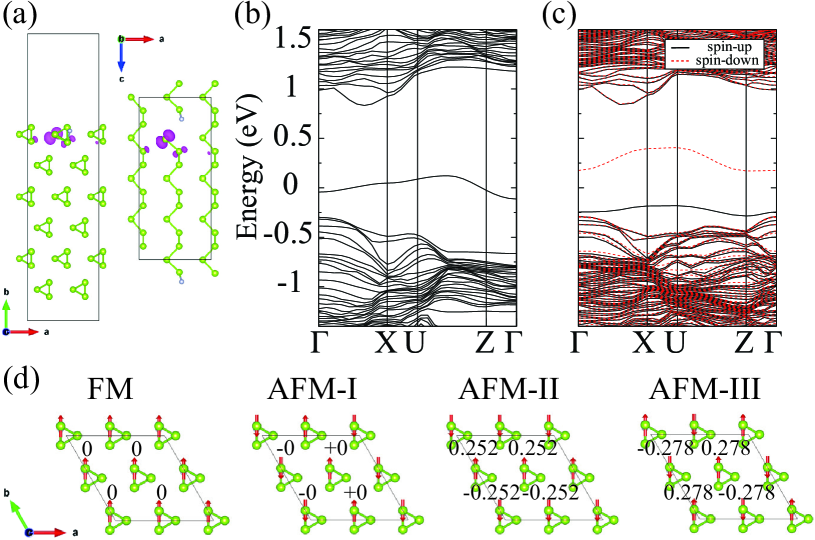
To investigate the magnetic property at the ends of the chiral SSH chain, we induce a vacancy defect on the surface of the () slab and passivate an end by the F atom. The relaxed crystal structure is obtained in Fig. 3(a). The non-spin-polarized and spin-polarized band structures are calculated. In the non-spin-polarized band structure of Fig. 3(b), an isolated state is localized at the end of the chain, being half filling and metallic. The partial charge distribution of this end state is plotted in Fig. 3(a). After considering spin polarization, it becomes insulating with at the end with a lower total energy. The magnetism is induced by the unpaired electron at the end of a SSH chain. The polarized end state is confirmed by the calculations with two (or more) vacancies on a chain to reduce the interaction between the two ends of the chain in the slab structures.
Then we simulate the magnetic ordering on the ideal (0001) termination, which is an arrangement of the ends of the chiral SSH chains. We have performed the calculations for different magnetic configurations in a supercell. The results are shown in Fig. 3(d). We use the energy mapping method to estimate the nearest-neighbor exchange interaction. Here, we consider an Ising-type model,
| (3) |
Because there are three types of nearest-neighbor exchange interactions, the NN can be divided into along , along , and along . We consider one ferromagnetic (FM) and three antiferromagnetic (AFM) configurations, as indicated by the arrows in Fig. 3(d). We find that the FM and AFM-I states converge to paramagnetic states during the self-consistent calculations and the converged magnetic moments in AFM-II and AFM-III states are presented in Fig. 3(d). The converged energies are given in Table 2. According to the Ising-type model, the energies of the Se magnetic configurations can be written as,
| (4) | ||||
We can solve . Then, assuming , we get . As expected, is much less then and these values are consistent with the most stable configuration AFM-III.
| FM | AFM-I | AFM-II | AFM-III | |
|---|---|---|---|---|
| Energy (meV) | 72.38 | 72.38 | 19.08 | 0 |
Unconventional phonon spectra.
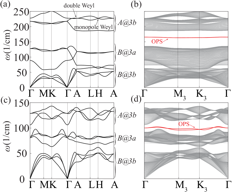
The phonon modes are originated from the vibration of the atoms, which would induce the atomic vibration band representations as the p-orbitals in the phonon spectrum. Similarly, the phonon spectra with a set of separated phonon bands being not a sum of aBRs are defined as the unconventional phonon spectra Zhang et al. (2023). As a result, the obstructed phonon modes emerge on terminations of finite-size samples. The phonon spectra are computed and shown in Fig. 4 for Se and Te respectively. We use IR2PH to deal with the phonon modes from the DFPT calculations and obtain the irreps compute phonon-mode irreducible representations with interface to the Quantum ESPRESSO package . Through tqc.data, the BR decomposition for each set of phonon bands is solved online eBR/aBR decomposition: a general workflow to get unconventional band structures , as shown in Figs. 4(a) and 4(c). As expected, the obstructed phonon states are obtained in Figs. 4(b) and 4(d). Based on the full list of symmetry-protected Weyl phonons in Ref. Liu et al. (2020), the depicted A and H points are double and monopole Weyl points, respectively. The arc states of Weyl points are shown in Fig. 10 in Appendix D.
Discussion.
In summary, we present that the trigonal Se and Te are unconventional elements in both electronic and phonon spectra. The essential BR of the occupied electronic bands is and it is characterized by a nonzero RSI . Since site is the center of bonds in the 1D chiral Se/Te chain in the direction ( Zak phase), the metallic in-gap states are obtained on the (0001) surfaces and interfaces. Noting that the topological property of the Se/Te chain was investigated very recently Kłosiński et al. (2023). As semiconductors, the band gap can be modified by the quantum-well structure with electrons and holes being at two different interfaces, which benefits to the application of the solar cells. A super-high shift current is obtained in the quantum well. Additionally, based on the BR decomposition of the phonon bands, we conclude that the phonon bands are unconventional and the obstructed surface phonon modes are obtained on the (0001) surface/interface. As the prototypes of a novel kind of materials with both electronic and phonon unconventional band structures, our study can create future interest in the study of surface charge and phonons in these kind of materials.
Acknowledgments.
We thank Dr. Qing-Bo Liu for finding the Weyl points and calculating surface arc states of the Se phonon spectrum. This work was supported by the National Key R&D Program of China (Grant No. 2022YFA1403800), National Natural Science Foundation of China (Grants No. 11974395, No. 12188101 and No. 52188101), the Strategic Priority Research Program of Chinese Academy of Sciences (Grant No. XDB33000000), the China Postdoctoral Science Foundation funded project (Grant No. 2021M703461), and the Center for Materials Genome.
References
- Bradlyn et al. (2017) Barry Bradlyn et al., “Topological quantum chemistry,” Nature 547, 298–305 (2017).
- Elcoro et al. (2021) Luis Elcoro, Benjamin J. Wieder, Zhida Song, Yuanfeng Xu, Barry Bradlyn, and B. Andrei Bernevig, “Magnetic topological quantum chemistry,” Nat. Commun. 12, 5965 (2021).
- Gao et al. (2022a) Jiacheng Gao, Zhaopeng Guo, Hongming Weng, and Zhijun Wang, “Magnetic band representations, fu-kane-like symmetry indicators, and magnetic topological materials,” Phys. Rev. B 106, 035150 (2022a).
- Po et al. (2017) Hoi Chun Po, Ashvin Vishwanath, and Haruki Watanabe, “Symmetry-based indicators of band topology in the 230 space groups,” Nat. Commun. 8, 50 (2017).
- Watanabe et al. (2018) Haruki Watanabe, Hoi Chun Po, and Ashvin Vishwanath, “Structure and topology of band structures in the 1651 magnetic space groups,” Sci. Adv. 4, eaat8685 (2018).
- Song et al. (2018) Zhida Song, Tiantian Zhang, Zhong Fang, and Chen Fang, “Quantitative mappings between symmetry and topology in solids,” Nat. Commun. 9, 3530 (2018).
- Kruthoff et al. (2017) Jorrit Kruthoff, Jan de Boer, Jasper van Wezel, Charles L. Kane, and Robert-Jan Slager, “Topological classification of crystalline insulators through band structure combinatorics,” Phys. Rev. X 7, 041069 (2017).
- Peng et al. (2022) Bingrui Peng, Yi Jiang, Zhong Fang, Hongming Weng, and Chen Fang, “Topological classification and diagnosis in magnetically ordered electronic materials,” Phys. Rev. B 105, 235138 (2022).
- Vergniory et al. (2019) M. G. Vergniory, L. Elcoro, Claudia Felser, Nicolas Regnault, B. Andrei Bernevig, and Zhijun Wang, “A complete catalogue of high-quality topological materials,” Nature 566, 480–485 (2019).
- Zhang et al. (2019) Tiantian Zhang et al., “Catalogue of topological electronic materials,” Nature 566, 475–479 (2019).
- Tang et al. (2019) Feng Tang, Hoi Chun Po, Ashvin Vishwanath, and Xiangang Wan, “Comprehensive search for topological materials using symmetry indicators,” Nature 566, 486–489 (2019).
- Xu et al. (2020) Yuanfeng Xu et al., “High-throughput calculations of magnetic topological materials,” Nature 586, 702–707 (2020).
- Gao et al. (2020) Jiacheng Gao, Shiyu Peng, Zhijun Wang, Chen Fang, and Hongming Weng, “Electronic structures and topological properties in nickelates ,” Nat. Sci. Rev. 8 (2020).
- Shi et al. (2021) Wujun Shi et al., “A charge-density-wave topological semimetal,” Nat. Phys. 17, 381–387 (2021).
- Nie et al. (2020) Simin Nie, Yan Sun, Fritz B. Prinz, Zhijun Wang, Hongming Weng, Zhong Fang, and Xi Dai, “Magnetic semimetals and quantized anomalous hall effect in ,” Phys. Rev. Lett. 124, 076403 (2020).
- Guo et al. (2021) Zhaopeng Guo, Dayu Yan, Haohao Sheng, Simin Nie, Youguo Shi, and Zhijun Wang, “Quantum spin hall effect in ,” Phys. Rev. B 103, 115145 (2021).
- Guo et al. (2022) Z. Guo, J. Deng, Y. Xie, and Z. Wang, “Quadrupole topological insulators in monolayers,” NPJ Quantum Mater. 7, 87 (2022).
- Nie et al. (2018) Simin Nie, Lingyi Xing, Rongying Jin, Weiwei Xie, Zhijun Wang, and Fritz B. Prinz, “Topological phases in the compound,” Phys. Rev. B 98, 125143 (2018).
- Nie et al. (2021a) Simin Nie, Yuting Qian, Jiacheng Gao, Zhong Fang, Hongming Weng, and Zhijun Wang, “Application of topological quantum chemistry in electrides,” Phys. Rev. B 103, 205133 (2021a).
- Nie et al. (2021b) Simin Nie, B. Andrei Bernevig, and Zhijun Wang, “Sixfold excitations in electrides,” Phys. Rev. Research 3, L012028 (2021b).
- Gao et al. (2022b) Jiacheng Gao et al., “Unconventional materials: the mismatch between electronic charge centers and atomic positions,” Sci. Bull. 67, 598–608 (2022b).
- (22) Yuanfeng Xu et al., “Three-Dimensional Real Space Invariants, Obstructed Atomic Insulators and A New Principle for Active Catalytic Sites,” arXiv:2111.02433 .
- Li (2022) Guowei et al. Li, “Obstructed surface states as the descriptor for predicting catalytic active sites in inorganic crystalline materials,” Adv. Mater. 34, 2201328 (2022).
- Sivula and van de Krol (2016) Kevin Sivula and Roel van de Krol, “Semiconducting materials for photoelectrochemical energy conversion,” Nat. Rev. Mater. 1, 15010 (2016).
- Wu et al. (2022) Heng Wu et al., “The field-free josephson diode in a van der waals heterostructure,” Nature 604, 653–656 (2022).
- Reyren et al. (2007) N. Reyren et al., “Superconducting interfaces between insulating oxides,” Science 317, 1196–1199 (2007).
- Ohtomo and Hwang (2004) A. Ohtomo and H. Y. Hwang, “A high-mobility electron gas at the heterointerface,” Nature 427, 423–426 (2004).
- Benalcazar et al. (2017a) Wladimir A. Benalcazar, B. Andrei Bernevig, and Taylor L. Hughes, “Quantized electric multipole insulators,” Science 357, 61–66 (2017a).
- Benalcazar et al. (2017b) Wladimir A. Benalcazar, B. Andrei Bernevig, and Taylor L. Hughes, “Electric multipole moments, topological multipole moment pumping, and chiral hinge states in crystalline insulators,” Phys. Rev. B 96, 245115 (2017b).
- Schindler et al. (2019) Frank Schindler, Marta Brzezińska, Wladimir A. Benalcazar, Mikel Iraola, Adrien Bouhon, Stepan S. Tsirkin, Maia G. Vergniory, and Titus Neupert, “Fractional corner charges in spin-orbit coupled crystals,” Phys. Rev. Research 1, 033074 (2019).
- (31) Yuanfeng Xu et al., “Filling-Enforced Obstructed Atomic Insulators,” arXiv:2106.10276 .
- Zhang et al. (2023) Ruihan Zhang, Haohao Sheng, Junze Deng, Zhilong Yang, and Zhijun Wang, “Unconventional phonon spectra and obstructed edge phonon modes,” (2023), arXiv:2305.09453 [cond-mat.mtrl-sci] .
- (33) To compute phonon-mode irreducible representations with interface to the Quantum ESPRESSO package, https://github.com/zjwang11/ir2pw. .
- (34) eBR/aBR decomposition: a general workflow to get unconventional band structures, http://tm.iphy.ac.cn/UnconvMat.html .
- Gao et al. (2021) Jiacheng Gao, Quansheng Wu, Clas Persson, and Zhijun Wang, “Irvsp: To obtain irreducible representations of electronic states in the VASP,” Comput. Phys. Commun. 261, 107760 (2021).
- Zak (1989) J. Zak, “Berry’s phase for energy bands in solids,” Phys. Rev. Lett. 62, 2747–2750 (1989).
- Rhim et al. (2017) Jun-Won Rhim, Jan Behrends, and Jens H. Bardarson, “Bulk-boundary correspondence from the intercellular zak phase,” Phys. Rev. B 95, 035421 (2017).
- Kraut and von Baltz (1979) Wolfgang Kraut and Ralph von Baltz, “Anomalous bulk photovoltaic effect in ferroelectrics: A quadratic response theory,” Phys. Rev. B 19, 1548–1554 (1979).
- Belinicher and Sturman (1980) V I Belinicher and B I Sturman, “The photogalvanic effect in media lacking a center of symmetry,” Sov. Phys. Usp. 23, 199–223 (1980).
- Sipe and Shkrebtii (2000) J. E. Sipe and A. I. Shkrebtii, “Second-order optical response in semiconductors,” Phys. Rev. B 61, 5337–5352 (2000).
- Young and Rappe (2012) Steve M. Young and Andrew M. Rappe, “First principles calculation of the shift current photovoltaic effect in ferroelectrics,” Phys. Rev. Lett. 109, 116601 (2012).
- Zheng et al. (2015) Fan Zheng, Hiroyuki Takenaka, Fenggong Wang, Nathan Z. Koocher, and Andrew M. Rappe, “First-principles calculation of the bulk photovoltaic effect in and ,” J. Phys. Chem. Lett. 6, 31–37 (2015).
- Brehm et al. (2014) John A. Brehm, Steve M. Young, Fan Zheng, and Andrew M. Rappe, “First-principles calculation of the bulk photovoltaic effect in the polar compounds and ,” J. Chem. Phys. 141, 204704 (2014).
- von Hippel (1950) A. von Hippel, “Ferroelectricity, domain structure, and phase transitions of barium titanate,” Rev. Mod. Phys. 22, 221–237 (1950).
- Shieh et al. (2009) J. Shieh, J.H. Yeh, Y.C. Shu, and J.H. Yen, “Hysteresis behaviors of barium titanate single crystals based on the operation of multiple switching systems,” Mater. Sci. Eng. B 161, 50–54 (2009).
- Liu et al. (2017) Shi Liu, Fan Zheng, and Andrew M. Rappe, “Giant bulk photovoltaic effect in vinylene-linked hybrid heterocyclic polymer,” J. Phys. Chem. C 121, 6500–6507 (2017).
- Côté et al. (2002) D. Côté, N. Laman, and H. M. van Driel, “Rectification and shift currents in gaas,” Appl. Phys. Lett. 80, 905–907 (2002).
- Sotome et al. (2019) M. Sotome et al., “Spectral dynamics of shift current in ferroelectric semiconductor sbsi,” Proc. Natl Acad. Sci. 116, 1929–1933 (2019).
- Tan et al. (2016) Liang Z Tan, Fan Zheng, Steve M Young, Fenggong Wang, Shi Liu, and Andrew M Rappe, “Shift current bulk photovoltaic effect in polar materials—hybrid and oxide perovskites and beyond,” NPJ Comput. Mater. 2, 16026 (2016).
- Liu et al. (2020) Qing-Bo Liu, Yuting Qian, Hua-Hua Fu, and Zhijun Wang, “Symmetry-enforced Weyl phonons,” NPJ Comput. Mater. 6, 95 (2020).
- Kłosiński et al. (2023) Adam Kłosiński, Wojciech Brzezicki, Alexander Lau, Cliò E. Agrapidis, Andrzej M. Oleś, Jasper van Wezel, and Krzysztof Wohlfeld, “Topology of chalcogen chains,” Phys. Rev. B 107, 125123 (2023).
- Tran and Blaha (2009) Fabien Tran and Peter Blaha, “Accurate band gaps of semiconductors and insulators with a semilocal exchange-correlation potential,” Phys. Rev. Lett. 102, 226401 (2009).
- Becke and Johnson (2006) Axel D. Becke and Erin R. Johnson, “A simple effective potential for exchange,” J. Chem. Phys. 124, 221101 (2006).
- Giannozzi et al. (2009) Paolo Giannozzi et al., “QUANTUM ESPRESSO: a modular and open-source software project for quantum simulations of materials,” J. Phys. Condens. Matter 21, 395502 (2009).
- Giannozzi et al. (2017) P Giannozzi et al., “Advanced capabilities for materials modelling with quantum ESPRESSO,” J. Phys. Condens. Matter 29, 465901 (2017).
- Blöchl (1994) P. E. Blöchl, “Projector augmented-wave method,” Phys. Rev. B 50, 17953–17979 (1994).
- Kresse and Joubert (1999) G. Kresse and D. Joubert, “From ultrasoft pseudopotentials to the projector augmented-wave method,” Phys. Rev. B 59, 1758–1775 (1999).
- Perdew et al. (1996) John P. Perdew, Kieron Burke, and Matthias Ernzerhof, “Generalized gradient approximation made simple,” Phys. Rev. Lett. 77, 3865–3868 (1996).
- Slater and Koster (1954) J. C. Slater and G. F. Koster, “Simplified LCAO method for the periodic potential problem,” Phys. Rev. 94, 1498–1524 (1954).
Appendix
A CRYSTAL STRUCTURE AND CALCULATION METHODS
The elementary substances Se and Te (SG 152, ) host a hexagonal lattice (parameters along , respectively), whose atoms located at Wyckoff positions , i.e., , , and , forming a right-handed trigonal helix along . The parameters are Å Å for Te and Å Å for Se. The modified Becke Johnson (MBJ) band structures of Se and Te are presented in Figs. 5(a) and 5(b) Tran and Blaha (2009); Becke and Johnson (2006) .
We performed the first-principles calculations based on the density functional theory (DFT) implemented in the Quantum ESPRESSO package Giannozzi et al. (2009, 2017), using the projector augmented-wave (PAW) method Blöchl (1994); Kresse and Joubert (1999). The electrons are described using the generalized gradient approximation (GGA) with exchange-correlation functional of Perdew, Burke and Ernzerhof (PBE) Perdew et al. (1996) for the exchange-correlation functional. The plane-wave cutoff energy was set to 70 Ry. The thickness of the vacuum layer along axis was set to Å. The lattice dynamical properties are described using the GGA with exchange-correlation functional of PBE for the exchange-correlation functional. The plane-wave cutoff energy was set to 50 Ry. The phonon calculations are performed in the framework of density functional perturbation theory, as implemented in the Quantum ESPRESSO package.
The irreducible representations of electronic states and phonon modes were computed by our homemade programs IR2PW and IR2PH, respectively. They are released on Github compute phonon-mode irreducible representations with interface to the Quantum ESPRESSO package .
The same band topology, we mainly focus on the discussion of Se in the main text hereafter.
It is physically different from that of the p-n junction mechanism. In bulk optical response, the linear response can be understood as , where is the first-order optical conductivity. A current along the a direction can be generated by the applied optical-electrical filed along the b direction. One can see that and are with the same frequency; therefore, the bulk photovoltaic effect is forbidden in the first-order response and dominated by the second-order response. The bulk photovoltaic effect can be considered as a joint effect of the frequency-dependent density of states and the wave function.
We calculate the second-order optical conductivity by
| (5) | ||||
where and are band indices, is the Fermi-Dirac distribution difference, is the interband Berry connection, the term relates to the mediate virtual states, and is the energy difference. We deal with the delta function by a Gauss distribution with a smearing factor of 0.01eV.
B ORBITAL-RESOLVED BAND STRUCTURES AND TB MODEL
The orientations of the defined local orbitals at each Se atoms according to site symmetry are presented in Fig. 6(d). The orbital-resolved band with respect to this orbital setup are shown in Figs. 6(a)–(c), from which we can find that the defined orbitals are fully occupied forming the aBR .
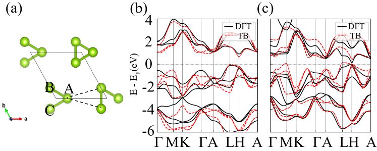
Though the Slater-Koster method Slater and Koster (1954), the band structures can be well reproduced by a orbital tight-binding (TB) model with two kinds of bonds: the nearest-neighbor (NN) bonds and the next-nearest-neighbor (NNN) bonds in Fig. 7. Their and parameters are given in Table 3. The band structures of the TB model are given in in Fig. 7.
| Atom | ||||
|---|---|---|---|---|
| Se | ||||
| Te |
C LARGE SHIFT CURRENT AND QUANTUM WELLS
D WEYL POINTS AND SURFACE STATES IN PHONON SPECTRUM
The Weyl points between 8th and 9th phonon bands in the phonon spectrum of Se are listed in Table 4. The corresponding surface/arc states are obtained in Fig. 10 for (0001) surface.
| Weyl points | Loc. (fractional) | Freq. () | Charge | Deg. |
|---|---|---|---|---|
| WP1 | ||||
| WP2 | ||||
| WP3 | ||||
| WP4 |