DeepFlow: A Cross-Stack Pathfinding Framework for Distributed AI Systems
Abstract
Over the past decade, machine learning model complexity has grown at an extraordinary rate, as has the scale of the systems training such large models. However there is an alarmingly low hardware utilization (5-20%) in large scale AI systems. The low system utilization is a cumulative effect of minor losses across different layers of the stack, exacerbated by the disconnect between engineers designing different layers spanning across different industries. We propose CrossFlow, a novel framework that enables cross-layer analysis all the way from the technology layer to the algorithmic layer. We also propose DeepFlow (built on top of CrossFlow using machine learning techniques) to automate the design space exploration and co-optimization across different layers of the stack. We have validated CrossFlow accuracy with distributed training on real commercial hardware and showcase several DeepFlow case studies demonstrating pitfalls of not optimizing across the technology-hardware-software stack for what is likely, the most important workload driving large development investments in all aspects of computing stack.
1 Introduction
Over the last decade, the demand on compute and memory resources for AI workloads has grown by multiple orders of magnitude [1]. As AI models grow in size along with the volume of training data, distributed training on cutting-edge scale-out systems composed of a large number of accelerators and processors has become the norm. However, it has often been noticed that large scale AI training suffers from poor resource utilization. E.g., recent analysis reveals 5-20% utilization across 1000s of GPUs [2]. Such poor utilization of resources is becoming a source of major concern. Inefficiencies across different layers of the compute stack [3, 4] (from hardware micro-architecture to software parallelization strategies) and the design imbalance across different layers are among a few factors resulting in such low system utilization. Different layers of the stack, technology nodes, hardware architecture, network topology, model architecture, parallelism strategy are designed across different organizations and retrofitted into the large-scale systems. The distributed nature of the design makes cross-layer optimization challenging if not impossible. For example, high-level design decisions like batch size, model architecture, and parallelism strategy exploited at algorithmic level stress underlying hardware components (network, memory bandwidth or compute units) in different ways which call for different architectural designs, network topologies, memory technologies and technology nodes to ensure high system utilization.
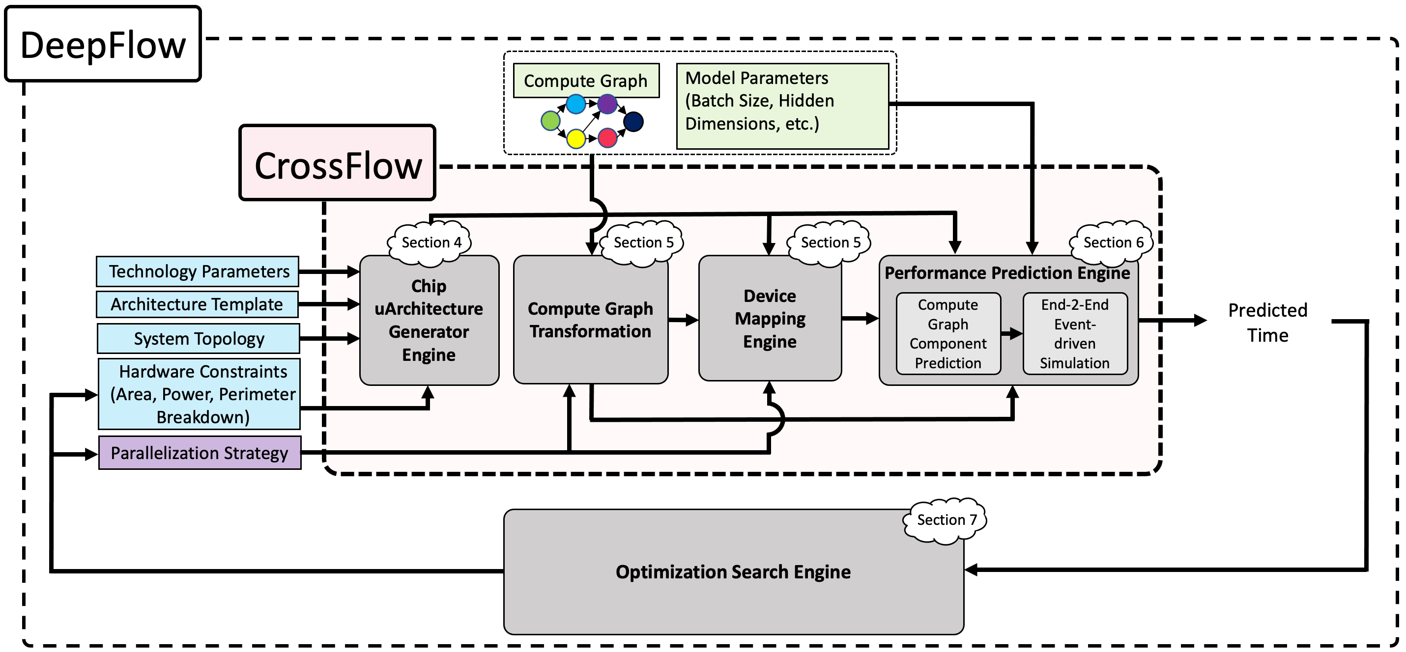
Despite this, the distributed AI training hardware landscape often focuses on just a small set of parallelism strategies for a fixed hardware design [3]. Exploring the trade-offs between parallelization strategy (e.g. data parallelism and model parallelism) and performance (run-time) is often done in an ad-hoc manner. There is no methodical framework or research that explores the trade-offs between low-level hardware technology details and high-level algorithmic design (such as model architecture, parallelism strategy and batch size) on over performance and utilization of compute and memory resources. As a result, we set out to develop a framework that could enable across-the-stack analysis and allow us to look at the optimal points in the vast technology, system and algorithm design space. Towards that goal, we develop CrossFlow, a performance modeling framework that enables “what-if” analysis across different layers of the stack, and DeepFlow that builds on top of CrossFlow and uses machine-learning based techniques to automate the design space search. CrossFlow is an end-to-end performance modeling tool based on an analytical model which takes the entire system-architecture into account and is more sophisticated than a simple Roofline analysis and less time-consuming than simulation. The framework provides a templatized interface for defining technology (minimum operating voltage, bitcell area, etc), chip (compute cores, memory hierarchy, etc.) and system-level architecture (node-level organization, intra-node network, and inter-node network), machine-learning model’s compute graph, and parallelization strategies and predicts run-time per iteration step. Key contributions of this work include:
-
•
We conduct a variety of case studies looking at impact of a variety of high-cost technology innovations on eventual performance of distributed DL training. We show that future logic technology nodes alone would provide minimal performance gains, and advancement in HBM and inter-node network technologies is needed to provide the next leap in performance. Also, optimal parallelism strategy selection could provide more performance gains than using naive parallelism strategies on next generation hardware (Section 9).
-
•
We develop the first open-source, full-stack pathfinding framework, DeepFlow111https://github.com/nanocad-lab/DeepFlow, for large distributed deep learning (DL) training: the driving workload for most future technology, hardware and software development (Section 3- 7).
-
•
We validate CrossFlow performance prediction against measurements on real commercial hardware (NVIDIA P4, V100 and DGX-1) running kernels and DL application in both single and distributed settings, observing near perfect correlation and 10% - 16% error. Next we show that large multi-chip integration and waferscale technologies would not be worthy investments for large scale language models (Section 8).
CrossFlow and DeepFlow can be used to bridge researchers across different layers of the stack (often spanning across different industries) to communicate their needs.
2 Motivation
High-level algorithmic design decisions such as batch size, parallelism strategy and degrees of parallelism stress the underlying hardware components in different ways. One important metric that guides a balanced compute-memory design is computation intensity. Computation intensity is a workload property defined as the ratio of the number of computation flops to number of accesses to main memory.
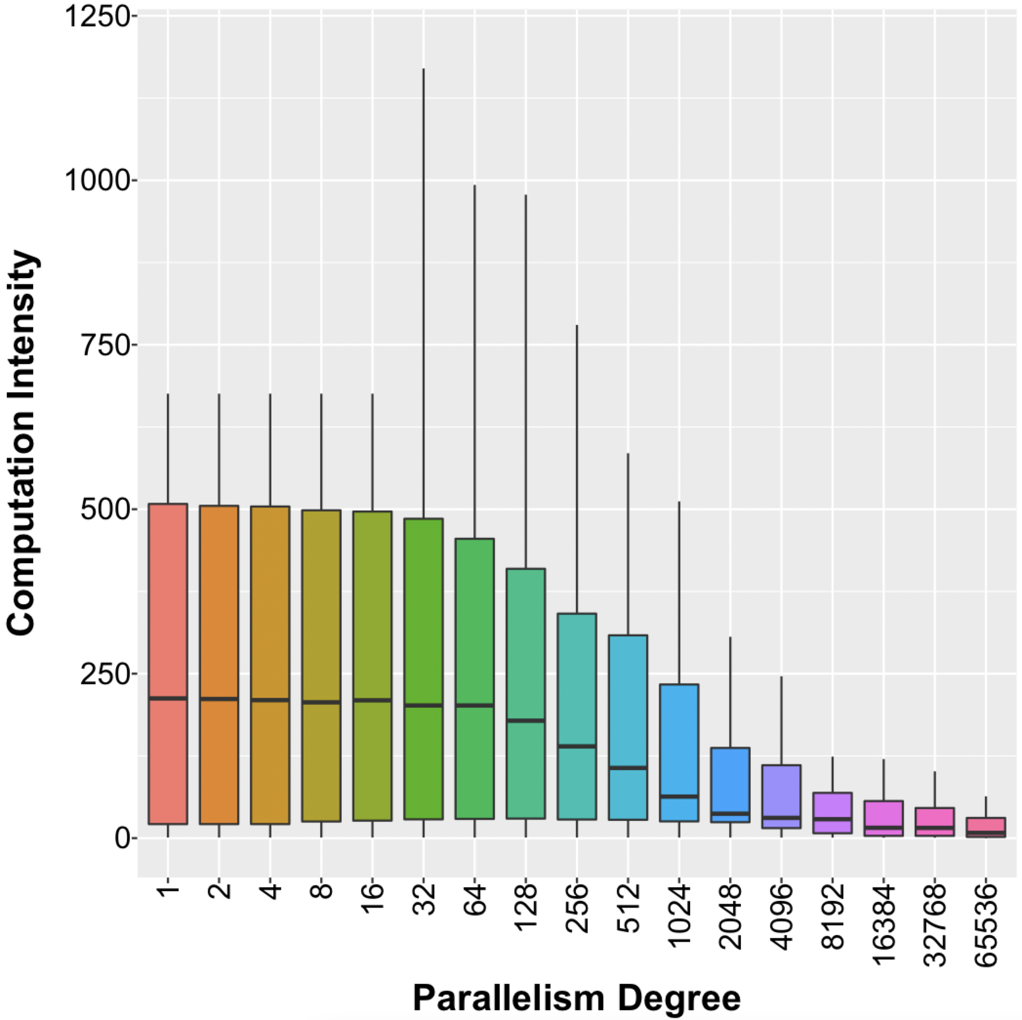
Figure 1 (left) shows the computation intensity distribution across different number of GPUs. We performed this analysis for a GEMM problem of size distributed across many GPUs. Depending on the parallelism strategy and number of available GPUs, each GPU gets a non-regular matrix shards for compute. Each boxplot shows the spread of computation intensity for different number of GPUs. For each level of parallelism, we see a large spread of compute intensities, particularly for lower parallelism degrees. This is the result of different parallelization strategies as well as different tiling strategies. It is clear from this figure that computation intensity is much smaller at higher degrees of parallelism, implying the need for a different design point.
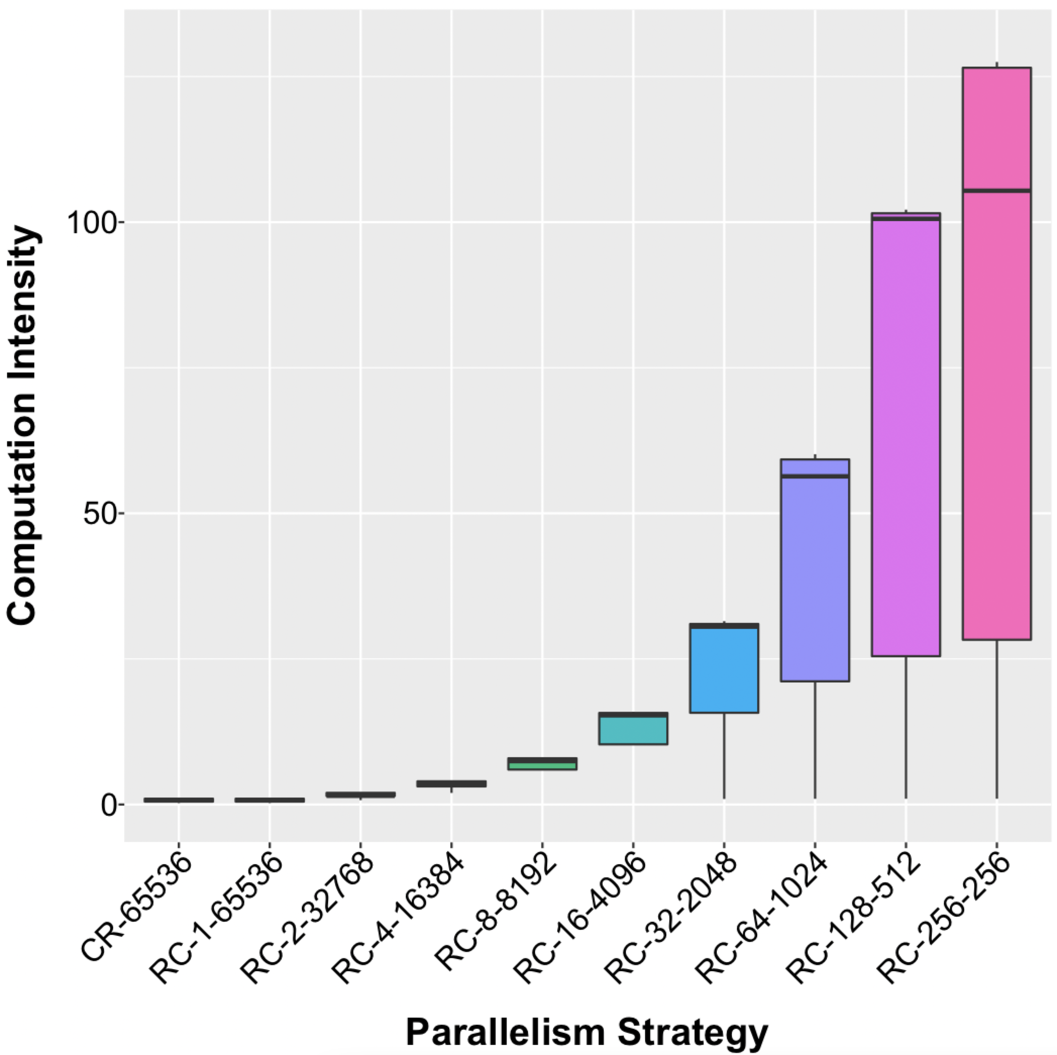
There are a myriad of ways to parallelize a model across a large multi-node system. Figure 1(right) shows the distribution of computation intensity across different parallelization strategies for a fixed level of parallelism (64K GPUs). On the X-axis, we show various parallelization strategies across 64K GPUs. RC or CR refers to Row-Column or Column-Row distributed GEMM (a.k.a kernel parallelism, more details in Section 3.3). As shown, optimal design point is different for different parallelization strategies.
Large training workloads are rapidly becoming the applications driving large investments in semiconductor technology development all the way down to fabrication equipment, making such a cross-layer pathfinding framework immensely valuable to ML engineers, system architects and technology developers alike.
3 DeepFlow Overview
Figure 2 shows an overview of the DeepFlow framework. DeepFlow takes the following set of inputs: (1) System design hierarchy (e.g., the number of accelerator nodes per device, the number of devices in the system, the network topology connecting nodes within a device and across the devices), (2) Architecture template of each accelerator node which provides a high-level definition of its components and how those components fit together. The purpose of the template is to provide a blueprint for the accelerator without committing to any specific hardware parameters. (3) Technology parameters for each hardware component (e.g. energy per flop), (4) Design budgets for each hardware component (area, power, perimeter), (5) Machine learning model specification in the form of a high-level compute graph, parameters of each compute node (kernel type, tensor dimensions), and (6) Parallelism strategy (data, model, kernel, and/or pipeline parallelism dimensions) which distributes the compute graph across the entire system. (7) Device mapping strategy which defines mapping of parallel shards onto hardware nodes. Given these inputs, DeepFlow predicts the end-to-end performance of one iteration (i.e., single batch) of the model and finds an optimal hardware-software-technology design point as output.
DeepFlow is composed of two major components. CrossFlow which operates in a stand-alone mode and can predict performance for any input configuration; and a search and optimization engine (SOE) which enables design space search.
3.1 CrossFlow Building Blocks
Micro-Architecture Generator Engine (AGE)
AGE takes the following set of inputs: (1) Design constraints (i.e the power, area and perimeter budget and breakdown across micro-architectural components such as cache, network, compute cores). This breakdown can be provided manually by users or automatically by the Search and Optimization Engine (SOE, Section 3.2). (2) Technology parameters such as energy per flop, energy per data bit transfer for each level of memory and network hierarchy, threshold and maximum gate voltage, integration substrate parameters such as bump/interconnect pitch. We provide a wide range of standard and future technology libraries as baseline. (3) Architecture template which is a blueprint of the underlying accelerator chip without committing to any specific hardware parameters. Given these input, AGE performs a frequency-voltage-area scaling optimization to generate the following output parameters such that design budgets for all component are met: (1) Compute throughput. (2) Capacity for different levels of memory hierarchy. (3) Bandwidth to each level of memory hierarchy. (4) Inter-node as well as intra-node network bandwidth. These parameters are then utilized by the performance prediction engine (PPE) to estimate the execution time of each kernel.
Compute Graph Transformation and Device Placement Engine (DPE)
The parallelization strategy and device mapping are critical in deciding the overall execution time. Here, we first transform the model graph to a ‘super-graph’ to reflect the parallelization strategy provided by the users manually, or SOE engine (Section 3.2) automatically. For example, to apply data parallelism, the model graph is replicated and appropriate edges are added to model the gradient exchange. After generating the transformed graph, DPE assigns the vertices of the transformed graph to the system nodes following a heuristic approach to minimize the communication overhead.
Performance Prediction Engine (PPE)
We use hierarchical roofline modeling to predict the performance of each compute node. To calculate the overall end-to-end execution time, while respecting scheduling constraints (e.g. one kernel at a time per GPU, or prioritizing one kernel launch over another) we use event-driven simulation.
3.2 Search and Optimization Engine (SOE)
Co-optimizing micro-architectural parameters and the parallelization strategy that minimizes the overall end-to-end execution time requires navigating a large space of design parameters. Search and optimization engine (SOE) enables the automatic design space search and finds an optimal design point which meets the design constraints and minimizes the overall execution time. SOE takes inspiration from ML-assisted search algorithms, in particular gradient decent search with momentum and builds on top of the CrossFlow modeling engine.
3.3 Parallelism Strategy Space
There are a myriad of ways to parallelize a model across a large multi-node system. Exploring the parallelism space and finding the optimal strategy is critical to overall performance and system utilization. DeepFlow explores kernel, data and layer parallelism. It uniquely identifies each parallelism strategy by following notations: RC-{KP1}-{KP2}-d{DP}-p{LP} or CR-{KP1}-d{DP}-p{LP} depending on the choice of kernel parallelism. RC (Row-Column) and CR (Column-Row) refer to different forms of kernel parallelism, i.e. distributed GEMM through inner-product or outer-product implementation. KP1 and KP2 are the parameters of distributed GEMM. For Row-Column (RC) or inner-product, KP1 and KP2 would refer to the number of ways we shard the first matrix across rows and the second matrix across columns. For Column-Row (CR) or outer-product, we would only need one parameter to specify the parallelization strategy; KP1 will refer to the number of ways we cut the first matrix across columns and the second matrix across rows. DP represents the number of model replicas and data shards assigned to each to exploit data parallelism. LP is the number of ways we cut layers into stages to exploit pipeline parallelism.
4 Micro-Architecture Generator Engine
The micro-architecture generator engine, AGE, takes three sets of inputs: (1) A technology components library, where the characteristics of each component such as cores, different types of memories, network interfaces, etc. are defined, (2) Architecture template, where the overall high-level chip and system organization (such as compute and memory hierarchies) is provided, (3) Hardware resource allocation, where area, power, and chip perimeter budgets are provided for the different components of the system. Using this information, the AGE generates the final micro-architecture parameters (such as overall compute throughput, memory bandwidths at different memory levels, network bandwidth) as shown in Figure 2.
4.1 Technology Components Library
A system is generally composed of many primitive components or building blocks such as the compute units, SRAM banks, DRAM, interconnect network components (on-chip and off-chip), etc. A library of these components and their associated technology parameters are provided as input to the tool through a YAML file. We classify these components into three primary categories: compute, memory and network.
4.1.1 Compute
Attributes for the minimal compute components such as matrix-multiplier units, vector-matrix multiply units, or a dataflow architecture unit like systolic array are specified under this category. When a compute component is added to the library, the compute attributes listed in Table I will have to be defined for that component. The tool user can add any type of compute component in the library ranging from a simple scalar unit to a complex unit comprising of a bundle of systolic arrays and capture the micro-architectural characteristics in the final architecture template file.
4.1.2 Memory
The memory components in a system can be built out of different technologies (e.g., SRAM, DRAM, MRAM, RRAM, 3D-XPoint). Also, these memory components can be used in two ways: on-chip memory and off-chip memory. A library of fine-grained memory components can be created and stored under this category which is utilized to construct different levels of the memory hierarchy. The characteristics of the on-chip components are described at the granularity of a bank because the smallest on-chip memory unit available to a system designer is usually a memory bank. The parameters of a memory bank such as capacity, bit area, periphery overhead etc. are taken as inputs. On the other hand, we model the off-chip memory components such as DRAM, or 3D-XPoint at device level granularity, e.g., an HBM stack. This is because the off-chip components are usually obtained at a device level granularity. For off-chip memories, other parameters such as memory controller area, I/O bus width per device, etc. need to be defined. This information is then used to precisely model the capacity and throughput of different levels of the memory hierarchy under the given area and power constraints.
4.1.3 Network
The inter-chip network component is either intra-node or inter-node communication link. In the case of a multi-chip module (MCM) where multiple compute dies and memory devices are integrated on a 2.5D integration substrate within the same package, the inter-die communication is done using high density and energy-efficient links on the 2.5D substrate. These links are considered as intra-node links. On the other hand, the off-package communication links between nodes are considered as inter-node links. The attributes that need to be defined for inter and intra-die communication network components are provided in Table I. In case of a waferscale system, the entire wafer could be considered as a single node.
| Compute | Technology Node | Nominal Area |
|---|---|---|
| Nominal Voltage | Threshold Voltage | |
| Nominal Frequency | Minimum Voltage | |
| Nominal OP rate | Maximum Voltage | |
| On-chip Memory | Technology | Latency |
| Dynamic energy per bit | Static energy per bit | |
| Area per bit and total area overhead | Bank Capacity | |
| Controller area overhead per bank | Controller power overhead per bank | |
| Off-chip Memory | Technology | Number of links per device |
| Dynamic energy per bit | Nominal Voltage | |
| Static power per bit | Nominal Frequency | |
| Device Capacity | Minimum Voltage | |
| Device Area | Maximum Voltage | |
| Memory Controller and I/O Area | Access Latency | |
| Network (intra-node and inter-node) | Nominal Voltage | Number of links per mm |
| Nominal Frequency | Threshold Voltage | |
| Nominal Energy per Link | Minimum Voltage | |
| Nominal Area per Link | Link Latency |
4.2 Architecture Template
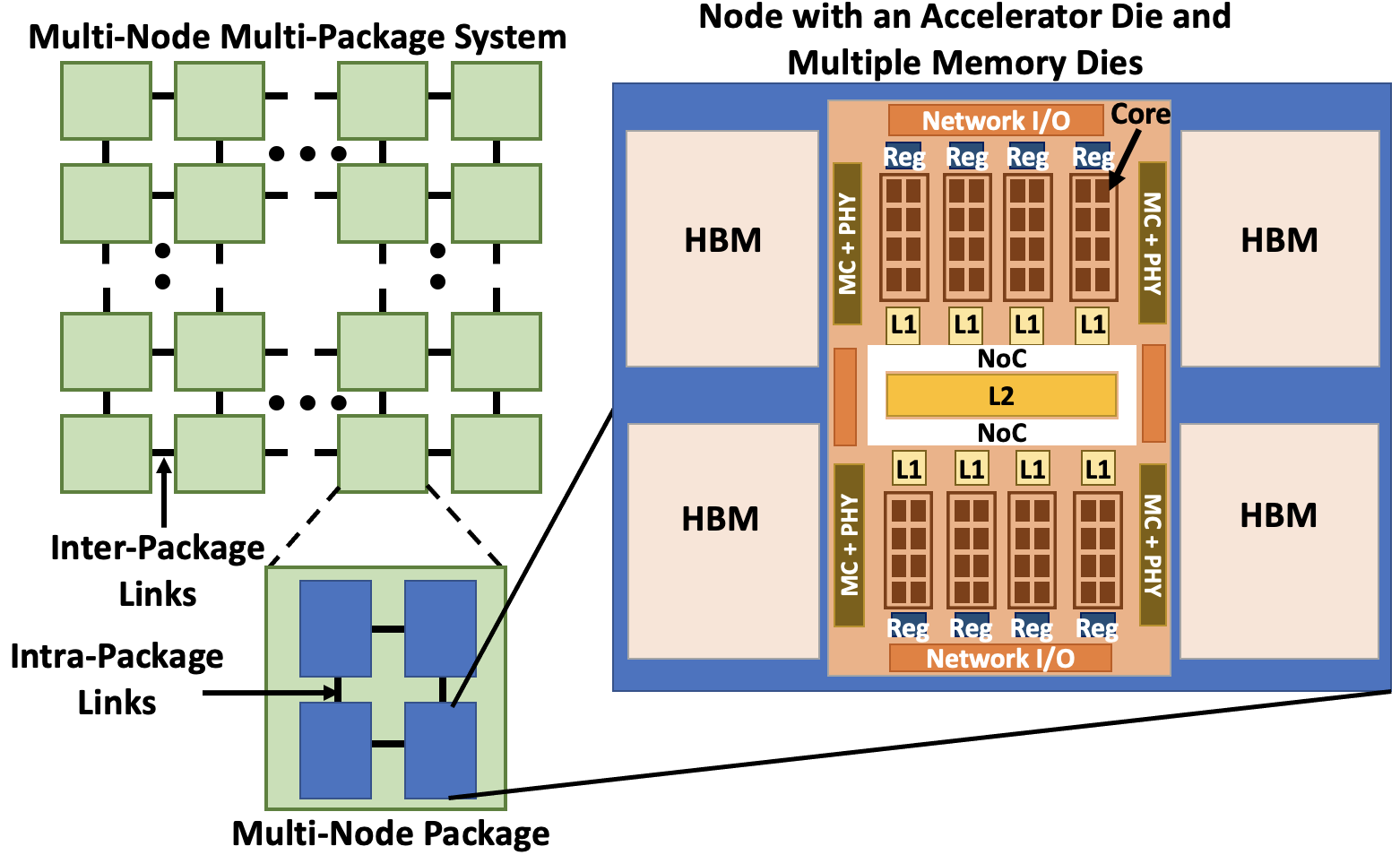
Once all system components are instantiated from the technology library, the next step is to hierarchically organize one or multiple components from each category to construct the overall system. Distributed machine learning training is done on scale-out multi-node system, as shown in Figure 3. Such a system consists of multiple individually packaged nodes which communicate through off-package interconnects (such as NVLink, Infiniband etc.) that form the inter-node network. Inside each package, there can be multiple different accelerator nodes connected using an intra-node network. Each accelerator within the package typically consists of one accelerator die that is connected to its own off-chip main memory components (such as HBM, as shown in the figure). Each accelerator die itself can be composed of smaller compute units.
DeepFlow provides a rich template that can be used to specify the overall architectural organization of such an accelerator system. Next we describe in detail how the template is organized and how different system configurations can be achieved using this template.
4.2.1 Compute unit
As shown in the accelerator die architecture in Figure 3, compute units are often organized in hierarchies. E.g., in an NVIDIA GPU, multiple tensor cores are bundled in a streaming multi-processor (SM) and the SM as a whole interacts with the cache hierarchy. In DeepFlow one can express such hierarchy by defining minimal compute units (MCUs) and MCU bundle. MCU is the smallest compute unit that we expose to the tool user. It defines the dataflow model and layout (e.g. MCU can be a systolic array that its height and width are configurable as input) and interacts with the first level of memory hierarchy. Meanwhile, MCU bundle defines the number of MCUs that are bundled together and are exposed to the second level of memory hierarchy.
In dataflow architectures such as Eyeriss, TPU etc., data can flow directly between different cores. Hence, the tool allows one to define the type of dataflow within an MCU. Currently the performance model supports three types of dataflow: weight stationary, activation stationary and output stationary. The tool can also find the best dataflow strategy among the three for any given kernel.
Software runtime, scheduling overheads and the architecture of the cores often restrict the maximum compute utilization. For example, the tensor-cores in NVIDIA V100 incurs fill-drain related under-utilization during tensor loading from the registers and therefore achieves a maximum utilization of 85%. To account for such overheads, a maximum utilization value can be defined which derates the core throughput by that factor.
4.2.2 Memory Hierarchy and Scope
The memory hierarchy is defined by initializing multiple memory levels from the highest to the lowest level (i.e., registers to the main memory) as shown in Figure 3. Each level of memory has two attributes: (1) Memory technology component from the technology component library which defines the physical attributes of the memory as outlined in Table I, and (2) Scope defines the set of components from the next level of memory hierarchy that are accessible from this level of memory hierarchy. For example, the ‘global’ scope indicates that the memory level is accessible to all the components.
4.2.3 Network Topology
In DeepFlow , we support two levels of network hierarchy: intra-package and inter-package. For each level, a different topology (e.g. mesh, torus, crossbar) can be defined.
4.3 Hardware Resource Allocation
Hardware design under a limited area and power budget is a fine art of finding the right balance (breakdown of resources) across different micro-architectural components. The area and power allocation for each micro-architectural component, as well as the perimeter allocation for certain components derive the design and specification of that component.
We define resource (area, power, perimeter) distribution across different components of the compute chip, as input parameters. The input definition also includes the total area and power budgets for the entire compute node. The total perimeter is inferred from area. The area budget is usually dictated by packaging constraints. For example, if the compute and memory dies are assembled on a 2.5D silicon interposer-based interconnect substrate, the total area of the node will be limited by the maximum size of the interconnect substrate that can be fabricated. Compare this to a waferscale system which houses an entire node on a wafer where the total area budget can be as large as 70,000 . A node’s power budget is determined by the cooling infrastructure that extract heat from the node and the power delivery constraints.
We define budget distribution across different components of the compute graph as a percentage breakdown. As shown in the YAML snippet in Figure 4, fractions of the total area is distributed across cores, levels of memory hierarchy and network components. Similarly, the fraction of the compute chip’s power and perimeter gets devoted to different hardware components.
Given the overall resource allocation and distribution, the AGE performs a series of optimizations (voltage-frequency scaling) to find an optimal parameter settings for each micro-architectural component. An optimal parameter setting is one that utilizes the most of the allocated budget. Note that an unbalanced resource allocation may leave some of the budget under-utilized. While we allow users to provide a manual breakdown of resources as input, we highly recommend to use SOE (Search and Optimization Engine) to automatically find the best setting which maximizes the overall resource utilization.
4.4 Micro-architectural Parameter Generation
Next, the tool generates the micro-architectural parameters for each component of the architecture. Given the architecture template, alongside the resource breakdown across the different components, and the technology parameters, we find the maximum throughput for each component. E.g., We find the maximum number of cores that can fit in the given area allocation and find the voltage-frequency points to maximize compute throughput under the power budget. Similarly, for on-chip caches, we find the memory capacity and memory bandwidth at each level that can fit in the area budget while taking the network and controller overhead into account. For off-chip memories and network interfaces, we use the energy per bit information along with the physical I/O transceiver area, bump pitch as well interconnect wiring pitch to determine the maximum bandwidth that can be realized on the chip (using a model similar to [5]).
These architectural parameters, throughput, bandwidth, capacity etc., are then provided as input to the performance prediction engine. Next, we discuss in detail how we model and calculate these parameters.
4.4.1 Core
For deep learning models, the kernels are usually highly parallel in nature and therefore, our goal is to maximize total compute throughput under the area and power budgets allocated for compute. Given the area budget, we first compute the maximum number of MCUs (minimal compute units, introduced in Section 4.2.1) that can fit within the area allocated. The nominal frequency and voltage for each MCU is an input to the model, therefore the nominal power for each MCU and the entire core can be derived very easily. If the nominal power exceeds the power budget, we scale down the frequency and voltage. If we hit the minimum voltage limit set in the component description, we reduce the number of MCUs till we satisfy the total power budget allocated to the compute units. This explains a case where the core design is power-bound and not area-bound.
Once we determine the total number of cores and the frequency of operation, we compute the compute throughput by appropriately scaling the nominal flop rate, as shown in equation 1.
| (1) |
where is the total number of cores, is the nominal flop rate of each core, is the nominal frequency corresponding to the technology node of the core and is the final optimal operating frequency. We use standard Voltage-Frequency-Power scaling methodology to obtain the operating voltage and frequency.
4.4.2 Register and Cache Memory
The total area and power budgets allocated to each level of on-chip memory is split between the memory banks and the network circuitry that connects the memory banks at each level to micro-architectural components at the next level that are under its scope. We assume this interconnect to have a crossbar topology. The total number of components under its scope and the number of banks in that memory level determine the area and power overheads of the network. We iteratively determine the total number of banks possible at each level of memory hierarchy such that the total area of the banks and the network at every level satisfies the area budget allocation. Once we determine the number of memory banks, we calculate total static power of all the banks (Equation 2) and we allocate the remaining power budget to dynamic access energy. The available dynamic energy budget determines the maximum achievable throughput as shown in Equation 3.
| (2) |
| (3) |
4.4.3 Main Memory
Main memory has two major components that collectively control the overall capacity and bandwidth but are housed in two different places. Memory controller which is placed on the compute chip, and the memory devices are placed outside the compute die within the same package. The area allocation to each component determines the maximum number of memory devices that can be supported, which in turn determines the total memory capacity (see Equation 4).
| (4) |
Meanwhile power and perimeter allocation dictates the number of links (that can fit along the compute die), and the frequency of each link which collectively determine the overall off-chip memory bandwidth.
4.4.4 Network
The off-chip network links (intra and inter-package) consume both power and area on the compute die. Moreover, the wires need to escape the periphery of the die which gets determined by the interconnect density and the available chip perimeter. The maximum number of links that can be accommodated in the compute die is limited either by the area available to fit in the link I/O cells or the amount of perimeter available for the links to escape the die periphery. Therefore, the tool uses the area per link, the available area budget, wiring density and the die perimeter budget to find the maximum number of links that can fit in the chip. Next, the tool uses the standard voltage-frequency scaling methodology to find the operating point for each link such that the total network-related power is within the power budget allocated. The network bandwidth is then calculated by multiplying the total number of links and the operating frequency of each link. We perform this step for the intra-node network and inter-node network separately.
5 Compute Graph Transformation and Device Mapping
Given the ML model description (in form of a compute graph) and the distributed system topology (in form of a system graph), we find an optimal mapping from vertices and edges in the compute graph to hardware nodes and network links in the system graph. However, before mapping, we transform the compute graph into a super-graph to reflect the parallelism strategies specified as input.
5.1 Compute Graph Structure Transformation
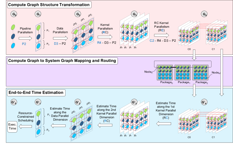
Each parallelism strategy is a form of graph transformation where the sub-graph to be replaced is a single node, so essentially all nodes would be replaced with the same replacement graph. For example, to model data parallelism (with the ring-all-reduce implementation) we would need to replace each node in the original graph with a ring of length (for an -data parallel strategy). The new edges on the ring will be marked as cross-edge to capture the fact that they connect compute nodes hosted on separate devices. To capture a kernel parallelism strategy (e.g. RC-{KP1}-{KP2}), we would need to replace each node in the compute graph with a 2-dimensional torus of dimension (assuming the reduction algorithm along each dimension is ring-all-reduce). Similarly, new edges on the torus would be marked as cross-edge. To capture a pipeline parallelism, no node transformation is required. The pipeline parallelism slices the original graph into multiple sub-graphs, each hosted on a separate hardware node. Edges connecting sub-graphs would be marked as cross-edge. Figure 5 shows the composition of multiple parallelism strategies applied in sequence (pipeline, data and kernel parallelism, respectively). is the original compute graph and is the final transformed graph.
5.2 Device Mapping and Routing Engine
Data parallelism, kernel parallelism and pipeline parallelism would require that each parallel shard to be hosted on a separate physical device. Hence, device mapping happens at the granularity of a parallel shard. We want parallel shards that are close in the parallel space to be mapped onto nodes that are close in the physical space to minimize communication. However, the transformed graph usually has higher dimension than the system graph. Figure 5 shows such example, where the final transformed graph () is 4-D hypercube and the system graph is a 2-D torus. Therefore, it will not be possible to map all adjacent nodes in the compute graph to adjacent nodes in the system graph. We adopt a greedy approach to conduct such mappings: We start with a parallel dimension, map all parallel shards along that dimension to adjacent nodes in the hardware. If the number of shards along the parallel dimension is larger than the hardware dimension we are mapping onto, we wrap-around to the next immediate dimension. We continue this process along other dimensions in a specific order, until all nodes are mapped. The order at which we walk along the parallelism dimensions results in different mappings. For 4 different parallelism strategies, we explore = 24 possible orderings to pick the best mapping. Once node mapping is determined, we take a last step to map edges to physical links. An edge that connects to adjacent node in the compute graph may map to a multi-hop path as shown in Figure 5. As a result, one physical link would be shared across multiple edges. The number of logical edges sharing a physical link is an important factor for effective bandwidth estimation. We use routing to map edges in the compute graph to paths in the system graph. Overall, the whole transformation step followed by device mapping is necessary to find an accurate estimation of edge timing.
6 Performance Prediction Engine
Once mapping is decided for each node and each edge in the transformed graph, performance prediction engine estimates timing for each node and each edge. We then use a resource-constrained scheduling algorithm to find the end-to-end timing.
6.1 Hierarchical Roofline
We use hierarchical roofline analyses [6] to predict the timing of each node in the transformed compute graph. For each node, we estimate the operational intensity (OIL = #flops/#memory accessesL) to each level in the memory hierarchy. We search over the space of possible tiling strategies at each level of memory hierarchy and estimate the number of memory accesses to each level. We explain this in more detail next.
6.2 Memory Hierarchy Modeling
The number of accesses to each level of memory hierarchy is a function of the underlying hardware (memory capacity at each level) and the algorithmic implementation (loop ordering and tiling strategies).
For any given input configuration, we explore random tiling strategies which meet the memory capacity requirement at each level. is the number of tiling strategies at each level and is the number of levels of memory hierarchy. Empirically, we found that for , results in a reasonably accurate estimation.
For a given tiling strategy, it is easy to find the number of times each tile needs to be re-streamed from the next level of memory hierarchy. We start from the lowest level (main memory) and walk upward to estimate the number of accesses. The number of memory accesses at each level is dictated by the tiling strategy at current level and the higher level. For the highest level, the number of accesses is determined by the dataflow strategy exploited at MCU units.
6.3 DataFlow Model
The number of accesses to the highest level of memory hierarchy (i.e. register file) will be determined by the number of instructions executed in the execution engine and the dataflow strategy governing mapping and communication between those engines (e.g. weight stationary, activation stationary and output stationary [7, 8]). The execution engine structure dictates how many times a piece of data could be reused internally before accessing the register file. We refer to this number as reuse factor (K). In a 2-D systolic array with size and , and an input GEMM with size , and at , each data element could be reused or or times, depending on which matrix is stationary. Given the reuse factor, we estimate the number of accesses to register files as follows:
| (5) |
6.4 Inter/Intra-Package Communication Modeling
As discussed in Section 5, compute graph to system graph mapping captures logical edge to physical link mapping. The effective bandwidth for each link is downrated by the number of logical edges sharing the link.
6.5 End-to-End Time Estimation
We use an event-driven simulation to estimate end-to-end timing. Event-driven simulation is basically a resource-constrained critical path analysis. Since multiple compute nodes can map into the same hardware node, event-driven simulation is necessary to avoid resource conflicts and respect resource scheduling constraints (e.g. not more than kernels can run in parallel on each hardware node).
We apply event-driven simulation at the original compute graph where the only parallelism to account for is pipeline parallelism: data parallelism and kernel parallelism would essentially create replicas of the original graph (where the kernel size and/or data size would be different for each node). Given that all replicas by definition are hosted on separate hardware nodes, they can all start and stop at the same time (assuming a homogeneous distribution of data along model replicas and homogeneous distribution of sub-kernels across data replicas) and their timing is deterministic. Hence, there is no need for event-driven simulation at the super-graph granularity.
Figure 5 explain an example of an end-to-end time estimation of a backward pass for a simple 3-layer feed-forward neural network, with 2-level pipeline parallelism (), 3-level data parallelism (), and 8-level kernel parallelism (R4-C2).
7 Design Space Exploration Engine
We denote the set of hardware parameters to explore as , where is the number of micro-architectural components in the hardware accelerator node, and , and capture the percentage of the overall area, power and perimeter allocated to each component, respectively.
Our objective is to find the optimal that minimizes the total run time, , such that , , and . The objective function does not have a closed form, but we can calculate it by querying the performance model (CrossFlow). This problem is an example of a constrained black-box continuous optimization. Since the objective function evaluation (i.e. querying CrossFlow) is considerably cheap (milliseconds), we use a variation of projected gradient descent (GD) optimization to solve for (see 6). Empirically, we found that GD with exponential averaging in the parameter space (rather than gradients) works the best for our problem.
| (6) |
Where and are the input parameters and gradients at time step , is the learning rate and is the discounting factor. We repeat the update steps shown above until convergence or the maximum number of steps (), whichever conditions happens earlier. The final result is very sensitive to initialization. We repeat the steps above from different starting points and return the best result. Empirically, we found that and are sufficient to find a near optimal solution.
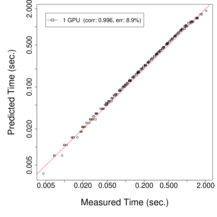
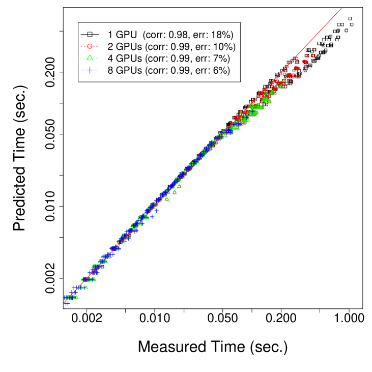
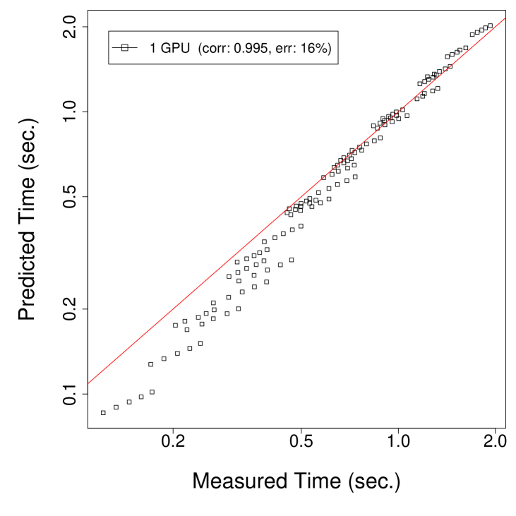
8 Validation
We validate our performance prediction model against execution time measured on real systems (Nvidia P4 with 1 GPU and an NVIDIA DGX-1 system with 8 V100 GPU cards), running distributed GEMM as well as large-scale language models. In particular, we study (2-layer LSTM) language models (LM) for validation and case study as it is deemed to be one of the most challenging applications to scale [9], and is very costly to train [10]. All applications are implemented in Tensorflow 2.0. We use CrossFlow to predict the runtime, which can take anywhere from milliseconds to 20 seconds.
For GEMM validation, we look at a space of more than 2000 GEMM kernels of different shapes and parallelism strategies, where input (m), output (n) and inner dimensions (k) varying from 4K to 32K in steps of 4K, and parallelized across 1, 2, 4, or 8 GPUs, using both Row-Column and Column-Row distributed parallelism strategies. For LM validation, we look into a space of 125 configurations, where Batch Size, Hidden Dimension and Vocab Size varying from 2K to 6K in steps of 1K. We report the correlation (corr), and also the mean relative error (err) to quantify the quality of our predictions.
Figure 8 shows the validation results on Nvidia P4 GPU card. On the X-axis, we show the measured time (in log-scale), and on the Y-axis, we show the predicted time (in log-scale). As shown, predictions and measurements are highly correlated (0.996) and the error is small (8.9%). Figure 8 shows that CrossFlow predictions on a DGX-1 system across 1, 2, 4 and 8 V100 GPU cards are well correlated (0.98-0.99) and have low error (6%-18%). Figure 8 shows the performance of LM on V100 GPU card. Similarly, we can predict performance with high correlation (0.996), and low error (16%). A constant pattern visible across all results is the performance prediction deviation from measurement on real hardware for small kernels. This is expected as Tensorflow 2.0 time measurement hooks include all the software stack latency; while this overhead is negligible for large kernels, it accounts for a large portion of total run-time if the kernel is very small. This indicates the tool outcome would be more reliable for large kernels and large models.
9 Case Studies
DeepFlow is a pathfinding framework with studies and use cases spanning semiconductor technology development, micro-architecture, neural network models, and algorithmic parallelization techniques. In this section, we give few example case studies for a large-scale language model (hidden dim: 16K, global batch size: 16K, vocab size: 800K, number of layers: 2, sequence length: 20) distributed across 512 hardware nodes. For future technology exploration, we study 7 consecutive logic technology nodes (from 12nm (N12) to 1nm (N1). Based on the recent scaling trends for logic technologies [11, 12], we assume area and power scale by 1.8 and 1.3 from one node to the next for iso-performance), 4 different memory technologies (HBM2 (1 TB/s), HBM2e (2 TB/s), HBM3 (projected 2.6 TB/s [13]), and HBM4 (projected 3.3 TB/s)) and 3 different network technologies (Infiniband-NDR-x8 (100 GB/s), XDR-x8 (200GB/s) and GDR-x8 (3.3 TB/s)). The caveat to these results (as with any pathfinding study with DeepFlow) is that if the system architecture or dataflow or neural network is radically different (e.g., this study assumes that same node is homogeneously replicated within the package), the conclusions may change.
9.1 Impact of Technology Scaling
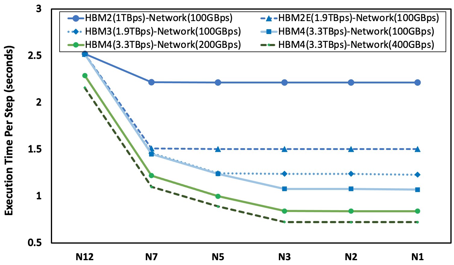
The first question we seek to answer is where the performance bottlenecks are across the stack and which technology could provide the maximum end-to-end performance benefit? Semiconductor technology development decisions are increasingly driven by machine learning as the workload. Many of these decisions trigger large, multi-year investments. Figure 9 shows the impact of scaling logic, memory, and network technology for a large-scale language model using data-parallelism. For these experiments, we assume that power/node = 300W and area/chip = 850 .
Logic scaling improves compute throughput, and also caching capacity and bandwidth, but only to a smaller extent. Going from N12 to N7, we observe a jump in performance irrespective of memory technology. This is because at N12, the performance of a significant number of kernels are L2 bandwidth bound. At N7, the L2 bandwidth and capacity improve enough for HBM bandwidth to become the new bottleneck. Therefore, with improvement in HBM bandwidth, the balance can shift back again to caches and saturation point can be further improved with logic scaling, hence saturation point shifts further to the right. This trend continues up to N3. Beyond N3, even at very high memory bandwidth (3.3 TB/s) and network bandwidth (400 GB/s) performance stays unchanged as cache capacity and bandwidth are the main bottlenecks. Since the on-chip network connecting MCUs to cache and the cache controller overhead scale along with number of cache banks and the number of MCUs (which scale at per technology node), the cache capacity as well as bandwidth increase only marginally at N2 and N1. These trends are well inline with commercial examples from NVIDIA and AMD, where jump to N7 node provided large performance benefits and then, multiple high-end SKUs of the GPUs with higher bandwidth HBM memories have been released for further performance improvements.
Network technology scaling is another big factor that determines overall end-to-end performance of a distributed deep learning system. As logic and memory technologies scale alongside the size of the models, more inter-node bandwidth is needed to accelerate the inter-node communication collectives. Our analysis (Figure 9) shows that beyond N3, scaling networking technology will provide much larger performance gains as opposed to logic scaling. This trend also aligns with the recent efforts in the industry to push high bandwidth and low energy networking technologies and architectures for inter-node and intra-node communication, targeted towards deep learning systems [14, 15, 16].
9.2 Co-optimizing Technology, Parallelism Strategy and Hardware Architecture Design
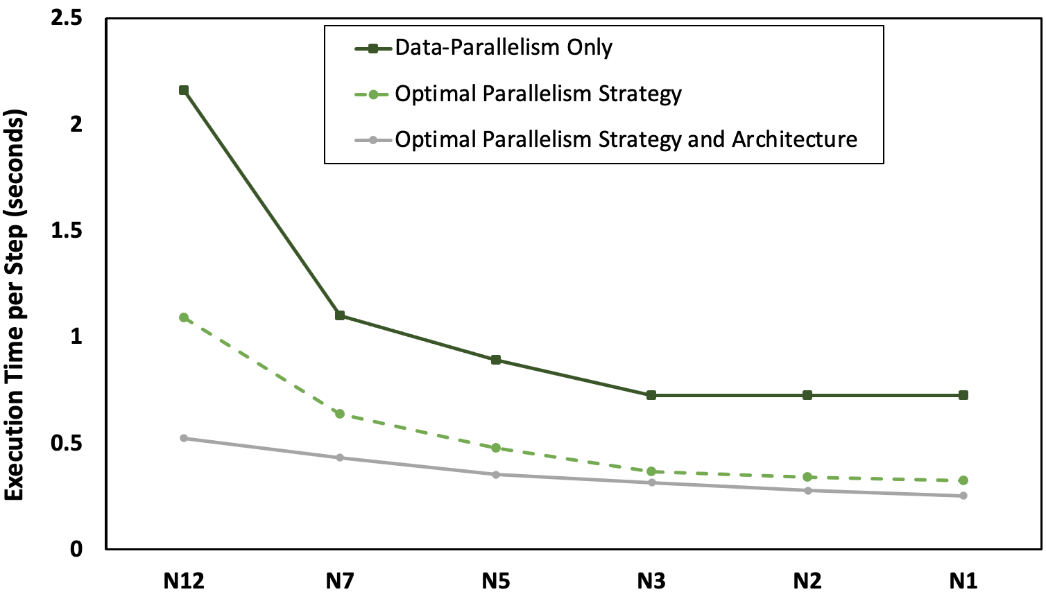
Figure 10 shows the importance of co-optimizing technology with parallelism and hardware design in an incremental fashion. As shown: (1) Parallelism strategy optimization alone can offer performance improvement. (2) Co-optimizing architecture and parallelism strategy offers meaningful benefits for mature technology (12nm and 7nm) nodes. But for more advanced technology nodes, only marginal benefits (20%-30%) can be gained on top of parallelism strategy optimization. (3) For current and near-future technology nodes, co-optimizing for model architecture can provide as much benefit as scaling technology nodes (by almost two generations).
9.3 Effect of Multi-Node Package
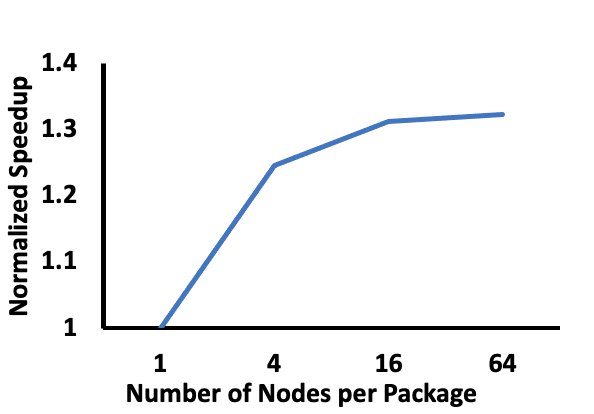
Next, we evaluate the performance improvement that multi-node packaged systems (e.g., MCM-GPU [17], waferscale-GPU [18], Tesla Dojo [19]) can provide in a distributed training setup (see Fig. 11). We assumed 2TB/s link bandwidth for the intra-package links and performed both parallelism and architecture search for each case.
Couple of key takeaways from these experiments were: (1) Increasing the number of nodes in a package improves overall performance by roughly 32% at best. (2) Beyond 4-nodes per package, performance improvement is marginal. Since ultra-large packages or waferscale integration dramatically worsens cost, we believe that such technologies may not be worthy investments for scaling large language model training. These conclusions hold across multiple different batch sizes, hidden dimension sizes and intra-node link bandwidths.
10 Related Work
Related work can be broadly categorized into (1) performance modeling frameworks for spatial architectures like TimeLoop and Maestro, (2) performance modeling frameworks for parallelism exploration such as FlexFlow, and (3) what-if analysis tools like DayDream and Habitat.
Similar to TimeLoop [8] and Maestro [20], we use an analytical model to estimate performance, however, the scope of DeepFlow is much broader. TimeLoop and Maestro model a single kernel runtime on the spatial architecture like systolic array or Eyeriss. Similarly, Mind Mapping [21] is a gradient based search tool that finds the best tiling and mapping strategy for a single compute unit and is built on top of Timeloop. In this regard, all these prior work are similar to analytical models that goes into DeepFlow’s MCU modeling. However, DeepFlow offers more than MCU modeling. DeepFlow allows to capture not only the behavior of an MCU unit but also an entire GPU (through modeling of communication across MCU units through shared layers of memory hierarchy) as well as modeling a data center full of GPUs. Besides, prior work validates against simulators on micro-kernels. We validate our model against SOTA GPU hardware on real-world applications. Furthermore, DeepFlow models an entire compute graph, composed of many kernels mapped and distributed across multiple GPU nodes, and allows the analysis of parallelism at this level, including pipeline, data and kernel parallelism. Moreover, DeepFlow provides four degrees of freedom to explore: model architecture, hardware architecture, technology configuration and parallelism strategy.
FlexFlow [22] is an ML-based model for exploring the best parallelism strategy which relies on the runtime profiling tools to measure kernel timings on the target hardware. While it provides a very rich input for expressing different model architectures, it can only model existing hardware, hence not suitable for parallelism-architecture-technology co-design exploration.
DayDream [23] is a what-if analysis tool that enables researchers to evaluate the efficacy of different algorithmic optimizations for an existing hardware. However, it relies on fine-grain profiling tools to construct dependency graph, hence it lacks the ability to predict individual kernel run-time on non-existing hardware and cannot be used for architecture or technology co-design space exploration. Similarly, Habitat [24] predicts deep learning workloads’ run-time across different existing GPUs, using a combination of wave scaling and MLP predictors. Wave-scaling can only model simple uarchitectural modification, and MLP predictors are u-architecture specific models that require collecting a large set of runtime data on the baseline and target hardware for model training, hence cannot be applied to non-existing hardware.
Astra-sim [25] is a simulator for hardware-software co-design of distributed deep learning systems. The focus of the paper is on detailed modelling of the inter-node network and they study the effects of network topologies and architecture choices. Astra-sim doesn’t explore automated technology and architecture exploration and may not be suited for across the stack design space exploration because of the detailed and heavy-weight focus on network effects.
11 Conclusion
We proposed DeepFlow, a performance modeling framework that enables a cross-stack analysis for hardware-software-technology co-design at-scale. We envision DeepFlow to be used by ML practitioners (to decide what hardware to use to maximize their utilization, or simply predict their hypothetical model architecture performance which might not be realizable in today’s hardware for many reasons including capacity limitation), by system designers (to decide what hardware accelerators they need to acquire or build from scratch to meet their application needs, what new technologies to invest in, etc.), and finally by technology experts (to guide future technology development by assessing its impact all the way across the stack, at scale). Our future work plans to extend DeepFlow modeling to other applications beyond language models and GEMM kernels.
References
- [1] OpenAI, “AI and Compute.” https://openai.com/blog/ai-and-compute/.
- [2] K. Olukotun, “Accelerating software 2.0,” ScaledML, 2020.
- [3] Z. Jia, M. Zaharia, and A. Aiken, “Beyond data and model parallelism for deep neural networks,” arXiv preprint arXiv:1807.05358, 2018.
- [4] A. A. Inferentia, “Achieve 12x higher throughput and lowest latency for PyTorch Natural Language Processing applications out-of-the-box on AWS Inferentia.” https://tinyurl.com/3mbuetmr, (accessed Sep 10, 2021).
- [5] S. Pal and P. Gupta, “Pathfinding for 2.5D Interconnect Technologies,” in System-Level Interconnect - Problems and Pathfinding Workshop, SLIP ’20, (New York, NY, USA), ACM, November 2020.
- [6] S. Williams, A. Waterman, and D. Patterson, “Roofline: An insightful visual performance model for multicore architectures,” Commun. ACM, vol. 52, p. 65–76, Apr. 2009.
- [7] Y.-H. Chen, T. Krishna, J. S. Emer, and V. Sze, “Eyeriss: An energy-efficient reconfigurable accelerator for deep convolutional neural networks,” IEEE Journal of Solid-State Circuits, vol. 52, no. 1, pp. 127–138, 2017.
- [8] A. Parashar, P. Raina, Y. S. Shao, Y.-H. Chen, V. A. Ying, A. Mukkara, R. Venkatesan, B. Khailany, S. W. Keckler, and J. Emer, “Timeloop: A systematic approach to dnn accelerator evaluation,” in 2019 IEEE International Symposium on Performance Analysis of Systems and Software (ISPASS), pp. 304–315, 2019.
- [9] J. Hestness, N. Ardalani, and G. Diamos, “Beyond human-level accuracy: Computational challenges in deep learning,” in Proceedings of the 24th Symposium on Principles and Practice of Parallel Programming, pp. 1–14, 2019.
- [10] “Deep Learning’s Diminishing Returns.” https://spectrum.ieee.org/deep-learning-computational-cost. Accessed: 2021-10-15.
- [11] A. Stillmaker and B. Baas, “Scaling equations for the accurate prediction of CMOS device performance from 180nm to 7nm,” Integration, vol. 58, pp. 74–81, 2017.
-
[12]
“Wikichip: Technology Node.”
https://en.wikichip.org/wiki/
technology_node. Accessed: 2021-10-15. - [13] “HBM3: Big Impact On Chip Design.” https://semiengineering.com/hbm3s-impact-on-chip-design/. Accessed: 2021-10-15.
- [14] L. Poutievski, O. Mashayekhi, J. Ong, A. Singh, M. Tariq, R. Wang, J. Zhang, V. Beauregard, P. Conner, S. Gribble, R. Kapoor, S. Kratzer, N. Li, H. Liu, K. Nagaraj, J. Ornstein, S. Sawhney, R. Urata, L. Vicisano, K. Yasumura, S. Zhang, J. Zhou, and A. Vahdat, “Jupiter evolving: Transforming google’s datacenter network via optical circuit switches and software-defined networking,” in Proceedings of the ACM SIGCOMM 2022 Conference, SIGCOMM ’22, (New York, NY, USA), p. 66–85, Association for Computing Machinery, 2022.
- [15] R. Urata, H. Liu, K. Yasumura, E. Mao, J. Berger, X. Zhou, C. Lam, R. Bannon, D. Hutchinson, D. Nelson, L. Poutievski, A. Singh, J. Ong, and A. Vahdat, “Mission apollo: Landing optical circuit switching at datacenter scale,” 2022.
- [16] NVIDIA, “NVLink and NVSwitch.” https://www.nvidia.com/en-us/data-center/nvlink/, 2022.
- [17] A. Arunkumar, E. Bolotin, B. Cho, U. Milic, E. Ebrahimi, O. Villa, A. Jaleel, C.-J. Wu, and D. Nellans, “Mcm-gpu: Multi-chip-module gpus for continued performance scalability,” in 2017 ACM/IEEE 44th Annual International Symposium on Computer Architecture (ISCA), pp. 320–332, 2017.
- [18] S. Pal, D. Petrisko, M. Tomei, P. Gupta, S. S. Iyer, and R. Kumar, “Architecting waferscale processors - a gpu case study,” in 2019 IEEE International Symposium on High Performance Computer Architecture (HPCA), pp. 250–263, 2019.
- [19] “Tesla Dojo.” https://www.nextplatform.com/2022/08/23/inside-teslas-innovative-and-homegrown-dojo-ai-supercomputer/. Accessed: 2022-10-15.
- [20] H. Kwon, P. Chatarasi, V. Sarkar, T. Krishna, M. Pellauer, and A. Parashar, “Maestro: A data-centric approach to understand reuse, performance, and hardware cost of dnn mappings,” IEEE Micro, vol. 40, no. 3, pp. 20–29, 2020.
- [21] K. Hegde, P.-A. Tsai, S. Huang, V. Chandra, A. Parashar, and C. W. Fletcher, “Mind mappings: Enabling efficient algorithm-accelerator mapping space search,” in Proceedings of the 26th ACM International Conference on Architectural Support for Programming Languages and Operating Systems, ASPLOS 2021, (New York, NY, USA), p. 943–958, Association for Computing Machinery, 2021.
- [22] W. Lu, G. Yan, J. Li, S. Gong, Y. Han, and X. Li, “Flexflow: A flexible dataflow accelerator architecture for convolutional neural networks,” in 2017 IEEE International Symposium on High Performance Computer Architecture (HPCA), pp. 553–564, 2017.
- [23] H. Zhu, A. Phanishayee, and G. Pekhimenko, “Daydream: Accurately estimating the efficacy of optimizations for DNN training,” in 2020 USENIX Annual Technical Conference (USENIX ATC 20), pp. 337–352, 2020.
- [24] X. Y. Geoffrey, Y. Gao, P. Golikov, and G. Pekhimenko, “Habitat: A Runtime-Based computational performance predictor for deep neural network training,” in 2021 USENIX Annual Technical Conference (USENIX ATC 21), pp. 503–521, 2021.
- [25] S. Rashidi, S. Sridharan, S. Srinivasan, and T. Krishna, “Astra-sim: Enabling sw/hw co-design exploration for distributed dl training platforms,” in 2020 IEEE International Symposium on Performance Analysis of Systems and Software (ISPASS), pp. 81–92, 2020.