Two-dimensional spin systems in PECVD-grown diamond with tunable density and long coherence for enhanced quantum sensing and simulation
Abstract
Systems of spins engineered with tunable density and reduced dimensionality enable a number of advancements in quantum sensing and simulation. Defects in diamond, such as nitrogen-vacancy (NV) centers and substitutional nitrogen (P1 centers), are particularly promising solid-state platforms to explore. However, the ability to controllably create coherent, two-dimensional spin systems and characterize their properties, such as density, depth confinement, and coherence is an outstanding materials challenge. We present a refined approach to engineer dense ( 1 ppmnm), 2D nitrogen and NV layers in diamond using delta-doping during plasma-enhanced chemical vapor deposition (PECVD) epitaxial growth. We employ both traditional materials techniques, e.g., secondary ion mass spectrometry (SIMS), alongside NV spin decoherence-based measurements to characterize the density and dimensionality of the P1 and NV layers. We find P1 densities of 5-10 ppmnm, NV densities between 1 and 3.5 ppmnm tuned via electron irradiation dosage, and depth confinement of the spin layer down to 1.6 nm. We also observe high (up to 0.74) ratios of NV to P1 centers and reproducibly long NV coherence times, dominated by dipolar interactions with the engineered P1 and NV spin baths.
Solid-state spins constitute a powerful platform for quantum technologies. They can exhibit long quantum coherence, even up to room temperature, are naturally trapped, making them robust and easy to use, and can be simply integrated with sensing targets at nanoscale distances, making them advantageous for quantum sensing.Degen et al. (2017); Schirhagl et al. (2014); Rondin et al. (2014); Casola et al. (2018) Further, dense ensembles of coherent spins provide a starting point for investigating strongly interacting spin systemsRovny et al. (2018); Cappellaro and Lukin (2009); Yao et al. (2014); Choi et al. (2017, 2020); an S. A. Dzuba and Raitsimring (1981) in which novel, many-body states can arise with applications in both quantum simulation and sensing.
Two dimensional confinement of dense, coherent spin ensembles opens up a number of experimental avenues. Dimensionality plays a critical role in the nature of many-body states, with reduced dimensionality giving access to unique phases and phenomena such as interaction-driven localization.Yao et al. (2014, 2018); Chomaz et al. (2019); Burin (2015); Abanin et al. (2019) Furthermore, because the 3D angular average of the dipole-dipole interaction yields zero, reduced dimensionality is necessary for collective phenomena such as dipolar-driven spin squeezingPerlin et al. (2020) and plays an important role in the decoherence dynamics of many-body systems.Davis et al. (2021)
For sensing applications, a dense 2D layer of sensors in close proximity to a sensing target exhibits enhanced spatial resolution (set by the depth of the layer) compared to a 3D ensemble at the same volumetric density, while benefiting from either classical sensitivity enhancements or entanglement-driven enhancements. Lastly, dense 2D ensembles could serve as a starting point for targeted, on demand formation of individual, optically resolvable defects at specific locations, such as inside nanostructures. Altogether, creating thin spin layers with tunable density is of intense current interest but has been minimally explored in solid-state electronic spin systems to date.
In this paper, we explore defects in diamond, an ideal host for solid-state spin qubits. Diamond’s wide bandgap of 5.4 eV, high Debye temperature of 2250 K, and predominantly nuclear spin-free 12C composition (when grown synthetically using isotopic engineering) provide an exceptionally quiet lattice environment for a myriad of embedded defects with long quantum coherence. The most well-explored qubit system in diamond is the negatively charged nitrogen-vacancy (NV) defect, whose spin can be easily manipulated and read out at room temperature using optical and microwave radiation and has been leveraged for a number of notable experiments in quantum sensing.Degen et al. (2017); Schirhagl et al. (2014); Casola et al. (2018) Substitutional nitrogen, known as the P1 center, is another diamond defect that may be used for quantum simulationDavis et al. (2021) or building multi-qubit quantum registers Degen et al. (2021) when used in conjunction with the optically addressable NV center. While much of the diamond qubit literature focuses on single NV spins for high spatial resolution quantum sensing, dense ensembles of defects (either NV or P1) are becoming increasingly important for a number of experiments leveraging interacting many-body systems.Zhou et al. (2020); Davis et al. (2021) The engineering and characterization of such systems will be the focus of this work.
The creation of tunably dense, coherent, two-dimensional spin layers in diamond is challenging. Ion implantation, the most commonly used method for forming depth-confined defects, suffers from two challenges. First, the high energy of the implanted ions results in decoherence-producing collateral damage (e.g., vacancy-related defects),Tetienne et al. (2018) which is exacerbated for the large implantation dosages necessary to achieve high spin densities. Second, implantation results in a broadened depth distribution of the implanted element. Thin layer confinement can be improved with lower energy implantation, but the spread of depths of these shallowly implanted defects has been observed to be greater than that predicted by SRIM simulations. Kawai et al. (2019); Bluvstein et al. (2019a) More fundamentally, defect properties degrade significantly near the surface,Myers et al. (2014) which is particularly undesirable for quantum simulation where spin-spin interactions must dominate over external decoherence sources. Overgrowth after shallow implantation is a path towards improved coherence but risks passivation and loss of defects during the growth.Findler et al. (2020)
An alternative pathway toward engineering dense, thin spin layers is delta-doping during plasma-enhanced chemical vapor deposition (PECVD) diamond growth. This technique, pioneered by Ohno et al.Ohno et al. (2012) for low density ( ppmnm) layers and further employed by others,Bogdanov et al. (2021); Jaffe et al. (2020); Lobaev et al. (2017, 2018); McLellan et al. (2016) allows for control over the dopant thickness and density in a gentle, bottom-up approach that can preserve long coherence. Vacancy-related defects can be subsequently promoted via a variety of irradiation methods for further tunability of defect density and location. To date, the growth and irradiation approach has predominantly focused on creation of 3D ensembles, Eichhorn et al. (2019); Farfurnik et al. (2017) with only a few studies investigating dense ( 1 ppmnm), thin defect layers where spin-spin interactions may become relevant. Bogdanov et al. (2021, 2019); Davis et al. (2021)
In this work, we create highly confined two-dimensional nitrogen layers in diamond via delta-doping during PECVD growth. Benefiting from an increased understanding of nitrogen incorporation, we identify a set of growth parameters that yields depth confinement of the doped nitrogen layer down to 1.6 nm, as measured by secondary ion mass spectrometry (SIMS). We further confirm the 2D nature of the nitrogen spins via spin-based sensing methods, specifically via the decoherence profile of colocalized NV center probe qubits, which are formed via 200 keV electron irradiation and annealing. We next use several methods to quantify the P1 and NV densities and discuss their relative merits. From the timescale of the NV qubit decoherence, we measure the P1 density to be 5-10 ppmnm. This density measurement is notably 6-8 times smaller than the nitrogen density extracted by SIMS, and we put forth reasoning in support of the accuracy of the qubit-based measurements. To estimate the NV density, we introduce a new, simple Rabi contrast-based method and benchmark it against other qubit-based density estimation techniques. With the Rabi-assisted fluorescence method, we measure an NV density of 1-3.5 ppmnm, tuned via electron irradiation dosage. We find a high NV/P1 ratio of up to 0.74 and propose a model to support the increased conversion for a 2D nitrogen layer. Importantly, the NV centers show reproducibly long coherence times, both for ensembles and single NVs, and we find that the coherence is predominantly limited by spin-spin interactions within the dense P1 and NV bath. Altogether, this work presents a joint materials and qubit-based approach to engineer and characterize interesting spin systems for applications in quantum technologies.
I Material growth, characterization, and preparation
PECVD diamond growth and nitrogen delta-doping
Creating nanometer-scale layers and interfaces via in-situ doping during PECVD diamond growth is typically difficult with fast growth rates, on the order of a few m/hr, and the residual times of the dopant gas.Achard et al. (2020) Here we adopt a slow growth approach that allows for precise depth control and promotes high epitaxial quality of the diamond film. Through use of a low power (750 W, 25 Torr) plasma, low methane concentration (0.1% of the 400 sccm H2 flow), and sample holder temperature of 750° C as measured via a pyrometer, we achieve a slow epitaxial growth rate of 10-30 nm/hr. The diamond epilayers are grown on (100) oriented electronic grade diamond substrates (Element Six Ltd.). Prior to growth, substrates are fine-polished by Syntek Ltd. to a surface roughness of 200-300 pm and also undergo a 4-5 m etch to relieve polishing-induced strain.
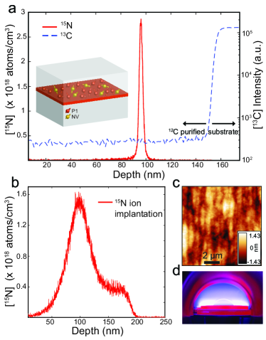
During the nitrogen delta-doping period of growth, all plasma conditions are held constant, and 15N2 gas (1.25% of the total gas content) is introduced into the chamber briefly to create a delta-doped layer. Optical emission spectroscopy (OES) is used to record the residual time of nitrogen in the chamber following doping, which is found to be just 22 seconds. The 15N2 doping time in this work is set to be 15 minutes; however, the delta-layer thickness is less than expected given the pre-doping growth rate. This observation contrasts the assertion that nitrogen doping enhances growth ratesde Theije et al. (2000) and suggests that during the delta-doping phase the plasma chemistry changes significantly such that steady growth is slowed or interrupted. Further investigation is needed to better understand the growth rate discontinuity that allows for thin layer creation and will be the subject of future work. The 15N isotope is used to spectroscopically distinguish doped P1 and NV centers from the 99.6% natural abundance 14N isotope in the substrate, via the differences in hyperfine coupling to the N nuclear spin. We use isotopically purified methane (99.999% 12CH4, Cambridge Isotope Laboratories) to engineer a diamond lattice environment composed of 99.998% 12C, as measured by SIMS (Fig. 1a), thus largely removing 13C, an isotope with nonzero nuclear spin that contributes magnetic noise and induces NV center decoherence.
A number of parameters are known to affect the density of nitrogen incorporated during growth, including the growth temperature,Tallaire et al. (2015) gas flow ratios,Lobaev et al. (2018) and misorientation angle of the seed substrate.Meynell et al. (2020); Lobaev et al. (2018) We find that the epitaxial growth rate, which encompasses the effect of all of these parameters, displays the most clear relationship to nitrogen incorporation. To control the growth rate, and hence nitrogen incorporation, we modify the miscut angle of the substrate following recent work,Meynell et al. (2020) while keeping temperature and gas flow rates constant. We specify the miscut angle by first measuring the virgin substrates using x-ray diffractometry (XRD) rocking curve measurements about the (004) omega peak and subsequently using off-angle fine polishing (Syntek Ltd.) to target a 1.0-1.5° miscut. In this miscut range, we observe increased nitrogen incorporation with increased growth rate.
After growth, the diamonds are further electron irradiated and annealed to generate enhanced NV center concentrations. Irradiation is performed with the 200 keV electrons of a transmission electron microscope (TEM, ThermoFisher Talos F200X G2 TEM). This energy is just above the carbon atom displacement threshold energy of 145 keV for (100) diamond,McLellan et al. (2016); Koike et al. (1992) thus allowing us to target the formation of single vacancies and minimize extended lattice damage which may occur with higher energies.Campbell and Mainwood (2000) The irradiation time is varied to create spots that range in dose from - e-/cm2. The samples then undergo subsequent annealing at C for 6 hours in an Ar/H2 atmosphere, during which the vacancies diffuse and form NV centers. After irradiation and annealing, the samples are cleaned in a boiling piranha solution (3:1 H2SO4:H2O2) to remove surface contaminants and help stabilize the negative NV- charge state for further measurements. All data in the main text of this paper were taken on one sample (sample A). To demonstrate repeatability of our growth, preparation, and characterization techniques, we present data on a second, similarly prepared sample (sample B) in the supplemental information (SI).
Secondary ion mass spectrometry analysis
The primary bulk materials characterization tool for depth-resolved elemental analysis is SIMS, in which a primary ion beam is directed at a sample, sputtering away material and collecting information about the elemental and isotopic composition as a function of depth. We use a CAMECA IMS 7f dynamic SIMS instrument with a primary Cs+ beam energy of 7 kV, and current of 30 nA at an incident angle of to achieve a sputtering rate of approximately . The sample is biased to -3000 V and 12C15N- negative secondary ions are detected using a high mass resolving power, M/M = 6006. Only ions from the central are collected from the sputtering crater to avoid edge effects. We observe a delta-doped layer of thickness 3.55(0.04) nm, as determined from the full width at half-maximum (FWHM) of the peak in the nitrogen depth profile illustrated in Fig. 1a. The error represents a 95% confidence interval for a Gaussian peak fit. Importantly, the thickness of this layer is significantly narrower than for a sample in which nitrogen was introduced via a standard implantation technique targeting a similar depth, as can be seen in Fig. 1b. This sample was implanted with 15N ions at 90 keV, 1 dose e-/cm2, and a 7 tilt to mitigate ion channeling. However, channeling is still observed in the SIMS data, as evidenced by the peak’s shoulder extending out to 200 nm depth. The FWHM of the main peak at 100 nm depth fit with a Gaussian is 53.3(0.2) nm, which is significantly broader than the delta-doped layer, and furthermore broadened compared to the expected 42.2 nm FWHM predicted by SRIM simulation.Ziegler et al. (2010)
SIMS depth resolution is limited by the sample’s surface roughness which causes ion mixing at the doped layer interface, and thus the thickness of sample A is convolved with its surface roughness (Fig. 1c.) and may represent an upper bound. However, under similar SIMS measurement parameters we have observed an even thinner layer of 1.61(0.02) nm thickness in a different sample grown with a shorter, five-minute doping time (SI Fig. S1a). This observation suggests that the SIMS resolution may not be the dominant limitation in our measurement, but without a secondary characterization, the exact layer thickness remains unknown.
From the SIMS data we can also extract a quantitative estimate of the dopant density by comparing the signal strength to a reference standard with a known dopant dose introduced by ion implantation and calculating a relative sensitivity factor (RSF). Taking the background 12C matrix into account and assuming similar instrumental conditions between runs, the RSF can be used to determine the atomic concentrations of the doped nitrogen. Further details on the RSF calibration are given in the SI. We integrate over three standard deviations of a Gaussian-fit peak shown in Fig. 1a, to calculate an areal density of 1.057(0.009) atoms/cm2 or 60.1(0.5) ppmnm. Notably, this density should be considered as an estimate only, due to the run-to-run variability in beam tuning, sample charging/surface potentials, and mounting conditions which may cause non-uniform fields.Wilson and Novak (1991) Additionally, SIMS measures all nitrogen and does not discriminate between different N-related defects, so the extracted density likely overestimates the exact substitutional nitrogen (P1 center) content.
While SIMS is an important tool for the characterization of delta layers, the shortcomings in estimating doping thickness and concentration requires cross-reference with another measurement. However, the sensitivities of conventional techniques such as transmission electron microscopy (TEM) and energy-dispersive x-ray spectroscopy (EDS), or even standard bulk electron paramagnetic resonance (EPR) are generally not low enough to detect the nitrogen densities of delta layers in diamond. We note that recent developments in superconducting microcavity based EPR do achieve the required sensitivities,Ranjan et al. (2020) but are still very challenging to implement. Furthermore, the insulating nature and hardness of diamond often make ion beam techniques difficult.Jaffe et al. (2020) These challenges point toward the need for an alternate characterization route which achieves greater sensitivity in a non-destructive manner, thus leading us to use the NV center itself as a probe of its surrounding lattice.
II Characterization of the substitutional nitrogen spin bath
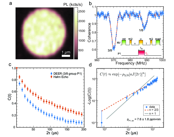
NV centers serve as excellent sensors of the local spin environment via dipolar interactions with nearby spins. In this work, we use the decoherence dynamics of a probe NV center ensemble to reveal characteristics of the surrounding P1 bath. We utilize double electron electron resonance (DEER) and Hahn spin echo measurements to accurately quantify the P1 center density, ,Eichhorn et al. (2019); Osterkamp et al. (2020); Davis et al. (2021) and confirm their dimensionality.Davis et al. (2021) Two-dimensionality is defined by a layer thickness that is smaller than the inter-spin spacing for a given dopant density. Fig. 2a shows a photoluminesence image of the TEM-irradiated, NV-rich spot on sample A (henceforth referred to as spot I). All NV-based measurements are performed on a home-built confocal microscope using a 532-nm diode laser and an external magnetic field of 310 G aligned along one of the NV <111> axes. Radiofrequency (RF) signals are delivered through a gold antenna fabricated on a glass coverslip and placed underneath the diamond.
Extraction of density and dimensionality
Through DEER-based sensing, we characterize the nitrogen spin bath by selectively probing the quasistatic contribution of P1 centers to NV decoherence. Fig. 2b shows a frequency-swept DEER spectrum of the hyperfine state of the 15N P1 centersEichhorn et al. (2019) revealing two peaks: the shallow peak (the 1/8 group) corresponds to the 15N P1 center with its Jahn-Teller axis aligned to the external magnetic field and the deeper peak (the 3/8 group) corresponds to the three other degenerate 15N P1 centers with Jahn-Teller axes misaligned to the field.Davies (1981) The DEER pulse sequence is illustrated in the inset of Fig. 2b. A pump pulse resonant with the 3/8 group of P1 centers with frequency fP1 recouples the P1 bath to the NV centers, and the resulting contribution to decoherence is read out via an NV center Hahn echo measurement. Essentially this sequence constitutes a Ramsey measurement of the NV-P1 interaction.
The timescale of the DEER decoherence decay provides information about the density of P1 centers, and the stretch exponent of the decay indicates the dimensionality of the spin bath. According to theory presented in Ref.Davis et al. (2021) the decoherence decay profile is expected to take the following form:
| (1) |
where is the density (in units of ppmnm for a 2D spin bath) of the driven group of P1 centers, is a dimensionless constant (that equals 2.626 for a 2D spin bath or 3.318 for a 3D spin bath), and is the dipolar coupling strength. The stretch power, , depends on the dimensionality of the system, , and the power law of the interactions, . Importantly, Eq. 1 is only valid at times short compared to the correlation time of the bath, i.e. . For a 2D spin bath coupled to the NV via dipolar interactions (), we expect when measuring on a time scale much shorter than ; for a 3D bath we expect as seen, e.g., in Ref.Davis et al. (2021). Further details on the theoretical analysis are given in the SI.
Fig. 2c plots the NV coherence as measured by Hahn echo and by DEER using a differential measurement scheme.Bluvstein et al. (2019b) The DEER data shows the expected reduction of coherence when recoupling the P1 centers. Fig. 2d plots the DEER decay normalized by the NV Hahn echo on a log-log scale as a function of free evolution time (). The DEER data is normalized by the Hahn echo in order to eliminate any contributions to decoherence from other sources. The excellent agreement of the data to a fit with stretch power of and poor agreement with confirms the two-dimensional nature of the spins.
The data also provide a quantitative estimate of the total P1 density, ppmnm in the TEM irradiation spot I. This density corresponds to a P1 spacing of 13.8 nm, larger than the layer thickness as measured by SIMS and hence consistent with a 2D spin system. Density measurements are averaged over six locations within TEM spot I, where the 1.8 ppmnm standard deviation reflects the variation across the spot. We attribute this variation to inhomogeneous nitrogen incorporation during growth, which will be a subject of future study. We note that the NV-DEER based estimate of is times lower than the SIMS measurement (60.1(0.5) ppmnm). This trend holds for the data collected on sample B as well, where the DEER-measured of 16 ppmnm is times less than the SIMS-estimated 89.5(0.8) ppmnm (full analysis in the SI). Given the uncertainties in the RSF value and the fact that SIMS measures all forms of nitrogen and is not specifically sensitive to P1 centers (as in DEER), this discrepancy is not surprising, and importantly, it confirms our understanding that SIMS needs a cross-referencing technique to more accurately determine the concentration of dopant atoms in our material.
III Characterization of NV center properties
We next move to characterizing the density, dimensionality, and coherence of NV centers formed via our growth and irradiation approach. In addition to enabling the study of strongly interacting, optically addressable spin ensembles in 2D for sensing and simulation, it also facilitates the creation of coherent NV centers with a specified, tunable density to realize e.g., a single NV per nanopillar in a scanning probe tipMaletinsky et al. (2012); Pelliccione et al. (2016) or a single NV inside of a photonic crystal cavity.Englund et al. (2010) Here we explore the creation and properties of the NV centers in our delta-doped system, finding both high NV/P1 ratios and remarkably long coherence which is predominantly limited by the P1 and NV environment.
NV center density estimation
A number of methods are typically used to estimate the NV center density, , when individual NV centers are not optically resolvable and countable. Broadly, these methods fall into two categories: the first involves probing the decoherence timescale of the NV ensemble under a specific RF pulse sequence, such as NV-NV DEER ,Eichhorn et al. (2019) instantaneous diffusion,Eichhorn et al. (2019) or an XY-8 sequence.Zhou et al. (2020) The second, all-optical method estimates density from the ensemble fluorescence intensity. However, these techniques all come with their drawbacks. The spin decoherence methods require long averaging times and are limited to dense NV ensembles where NV-NV dipolar interactions are comparable to or stronger than other sources of decoherence. Biased estimates can result when ensembles deviate from this high (NV-dominant) density, and pulse errors can introduce further bias (see SI for further explanation and the results of implementing these methods on samples A and B). Estimating density of NV ensembles via fluorescence can be hampered by unwanted background fluorescence from other irradiation-induced defects, which becomes particularly relevant at high electron dosages.
Here we introduce a simple and more reliable approach to determine the NV density. Our method benefits from not only its quick and easy implementation but also its large dynamic range which allows for density estimation from single NVs to high-density ensembles. We measure the fluorescence intensity difference between NV ensemble spin states ( and ) in a Rabi experiment and normalize by the corresponding signal from a single NV. By isolating the component of the fluorescence that changes with microwave driving, the measurement is immune to contributions from non-NV- defects. This method combines fluorescence counting and spin manipulation to measure a uniquely NV signal.
Briefly, our NV density estimation technique proceeds as follows (further details provided in the SI). First the point spread function (PSF) of the confocal setup is determined by fitting the fluorescence profile of an average of several single NV centers. Next, the PSF is convolved with a random distribution of 1 ppmnm NVs to calculate a spatial average of the resulting signal, . This average factor accounts for the fact that not all NV centers in the confocal spot reside at the center of the spot. Lastly is estimated by relating , the fluorescence intensity difference of the and states in a Rabi experiment, of single and ensemble NVs via:
| (2) |
The factor of four accounts for the four possible NV orientations, assuming an equal distribution among them, to yield as the total NV density.
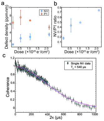
Applying this method to the TEM spot I, we find ppmnm averaged over eight different laser positions within the spot. The variation of across the spot is consistent with the variation observed in . In the SI, we compare measurements of in samples A and B obtained with our Rabi-assisted fluorescence method and spin decoherence methods, specifically NV-NV DEER and XY-8. Using our new method, we find to lie between the estimates produced by NV-NV DEER and XY-8 measurements; this trend is consistent with our expectations for the biases imposed by these two methods and advocates for the accuracy of our Rabi-assisted fluorescence measurement.
NV center creation and coherence
We next characterize across a range of electron irradiation dosages and importantly find a high NV/P1 ratio of up to 0.74, corresponding to of up to 3.50.4 ppmnm. Figs. 3a-b show a clear increasing trend of and NV/P1 ratio with electron dosage. The NV/P1 ratio is an important figure of merit for this work because the NV and P1 centers are the dominant contributors to decoherence in our samples, as will be discussed below. Further, and are quantitatively probed by our NV-based measurements. Interestingly, we observe higher NV/P1 ratios in our 2D delta-doped sample compared to 3D nitrogen-doped samples prepared via similar irradiation dosages and growth procedures (with longer doping times).Eichhorn et al. (2019) We posit that the higher NV/P1 ratios observed here are related to the dimensionality of the nitrogen layer and the diffusion of vacancies during annealing. In a 2D layer, each nitrogen interacts with a greater number of vacancies compared to the 3D case because of the finite diffusion volume during annealing. Thus, the enhancement will be determined by a dimensionless parameter given by , where is the diffusion volume and is the layer thickness.
To test the validity of this explanation, we construct a simple vacancy capture model (detailed in the SI) where vacancies migrate according to a weighted one-dimensional random walk and can be captured by an adjacent nitrogen with unit probability. Using our experimental parameters, we find a 15 enhancement of conversion for the 2D layer vs. the 3D layer, supporting the hypothesis that the geometrical diffusion effect is responsible for the observed enhancement in 2D. While this model does not attempt to rigorously simulate all aspects the NV center formation process, it supports our experimental findings of increased conversion in 2D-doped samples and suggests an interesting subject for future study.
Beyond the high NV/P1 ratios, a notable feature of the NV centers in our delta-doped samples is their long Hahn echo T2 coherence time across a range of P1 and NV defect densities (see SI Fig. S5). Maintaining long coherence is crucial for all the aforementioned experiments and applications in quantum sensing and simulation, particularly when operating in the dense P1 or NV regime. In the unirradiated regions, we find single, optically resolvable delta-doped NV centers in a dense P1 background, and we measure Hahn echo T2 times of 535 s, 562 s, and 489 s for three single NVs, a representative example of which is shown in Fig. 3c. This result is promising for applications such as NV scanning probe microscopy, which demands single-NV-containing probes formed with high yield. Higher density ensembles of NV centers in TEM spot I show an average coherence time of 10810 s, which is in good agreement with the expected decoherence from a bath of P1 and NV centers of the measured density (see SI for analysis of the P1 and NV contributions to decoherence). The dominance of intentional spin-spin interactions, combined with the system’s 2D nature, is critical for experiments in many-body sensing and simulation.
IV Conclusion
In this work, we have demonstrated the controlled creation and characterization of 2D spin systems in diamond with tunable density and long coherence. By harnessing slow growth rates and substrate miscut control, we achieve thin nitrogen layer confinement and characterize the P1 dimensionality and density with both SIMS and NV spin decoherence-based techniques, noting the importance of spin-based measurements in characterizing the relevant spin bath density. We demonstrate NV density tunable via electron irradiation and observe high NV/P1 ratios in the 2D system. NV density characterization is performed using a simple Rabi-assisted, fluorescence-based NV method introduced here that does not suffer from the biases of other estimation techniques and demonstrates a large dynamic range. Furthermore, we observe long NV T2 coherence times despite the rich P1 and NV environment, suggesting that the system is not severely limited by disorder from other defects. Altogether this work presents a careful materials and qubit-joint approach to engineer unique spin systems for enabling a variety of investigations in quantum sensing and simulation.
Supplementary Information
See the SI for additional details on the SIMS analysis, characterization of sample B, details of the Rabi-assisted density estimation and comparison to other methods, vacancy diffusion/NV creation model, additional coherence measurements and interpretation, and supporting information about the decoherence decay analysis.
Data Availability
The data that support the findings of this study are available from the corresponding author upon reasonable request.
Acknowledgements.
We gratefully acknowledge support of the U.S. Department of Energy BES grant No. DE-SC0019241 (materials growth and characterization), the Center for Novel Pathways to Quantum Coherence in Materials, an Energy Frontier Research Center funded by the U.S. Department of Energy, Office of Science, Basic Energy Sciences (coherence studies), and the Army Research Office through the MURI program grant number W911NF-20-1-0136 (theoretical studies). We acknowledge the use of shared facilities of the UCSB Quantum Foundry through Q-AMASE-i program (NSF DMR-1906325), the UCSB MRSEC (NSF DMR 1720256), and the Quantum Structures Facility within the UCSB California NanoSystems Institute. L. B. H. acknowledges support from the NSF Graduate Research Fellowship Program (DGE 2139319) and the UCSB Quantum Foundry. S. A. M. acknowledges support from Canada NSERC (AID 516704-2018) and the UCSB Quantum Foundry. E. J. D. acknowledges support from the Miller Institute for Basic Research in Science.References
- Degen et al. (2017) C. L. Degen, F. Reinhard, and P. Cappellaro, Rev. Mod. Phys. 89, 35002 (2017).
- Schirhagl et al. (2014) R. Schirhagl, K. Chang, M. Loretz, and C. L. Degen, Annu. Rev. Phys. Chem. 65, 83 (2014).
- Rondin et al. (2014) Rondin, J.-P. Tetienne, T. Hingant, J.-F. Roch, P. Maletinsky, and V. Jacques, Rep. Prog. Phys. 77, 56503 (2014).
- Casola et al. (2018) F. Casola, T. V. D. Sar, and A. Yacoby, Nat. Rev. Mater. 3, 1 (2018).
- Rovny et al. (2018) J. Rovny, R. L. Blum, and S. E. Barrett, Phys. Rev. Lett. 120, 180603 (2018).
- Cappellaro and Lukin (2009) P. Cappellaro and M. D. Lukin, Phys. Rev. A. 80, 032311 (2009).
- Yao et al. (2014) N. Y. Yao, C. R. Laumann, S. Gopalakrishnan, M. Knap, M. Müller, E. A. Demler, and M. D. Lukin, Phys. Rev. Lett. 113, 243002 (2014).
- Choi et al. (2017) S. Choi, J. Choi, R. Landig, G. Kucsko, H. Zhou, J. Isoya, F. Jelezko, S. Onoda, H. Sumiya, V. Khemani, C. von Keyserlingk, N. Y. Yao, E. Demler, and M. D. Lukin, Nature 543, 221 (2017).
- Choi et al. (2020) J. Choi, H. Zhou, H. S. Knowles, R. Landig, S. Choi, and M. D. Lukin, Phys. Rev. X. 10, 031002 (2020).
- an S. A. Dzuba and Raitsimring (1981) K. M. S. an S. A. Dzuba and A. M. Raitsimring, J. Mag. Res. 42, 255 (1981).
- Yao et al. (2018) N. Y. Yao, M. P. Zaletel, D. M. Stamper-Kurn, and A. Vishwanath, Nat. Phys. 14, 405 (2018).
- Chomaz et al. (2019) L. Chomaz, D. Petter, P. Ilzhöfer, G. Natale, A. Trautmann, C. Politi, G. Durastante, R. M. W. van Bijnen, A. Patscheider, M. Sohmen, M. J. Mark, and F. Ferlaino, Phys. Rev. X. 9, 021012 (2019).
- Burin (2015) A. L. Burin, arXiv:1409.7990 [cond-mat, physics:quant-ph] (2015), arXiv:1409.7990 [cond-mat, physics:quant-ph] .
- Abanin et al. (2019) D. A. Abanin, E. Altman, I. Bloch, and M. Serbyn, Rev. Mod. Phys. 91, 021001 (2019).
- Perlin et al. (2020) M. A. Perlin, C. Qu, and A. M. Rey, Phys. Rev. Lett. 125, 223401 (2020).
- Davis et al. (2021) E. Davis, B. Ye, F. Machado, S. Meynell, T. Mittiga, W. Schenken, M. Joos, B. Kobrin, Y. Lyu, D. Bluvstein, S. Choi, C. Zu, A. C. B. Jayich, and N. Y. Yao, “Probing many-body noise in a strongly interacting two-dimensional dipolar spin system,” (2021), arxiv:2103.12742.
- Degen et al. (2021) M. J. Degen, S. J. H. Loenen, H. P. Bartling, C. E. Bradley, A. L. Meinsma, M. Markham, D. J. Twitchen, and T. H. Taminiau, Nat. Comm. 12, 3470 (2021).
- Zhou et al. (2020) H. Zhou, J. Choi, S. Choi, R. Landig, A. M. Douglas, J. Isoya, F. Jelezko, S. Onoda, H. Sumiya, P. Cappellaro, H. S. Knowles, H. Park, and M. D. Lukin, Phys. Rev. X 10, 031003 (2020).
- Tetienne et al. (2018) J.-P. P. Tetienne, R. W. D. Gille, D. A. Broadway, T. Teraji, S. E. Lillie, J. M. McCoey, N. Dontschuk, L. T. Hall, A. Stacey, D. A. Simpson, and L. C. L. Hollenberg, Phys. Rev. B. 97, 085402 (2018).
- Kawai et al. (2019) S. Kawai, H. Yamano, T.Sonoda, K. Kato, J. J. Buendia, T. Kageura, R. Fukuda, T. Okada, T. Tanii, T. Higuchi, M. Haruyama, K. Yamada, S. Onoda, T. Ohshima, W. Kada, O. Hanaizumi, A. Stacey, T. Teraji, S. Kono, J. Isoya, and H. Kawarada, J. Phys. Chem. C 123, 3594–3604 (2019).
- Bluvstein et al. (2019a) D. Bluvstein, Z. Zhang, and A. C. B. Jayich, Phys. Rev. Lett. 122, 76101 (2019a).
- Myers et al. (2014) B. A. Myers, A. Das, M. C. Dartiailh, K. Ohno, D. D. Awschalom, and A. C. B. Jayich, Phys. Rev. Lett. 113, 027602 (2014).
- Findler et al. (2020) C. Findler, J. Lang, C. Osterkamp, M. Nesládek, and F. Jelezko, Sci. Rep. 10, 1 (2020).
- Ohno et al. (2012) K. Ohno, J. Heremans, L. Bassett, B. Myers, D. Toyli, A. B. Jayich, C. Palmstrom, and D. Awchalom, Appl. Phys. Lett 101, 082413 (2012).
- Bogdanov et al. (2021) S. Bogdanov, A. Gorbachev, D. Radishev, A. Vikharev, M. Lobaev, S. Bolshedvorskii, V. Soshenko, S. Gusev, D. Tatarskiy, and A. Akimov, Phys. Status Solidi RRL 2021, 15, 2000550 (2021).
- Jaffe et al. (2020) T. Jaffe, M. Atrash, M. Kuntumalla, R. Akhvlediani, S. Michaelson, L. Gal, N. Felgen, M. Fischer, J. Reithmaier, C. Popov, A. Hoffman, and M. Orenstein, Nano. Lett. 20, 3192 (2020).
- Lobaev et al. (2017) M. A. Lobaev, A. M. Gorbachev, S. A. Bogdanov, A. L. Vikharev, D. B. Radishev, V. A. Isaev, V. V. Chernov, and M. N. Drozdov, Diam. Rel. Mater. 72, 1 (2017).
- Lobaev et al. (2018) M. A. Lobaev, A. M. Gorbachev, S. A. Bogdanov, A. L.Vikharev, D. B. Radishev, V. A. Isaev, and M. N. Drozdov, phys. stat. sol. (a) 215, 1800205 (2018).
- McLellan et al. (2016) C. A. McLellan, B. A. Myers, S. Kraemer, K. Ohno, D. D. Awschalom, and A. C. B. Jayich, Nano. Lett. 16, 2450 (2016).
- Eichhorn et al. (2019) T. Eichhorn, C. McLellan, and A. C. B. Jayich, Phys. Rev. Mater. 3, 113802 (2019).
- Farfurnik et al. (2017) D. Farfurnik, N. Alfasi, S. Masis, Y. Kauffmann, E. Farchi, Y. Romach, Y. Hovav, E. Buks, and N. Bar-Gill, Appl. Phys. Lett. 111, 123101 (2017).
- Bogdanov et al. (2019) S. A. Bogdanov, A. M. Gorbachev, D. B. Radishev, A. L. Vikharev, M. A. Lobaev, S. A. Gusev, D. A. Tatarsky, S. V. Bolshedvorskii, A. V. Akimov, and V. V. Chernov, Tech. Phys. Lett. 45, 281 (2019).
- Achard et al. (2020) J. Achard, V. Jacques, and A. Tallaire, J. Phys. D: Appl. Phys. 53, 313001 (2020).
- de Theije et al. (2000) F. K. de Theije, J. Schermer, and W. J. P. van Enckevort, Diam. Rel. Mater. 9, 1439 (2000).
- Tallaire et al. (2015) A. Tallaire, M. Lesik, V. Jacques, S. Pezzagna, V. Mille, O. Brinza, J. Meijer, B. Abel, J. F. Roch, A. Gicquel, and J.Achard, Diam. Rel. Mater. 51, 55 (2015).
- Meynell et al. (2020) S. Meynell, C. McLellan, L. B. Hughes, W. Wang, T. E. Mates, K. Mukherjee, and A. C. B. Jayich, Appl. Phys. Lett. 117, 194001 (2020).
- Koike et al. (1992) J. Koike, D. M. Parkin, and T. E. Mitchell, App. Phys. Lett. 60, 1450 (1992).
- Campbell and Mainwood (2000) B. Campbell and A. Mainwood, phys. stat. sol. 181, 99 (2000).
- Ziegler et al. (2010) J. F. Ziegler, M. D. Ziegler, and J. P. Biersack, Nuclear Instruments and Methods in Physics Research B 268, 1818 (2010).
- Wilson and Novak (1991) R. Wilson and S. Novak, J. Appl. Phys. 69, 466 (1991).
- Ranjan et al. (2020) V. Ranjan, S. Probst, B. Albanese, T. Schenkel, D. Vion, D. Esteve, J. J. L. Morton, and P. Bertet, App. Phys. Lett. 116, 184002 (2020).
- Osterkamp et al. (2020) C. Osterkamp, P. Balasubramanian, G. Wolff, T. Teraji, M. Nesladek, and F. Jelezko, Adv. Quan. Tech. 3, 1 (2020).
- Davies (1981) G. Davies, Rep. Prog. Phys. 44, 788 (1981).
- Bluvstein et al. (2019b) D. Bluvstein, Z. Zhang, C. A. McLellan, N. R. Williams, and A. C. B. Jayich, Phys. Rev. Lett. 123, 146804 (2019b).
- Maletinsky et al. (2012) P. Maletinsky, S. Hong, M. S. Grinolds, B. Hausmann, M. D. Lukin, R. L. Walsworth, M. Loncar, and A. Yacoby, Nat. Nanotech. 7, 320 (2012).
- Pelliccione et al. (2016) M. Pelliccione, A. Jenkins, P. Ovartchaiyapong, C. Reetz, and A. C. B. Jayich, Nat. Nanotech. 11, 700 (2016).
- Englund et al. (2010) D. Englund, B. Shields, K. Rivoire, F. Hatami, J. Vuckovic, H. Park, and M. D. Lukin, Nano Lett. 10, 3922 (2010).