Electronic Poiseuille Flow in Hexagonal Boron Nitride Encapsulated Graphene FETs
Electronic Poiseuille Flow in Hexagonal Boron Nitride Encapsulated Graphene FETs
Abstract
Electron-electron interactions in graphene are sufficiently strong to induce a correlated and momentum-conserving flow such that charge carriers behave similarly to the Hagen-Poiseuille flow of a classical fluid. In the current work, we investigate the electronic signatures of such a viscous charge flow in high-mobility graphene FETs. In two complementary measurement schemes, we monitor differential resistance of graphene for different channel widths and for different effective electron temperatures. By combining both approaches, the presence of viscous effects is verified in a temperature range starting from 178 K and extending up to room temperature. Our experimental findings are supported by finite element calculations of the graphene channel, which also provide design guidelines for device geometries that exhibit increased viscous effects. The presence of viscous effects near room temperature opens up avenues for functional hydrodynamic devices such as geometric rectifiers like a Tesla valve and charge amplifiers based on electronic Venturi effect.
I Introduction
The dynamics governing the flow of charges in conductors is heavily dependent on the ratios of the different physical length scales present in the system. These length scales dictate how the charge carriers interact with each other, with the system boundaries, and with defects or impurities. Microscopically, the flow of charge carriers is resisted by scattering from defects and lattice vibrations (phonons), characterized by the length scale, , which is the average distance traveled by the charge carriers between two such momentum-relaxing (inelastic) scattering events. The charge carriers also interact with each other in a momentum-conserving (elastic) fashion, with a length scale, . The third relevant length scale is the channel width, (assuming channel length ), dictating how often charge carriers interact with the boundary of the system.
In most conductors, diffusive scattering prevails () and charge transport is Ohmic. Charge carriers traveling across the channel suffer many momentum relaxing collisions leading to a constant drift velocity along the direction of the applied electric field [1]. Alternatively, transport is ballistic, when the channel dimensions are the smallest length scale in the system. Under these circumstances, charge carriers travel collision-less from the source to the drain terminal, dissipating energy only at the contacts [2]. However, a third, and relatively unexplored transport regime emerges, when inter-particle scattering dominates (). These strong inter-particle interactions lead to a correlated, viscous charge flow, similar to the flow of fluids and governed by the theory of hydrodynamics [3, 4, 5, 6, 7, 8, 9, 10]. A direct consequence of this behavior is the non-uniformity of the carrier velocity in the channel, which follows a Poiseuille-like flow profile, similar to fluids (Fig. 1a). In the context of electrical transport, this translates to a (non-uniform) position dependent current density, being largest in the center of the channel and decreasing on approaching the channel edges, following a parabolic profile.
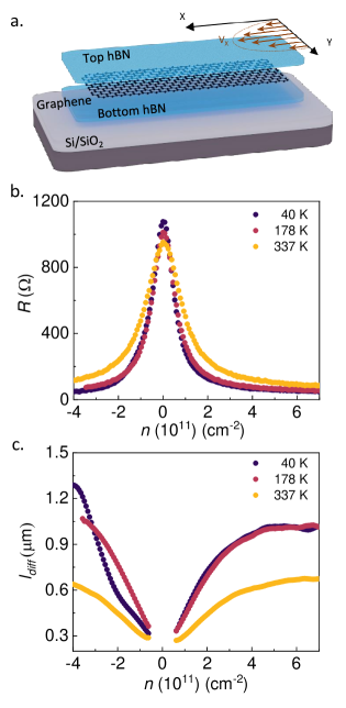
Fulfilling the criteria of charge hydrodynamics requires high mobility devices with reduced scattering from defects and phonons (large ) and strong inter-particle interactions (small , generally observed in materials with a simple Fermi surface). Graphene fulfills both these requirements. First, the electron-electron interaction strength is enhanced by the nearly circular Fermi surface at low number densities (small ) [11, 12]. Second, graphene has a weak electron-phonon coupling strength [13, 14, 15] and advancements in fabrication techniques make it possible to limit scattering from extrinsic disorders, in particular by encapsulation in hexagonal boron nitride (-BN). -BN also serves as an ideal substrate for graphene, due to its atomically flat surface and low lattice mismatch () [16] (Fig. 1a). These lead to graphene heterostructures having outstanding electronic properties and large .
In recent years, hydrodynamic transport of charge has attracted significant theoretical attention [5, 17, 18, 19, 20], and several experimental signatures have been reported [21, 22, 23, 6, 7, 8]. Of particular interest is the direct observation of the parabolic flow profile. Recent investigations utilizing direct imaging of Hall field [24] and local magnetic field [22, 25] have hinted at the presence of viscous effects in charge transport in graphene and layered Weyl semimetals. Additionally, unique transport properties like formation of vortices, negative local resistance and superballisticity have also been linked to a hydrodynamic charge flow [26, 6, 23]. Apart from the Coulomb mediated electron-electron interactions [5, 17, 18, 19, 20], recent reports also indicate the possibility of phonon mediated electronic interactions generating a correlated charge flow at higher carrier densities [26, 25]. Though electrical signatures of Poiseuille flow in graphene have been reported [6, 23], a comparative study of the transport signatures from multiple types of experiments and a determination of the temperature range for the viscous effects is lacking.
In the current work, we perform electrical transport measurements in -BN encapsulated graphene field effect transistors () to investigate the presence of electronic Poiseuille flow. For this purpose two separate measurement schemes are used, 1. Current Bias measurements (Section III) and 2. Width dependent measurements (Section IV). For the current bias measurements, we look into the scaling of channel resistance as a function of DC bias current in a sample of constant width (schematic in Fig. 2a). The width dependent measurements investigate the flow of charge carriers in channels of different widths (schematic in Fig. 3a). We observe signatures of correlated charge flow for temperatures starting from K and persisting upto 300 K. Further, finite element calculations are performed to verify the experimental observations (Section V). Our results demonstrate the presence of strong electronic correlations near room temperature opening up possibilities of utilizing the viscous electronic flow in graphene for functional devices.
II Electrical performance of
The quality of the fabricated was assessed by measuring the conductance of the channel as a function of gate voltage, as called a transfer characteristic at different temperatures (Fig. 1b). The devices were fabricated using a standard dry transfer technique [27] and measurements performed in a four-probe geometry to remove the contact resistance (See Methods). -BN encapsulation allows fabrication of edge-contacts, which are known to outperform conventional surface contacts [28]. Fig. 1b demonstrates a typical graphene transfer characteristic, with a maximum of resistance near the Dirac point and a sharp decrease with increasing number density (). This corresponds to the transition from insulating behavior, caused by the formation of charge puddles near the neutrality point, to metallic behavior [29, 30]. The high quality of our FETs is demonstrated by a large carrier mobility () (Supplementary Fig. S1) and a large 1 m (Fig. 1c), thereby relaxing the criteria for hydrodynamic behavior () for properly designed channels. The value of is computed considering a Drude model,
| (1) |
where, is the channel conductivity, the cyclotron mass [31] and ms-1, the Fermi velocity of graphene. We observe a reduction in the with increasing temperature (especially at 337 K) which can be attributed to increased momentum relaxing scattering events [16]. Temperature dependence of is provided in Supplementary Fig. S1.
III Current Bias Measurements
With the high quality of our established, we turn to current bias measurements which consist of measuring the device conductance for increasing DC bias current. The role of the DC bias ( A) is to increase the electronic temperature of the devices, thereby providing a knob to increase the inter-particles interactions and reduce . At the same time, the weak electron-phonon coupling in SLG ensures the lattice temperature does not significantly increase, which would lead to an increase in diffusive scattering processes, and hence a decrease in [13, 14, 15]. The decoupling of the two length scales therefore creates an ideal scenario for hydrodynamic charge flow [9].
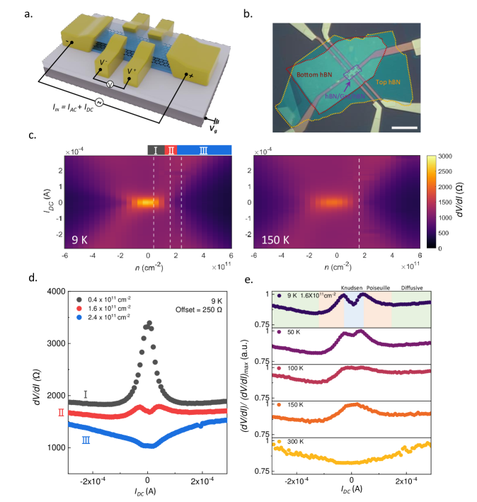
Fig. 2a presents the device geometry and circuit connections used for the current bias measurements and Fig. 2b is an optical micrograph of the measured device. The measured device has a channel length and width of 1.1 m and 0.55 m, respectively. The transfer characteristics, mobility and of the device are presented in Supplementary Fig. S2. Fig. 2c shows color plots of d/d as a function of and recorded at 9 K and 150 K. At K, for changing number densities, three types of curves are observed. The number densities in which these behaviors are observed are indicated above the color plot. For each behavior, a typical curve is plotted in Fig. 2d, with the number densities highlighted by the vertical dashed lines in Fig. 2c . For low (Scaling behavior \@slowromancapi@), the d/d values follow a monotonic decreasing trend with increasing until about A ( mA/m). For larger values of , the curve is stable with only a minute increase in resistance. This behavior results in a central bright spot in the color map. With increasing , we observe a non-monotonicity in the measured d/d, as apparent from the central bright spot that splits into two ridges and a valley appearing in the center (Scaling behavior \@slowromancapii@).
For Scaling behavior \@slowromancapii@, the curves exhibit three distinct regions. First, for low DC currents, the d/d values increase with current. d/d then reaches a peak and in the second region, decreases for increasing current (reaching a minimum of d/d), while in the third region, d/d steadily increases with DC current. The experimentally observed non-monotonicity in the differential resistance hints towards the presence of viscous effects ( cm-2 in Fig. 2d), as we will discuss later on. Finally, for the largest (Scaling behavior \@slowromancapiii@), the negative slope region vanishes and the d/d is constant for small with a monotonic increase for higher current values.
The three different Scaling behaviors with changing can be rationalized as follows. For Scaling behavior \@slowromancapi@, electrical transport is dominated by the formation of charge puddles, leading to an insulating behavior at low DC currents, with a transition to metallic behavior for increasing DC current [29, 30, 32, 33]. The initial drop in resistance is associated with electric field assisted interband carrier generation [32]. We can calucate the charge inhomogeneity () near the Dirac point from the minima in the d/d. This gives cm-2, which is similar to those reported in encapsulated graphene [33]. The metallic behavior at higher has been attributed to a Schwinger production of electron hole plasma in graphene [33]. For Scaling behavior \@slowromancapii@, increasing the DC current leads to three distinct regions in the curve in which the charge transport is quasi-ballistic/Knudsen, hydrodynamic/Poiseuille and diffusive, respectively. For low DC currents, the charge carriers flow nearly collisionless, leading to a quasi-ballistic transport, also known as the electronic Knudsen regime. The transfer characteristics also indicate the presence of quasi-ballistic transport (Supplementary Fig. S2). Upon increasing , the electron temperature increases and consequently the inter-particle collisions are increased. Even though such collisions are momentum conserving and lead to no resistance, they make it more probable for the carriers to reach and diffusively interact with the sample boundaries [9], leading to an increase in the resistance (d(d/d)/d). A further increase in until brings about a transition to the Poiseuille regime. Here, the inter-particle collisions actively prevent a large fraction of the charge carriers (ones near the center of the channel) from seeing the boundaries, resulting in a slope reversal, d(d/d)/d, and a minimum in the differential resistance. This negative slope for intermediate and minima of d/d in clean conductors are signatures of the electronic Gurzhi effect [34]. This has been experimentally observed previously and is indicative of the presence of viscous/Poiseuille flow [6, 9]. This regime lasts until diffusive scattering processes within the sample gain prominence, restoring the positive slope of d/d as expected in standard metallic behavior or the diffusive regime (d(d/d)/d). A similar behavior is observed in four different samples (See Methods for details). Finally, for higher number densities (Scaling behavior \@slowromancapiii@), the inter-particle interactions are screened (larger ) [35, 36] while the diffusive scattering remains largely unaffected (constant in Supplementary Fig. S2 and Fig. 1c) [6]. A combination of these effects leads to the vanishing of the Poiseuille flow (negative slope of d/d). The d/d values are nearly constant for low (quasi-ballistic regime) and show an increasing trend once diffusive scattering starts dominating the transport around DC currents of A (0.05 mA/m). Similar observations were also made for hole transport in (negative ), and are presented in Supplementary Fig. S3.
We also investigate the effect of the lattice temperature () on the Gurzhi effect by recording the conductance maps at different temperatures. The color plots at all temperatures are presented in Supplementary Fig. S4. First, we compare the conductance map at 150 K (Fig. 2c (right panel)) to the one obtained at 9 K (Fig. 2c (left panel)). Two major differences are observed. First, the central bright spot has a reduced intensity and, second, the Knudsen flow is absent for higher values. Color plots at intermediate temperatures are presented in the Supplementary Fig. S4. The reduction in intensity of the central bright spot is indicative of a reduced Dirac point resistance at higher values of in . This is an effect of the enhanced particle-hole excitation, similar to our observations in Fig. 1b. The disappearance of the Knudsen regime is better visualized when the curves for an intermediate number density of 1.61011 cm-2 are investigated for all temperatures (Fig. 2e). At low , all three regimes, Knudsen, Poiseuille and diffusive are visible. However, with increasing , the Knudsen regime first reduces in size, until it disappears at 150 K. Thereafter, at 300 K, the Poiseuille regime also vanishes and the only demonstrate signatures of diffusive transport.
This -dependence can be understood by considering the variation of and with lattice temperature. At K, , which results in a quasi-ballistic or Knudsen flow persisting upto large values of (Supplementary Fig. S2). A transition from Knudsen to Poiseuille flow occurs when . With increasing , the Poiseuille flow condition is satisfied at smaller values of , leading to a diminishing Knudsen flow regime. This trend persists until the lattice temperature is high enough for the sample to enter the Poiseuille flow regime at 0. This is indicated by the absence of the Knudsen regime and is observed at 150 K (Supplementary Fig. S2). The sample remains in the Poiseuille regime until diffusive scattering processes gain prominence () and the differential resistance shows a monotonic positive slope (300 K data in Fig. 2e). Our differential resistance measurements, thus, hint towards the presence of a viscous Poiseuille flow in at temperatures between 150 and 300 K.
IV Width Dependent Measurements
In addition to differential resistance measurements, we also verify the presence of Poisuille flow using geometric effects in the channel conductivity (). For diffusive transport, is a material parameter and therefore the current density (J) is uniform across the device cross-section. However, in the Poiseuille regime, the parabolic profile of J (or carrier velocity) (Fig. 1a) manifests itself as a strong width-dependence in . For a 2D Fermi Liquid in the Poiseuille regime, the transport equations are given by [20]
| (2) |
| (3) |
where, Eq. 2 and Eq. 3 are the electrical analogues of the continuity and Navier-Stokes equations, respectively. is the Drude conductivity, the electric potential and the electronic charge. , the Gurzhi length, is a charcteristic length scale determining the strength of viscous effects. Its functional dependence is given by
| (4) |
where, is the kinematic viscosity. The second term of Eq. 3 is the viscous term and is responsible for the geometry dependence of . An analytical relation for is obtained by solving Eq. 2 and Eq. 3 with a diffusive/no-slip boundary condition. The resulting functional dependence is
| (5) |
From Eq. 5, we can define an asymptotic limit of strong Poiseuille flow using the condition . In this case, we obtain, . This scaling of has been reported previously in the Fermi liquid of Weyl semimetals [8]. However, comparing the values of used in the current work (m) and previously reported values of m in graphene [6], we expect that the measured do not satisfy the conditions for strong Poiseuille flow. Hence, unlike previous reports [8], we find it suitable to fit the experimental with the non-asymptotic relation given by Eq. 5.
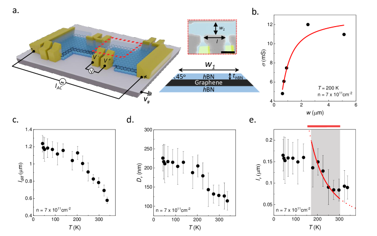
Fig. 3a shows a schematic of the used for our width-dependent measurements. To fabricate these devices, the -BN encapsulated graphene heterostructure was shaped into channels of different widths using reactive ion etching (RIE) (See Methods). Channel widths () and lengths () were confirmed by scanning electron micrographs (top right panel of Fig. 3a). The actual channel width () was estimated from the observed width (), plus taking into consideration the height of the top -BN and the 45 degree angle generated by the RIE process (bottom right panel of Fig. 3a) [28]. The width-dependent fitting allows us to extract several flow parameters, providing further insight into the viscous charge transport in . A detailed discussion of the process is presented below.
The transfer characteristic and of the width dependent device is presented in Fig. 1b and c, respectively. Fig. 3b shows the fitting of for lattice temperature K and cm-2. This particular choice of and is guided by previous reports of viscous effects in graphene at similar values of these parameters [6]. The closed circles are measured values of , while the solid line is a fit following Eq. 5, with and as fitting parameters. From the fit, one can directly extract the values of and . The extracted value of enables us to compute the diffusive mean free path using Eq. 1. We find m, which is a common occurrence in high quality graphene devices (Fig. 3c) [6, 28]. The value of m (Fig. 3d), obtained from the fit is also in close agreement with previous reports [6]. Substituting and in Eq. 4 gives us an estimate of the viscosity () of the charge carriers. We obtain a high kinematic viscosity, m2s-1 (K), making the flow more viscous than honey, a phenomenon which has been reported previously (Supplementary Fig. S5) [6]. This high viscosity is also one of the assumptions for using the linearized Navier-Stokes equation in Eq. 3. Additionally, the flow viscosity, which arises due to the inter-particle scattering, can be directly related to the viscous mean free path, , a parameter which is closely related to [6, 19]. The exact relationship at low excitation frequencies ( Hz) is given by
| (6) |
The extracted m at K, is the smallest length scale in the system (), indicative of the presence of Poiseuille flow in at K (Fig. 3e). To explore further, we repeat the width-dependent measurements at different lattice temperatures and explore the temperature dependence of , , and in Fig. 3c, d, e and Supplementary Fig. S5, respectively. The flow parameters demonstrate a dependence only in an intermediate temperature range of K and saturate (except for ) for K and K.
To understand the physical relevance of these values, we compare the extracted with its predicted dependence for the Dirac fermionic liquid in a doped graphene sheet [19]. The analytical relation for is given by
| (7) |
where, is the number of Fermionic flavours in graphene, the fine structure constant and the Boltzmann constant. is computed from the relation [19, 37]
| (8) |
where is the electrical permittivity. For the current work, we have used the permittivity of BN considering a dielectric constant of 4 [38]. Eq. 7 (solid line in Fig. 3e) has no fitting parameters and matches the extracted values of (closed circles in Fig. 3e) for the intermediate temperature range, 300 K (shaded region in Fig. 3e). The extracted flow parameters are thus physically relevant only for these intermediate temperatures. Additionally, we note that the assumptions of viscous flow made in the formulation of the transport equations (Eq. 2 & 3) limit their validity, and as a result, the validity of the geometry dependent analysis for values of where Poiseuille flow is present. In combination, the physical relevance of the extracted flow parameters and the validity of the viscous flow equations confirm the presence of Poiseuille flow for K in . Finally, this observation is strengthened by the fact that similar values are obtained for both the current bias measurements (Section III) and width dependent measurements (Fig. 2e and Fig. 3e). We also look at the number density dependence of the flow parameters in Suppementary Fig. S6. The geometry dependent measurements indicate the presence of hydrodynamic effects for number densities cm-2. Further discussions are provided in Suppementary Fig. S6.
V Finite element methods
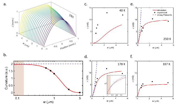
Finally, we turn to finite element calculations (implemented in Comsol Multiphysics 5.6) to model the Poiseuille flow in . This process involves numerically solving Eq. 2 and 3 with an uniform electric field () and no-slip boundary conditions for different values of . The input parameters, and , are calculated from the theoretical predictions of (Eq. 7) and the field effect mobility (). Our channels are oriented along the x-axis while their width follows the y-axis. An example of a simulated flow profile is depicted in Fig. 4a for K. We observe strong Poiseuille effects for small channel widths, indicated by the parabolic dependence of the normalized current density () on the normalized channel position (), and a weak Poiseuille flow, indicated by a constant , for larger values of . The curvature of the flow profile computed at the center of the channel () also exhibits a width dependence (solid line in Fig. 4b). It saturates to a value of 2 for the smallest widths with a parabolic flow profile (m in Fig. 4a) and reduces to 0 for larger widths with a constant (m in Fig. 4a). The filled circles in Fig. 4b correspond to the measured values of in the current work. Further, we extract the channel conductivity () from the simulated flow profile. In Fig. 4c to f, the simulated (solid red line) and experimental (filled circles) values of are compared for four different values of . The simulated results match experimental data for temperatures in the Poiseuille flow regime ( and K), with mismatches at lower ( K) and higher ( K) temperatures, where our experiments indicate the absence of hydrodynamic effects.
In what follows, we quantify our observations and predict the values of necessary for a strong Poiseuille flow. As discussed before, the strong Poiseuille regime is characterized by a scaling of . This is indicated by the dashed blue lines in Fig. 4d and e, computed with the same parameter values as in the simulation (solid red line). Indeed, the experimentally measured widths in our devices are too large for observing this effect as the flow is in the weak Poiseuille regime. The strong Poiseuille regime is determined by computing the relative difference between the simulated (solid red line) and strong Poiseuille (dashed blue line) values of . Values of for which the relative difference remains below 10% are considered to be in the strong Poiseuille regime. The criteria is satisfied for m, indicated by the shaded region in the inset of Fig. 4d. Another indicator of the strong Poiseuille regime is the saturation of the flow curvature to a value of 2 (shaded region in Fig. 4b). In conclusion, our finite element model confirms our are in the weak Poiseuille regime and predicts strong Poiseuille flow for m in . Comparing the measured values of (Fig. 3e) with the computed length scale for strong hydrodynamics, we would expect this behavior to be present at a slightly higher temperature than the range indicated in the current work in order to satisfy the criteria .
VI Discussions and Conclusions
Strikingly, we observe hydrodynamic effects at different charge number densities in the geometry dependence study ( cm-2) (Supplementary Fig. S6) and the current bias measurements ( cm-2), for which we have no clear, unique explanation. Similar behavior has been seen in previous reports, with current bias measurements showing viscous effects for lower number density ranges compared to negative vicinity resistance [6]. This could indicate either a number density selectivity in the transport probes of charge hydrodynamics or a number density variability of the hydrodynamic regime in graphene.
In conclusion, we demonstrate the electrical signatures of Poiseuille flow in charge transport through graphene channels using the Gurzhi effect and geometry dependent measurements. We observe a negative slope in the differential resistance measurements and a strong geometry dependence of the channel conductivity, both indicative of the presence of viscous effects. The two different measurements types, in conjunction, enable us to define a temperature range for the viscous effects to occur, which reaches as high as 300 K. Moreover, we provide an electrical transport-based characterization framework for detecting Poiseuille flow in conductors that can easily be extended to other conductors. Our experimental observations are corroborated by finite-element calculations that shed light on the channel geometries required for a strong Poiseuille flow. Our findings offer promising prospects for functional hydrodynamic graphene devices in the near future, such as geometric rectifiers like Tesla valves and charge amplifiers based on the electronic Venturi effects [39, 40, 41].
VII Methods
VII.1 Device Fabrication
measured in the current work are fabricated using the following process: the heterostructure assembly begins with the mechanical exfoliation of individual layers from bulk crystals (the graphite is obtained commercially from NGS Trading & Consulting GmbH and the -BN is from our co-authors in National Institute for Materials Science, Japan). Exfoliated flakes are optically screened using an optical microscope (Zeiss Axio Imager M2m). The layer number and quality of grphene flakes are determined using Raman spectroscopy (See Supplementary Fig. S7). We use a Raman system with a backscattering geometry confocal Raman microscope (WITec, Alpha 300 R). An excitation laser with a wavelength of 532 nm from a diode laser is used for all Raman measurements. The thickness of BN layers is characterized using atomic force microscopy in the tapping mode (Bruker Icon3 AFM). Selected flakes are aligned and stacked layer by layer using commercially available micromanipulator (hq Graphene 2D Heterostructure Transfer System). The pick-up process is performed using PDMS backed polycarbonate (PC) stamps. PC shows good adherence to -BN for KK. After successful pick-up of the top -BN layer, the middle graphene layer and bottom -BN layer are picked up using the van der Waals interaction between the different two-dimensional materials. Finally, the heterostructure is deposited on a pre-patterned Si++/ SiO2 (285 nm) wafer at K. The PC is dissolved in dchlorometane (DCM). The transfer process followed is similar to that in Ref. [27]. Following this, a thermal annealing step is performed at 650 K with H2/Ar 35/200 sccm for 3 hours to improve the quality of the heterostructures by reducing interfacial bubbles, contaminants etc. (See Supplementary Fig. S8 and S9). The small electrodes are defined using EBL and RIE (CHF sccm, O sccm, mTorr, Power = 60 W). Next, we deposit 5/25 nm Cr/Au directly using ebeam evaporator for edge-contacted electrodes and the pattern is lifted off using acetone for 45 min [28]. After that, the second EBL and metals deposition (5/65 nm Cr/Au) are performed for contact pads. Finally, we perform the third ebeam processing, followed by the second RIE for defining the channel shape. The morphology of the device is recorded by the same optical microscope mentioned above. Channel widths of devices are acquired from SEM (Hitachi S-4800). For the width dependent device the channel width () was varied while keeping the channel length constant.
For the current bias measurements, four devices on four different chips were fabricated. All samples demonstrate a similar scaling of d/d at base temperature. We observe the current biasing measurements have a tendency to generate irreversible hysteresis and electron doping (shifting of the Dirac point to negative gate voltages) in devices. Due to this we could perform the temperature characterization in one device and partial temperature characterization in a second device.
For the width dependent measurements, the largest four values of are from a single large graphene channel which was shaped into channels of different widths, while the smallest value is obtained from a second device on a different chip made following similar fabrication protocols.
VII.2 Measurement Details
The four-probe resistance of was measured using a lock-in technique, with an AC source-drain current ( of nA (231.45 Hz); ) while measuring the resulting voltage drop (Lockins used are SRS 830 or EG&G 7265). The SRS CS580 voltage controlled current source is used to supply to the sample. The gate voltage is supplied by an AdWin Gold \@slowromancapii@ connected to a voltage amplifier (Physics Basel SP 908). From the applied gate voltage, the number density is computed using [42], where, is the oxide capacitance (series combination of SiO2 (285 nm) and bottom -BN), is the electron charge, and are the gate and the Dirac point voltage, respectively.
For the current bias measurements, the DC bias is supplied by an AdWin Gold \@slowromancapii@ and the AC bias by a lockin. The two bias voltages are added using a summing amplifier SIM980. The current source CS580 converts the summed voltage to the supplied current bias. An nA (231.5 Hz) is used for the measurements and the output voltage from the sample measured using the lockin.
The width dependent measurements follow similar measurement technique as the transfer characteristic measurements.
The current bias measurements are carried out on a closed cycle manual probe station (Lakeshore). For width dependence measurements, the samples are wire bonded to a chip carrier and measured in a commercially available closed cycle cryostat from Advanced Research Systems (ARS).
VIII Acknowledgement
W.H., T.P. and M.C. acknowledge funding from the Swiss National Science Foundation under the Sinergia grant no. 189924 (Hydronics). K.W. and T.T. acknowledge support from the JSPS KAKENHI (Grant Numbers 19H05790 and 20H00354). M.L.P. acknowledges funding from the Swiss National Science Foundation under Spark grant no. 196795. and the Eccellenza Professorial Fellowship no. PCEFP2_203663, as well as supported by the Swiss State Secretariat for Education, Research and Innovation (SERI) under contract number MB22.00076. The authors acknowledge support from the Multiphysics Hub @ Empa for the COMSOL Multiphyics calculations. We thank the Cleanroom Operations Team of the Binnig and Rohrer Nanotechnology Center (BRNC) for their help and support. We also thank our project partners Dr. Bernd Gotsmann, Prof. Ilaria Zardo, Prof. Nicola Marzari, Dr. Ivan Shorubalko for discussions. W.H. would like to thank Prof. Ilaria Zardo for her mentorship.
IX Author contributions statement
W.H. and T.P. contributed equally to this work. W.H., T.P., M.L.P. and M.C. conceived and designed the experiments. W.H. and T.P. prepared the devices and performed the electrical measurements. W.H. and T.P. performed the annealing, Raman, SEM and AFM measurements. K.W. and T. T. synthesized the hBN flakes. W.H., T.P., M.L.P., and M.C. did the data analysis. M.L.P. performed the finite element calculations, with the help of T.P.. W.H., T.P., M.L.P., and M.C. discussed the figures and wrote the manuscript. M.L.P. and M.C. supervised the study. All authors discussed the results and implications and commented on the manuscript.
X Competing interests
The authors declare that there are no competing interests.
References
- Ashcroft and Mermin [1976] Ashcroft, N. W.; Mermin, N. D. Solid state physics; Holt, Rinehart and Winston, New York London, 1976.
- Datta [1997] Datta, S. Electronic transport in mesoscopic systems; Cambridge University Press, 1997.
- Landau and Lifshitz [2013] Landau, L. D.; Lifshitz, E. M. Fluid Mechanics; Elsevier, 2013; Vol. 6.
- Batchelor and Batchelor [2000] Batchelor, C. K.; Batchelor, G. An introduction to fluid dynamics; Cambridge university press, 2000.
- Ho et al. [2018] Ho, D. Y.; Yudhistira, I.; Chakraborty, N.; Adam, S. Theoretical determination of hydrodynamic window in monolayer and bilayer graphene from scattering rates. Phys. Rev. B 2018, 97, 121404.
- Bandurin et al. [2016] Bandurin, D.; Torre, I.; Kumar, R. K.; Shalom, M. B.; Tomadin, A.; Principi, A.; Auton, G.; Khestanova, E.; Novoselov, K.; Grigorieva, I.; Ponomarenko, L. A.; Geim, A. K.; Polini, M. Negative local resistance caused by viscous electron backflow in graphene. Science 2016, 351, 1055–1058.
- Moll et al. [2016] Moll, P. J.; Kushwaha, P.; Nandi, N.; Schmidt, B.; Mackenzie, A. P. Evidence for hydrodynamic electron flow in PdCoO2. Science 2016, 351, 1061–1064.
- Gooth et al. [2018] Gooth, J.; Menges, F.; Kumar, N.; Sü, V.; Shekhar, C.; Sun, Y.; Drechsler, U.; Zierold, R.; Felser, C.; Gotsmann, B. Thermal and electrical signatures of a hydrodynamic electron fluid in tungsten diphosphide. Nat. Commun. 2018, 9, 1–8.
- De Jong and Molenkamp [1995] De Jong, M.; Molenkamp, L. Hydrodynamic electron flow in high-mobility wires. Phys. Rev. B 1995, 51, 13389.
- Keser et al. [2021] Keser, A. C.; Wang, D. Q.; Klochan, O.; Ho, D. Y. H.; Tkachenko, O. A.; Tkachenko, V. A.; Culcer, D.; Adam, S.; Farrer, I.; Ritchie, D. A.; Sushkov, O. P.; Hamilton, A. R. Geometric Control of Universal Hydrodynamic Flow in a Two-Dimensional Electron Fluid. Phys. Rev. X 2021, 11, 031030.
- Oka et al. [2019] Oka, T.; Tajima, S.; Ebisuoka, R.; Hirahara, T.; Watanabe, K.; Taniguchi, T.; Yagi, R. Ballistic transport experiment detects Fermi surface anisotropy of graphene. Phys. Rev. B 2019, 99, 035440.
- Roldán et al. [2008] Roldán, R.; López-Sancho, M. P.; Guinea, F. Effect of electron-electron interaction on the Fermi surface topology of doped graphene. Phys. Rev. B 2008, 77, 115410.
- Johannsen et al. [2013] Johannsen, J. C.; Ulstrup, S.; Bianchi, M.; Hatch, R.; Guan, D.; Mazzola, F.; Hornekær, L.; Fromm, F.; Raidel, C.; Seyller, T., et al. Electron–phonon coupling in quasi-free-standing graphene. J. Phys. Condens. Matter 2013, 25, 094001.
- Si et al. [2013] Si, C.; Liu, Z.; Duan, W.; Liu, F. First-principles calculations on the effect of doping and biaxial tensile strain on electron-phonon coupling in graphene. Phys. Rev. Lett. 2013, 111, 196802.
- Calandra and Mauri [2007] Calandra, M.; Mauri, F. Electron-phonon coupling and electron self-energy in electron-doped graphene: Calculation of angular-resolved photoemission spectra. Phys. Rev. B 2007, 76, 205411.
- Dean et al. [2010] Dean, C. R.; Young, A. F.; Meric, I.; Lee, C.; Wang, L.; Sorgenfrei, S.; Watanabe, K.; Taniguchi, T.; Kim, P.; Shepard, K. L.; Hone, J. Boron nitride substrates for high-quality graphene electronics. Nat. Nanotechnol. 2010, 5, 722.
- Pellegrino et al. [2016] Pellegrino, F. M.; Torre, I.; Geim, A. K.; Polini, M. Electron hydrodynamics dilemma: Whirlpools or no whirlpools. Phys. Rev. B 2016, 94, 155414.
- Svintsov [2018] Svintsov, D. Hydrodynamic-to-ballistic crossover in Dirac materials. Phys. Rev. B 2018, 97, 121405.
- Principi et al. [2016] Principi, A.; Vignale, G.; Carrega, M.; Polini, M. Bulk and shear viscosities of the two-dimensional electron liquid in a doped graphene sheet. Phys. Rev. B 2016, 93, 125410.
- Torre et al. [2015] Torre, I.; Tomadin, A.; Geim, A. K.; Polini, M. Nonlocal transport and the hydrodynamic shear viscosity in graphene. Phys. Rev. B 2015, 92, 165433.
- Bandurin et al. [2018] Bandurin, D. A.; Shytov, A. V.; Levitov, L. S.; Kumar, R. K.; Berdyugin, A. I.; Ben Shalom, M.; Grigorieva, I. V.; Geim, A. K.; Falkovich, G. Fluidity onset in graphene. Nat. Commun. 2018, 9, 1–8.
- Ku et al. [2020] Ku, M. J.; Zhou, T. X.; Li, Q.; Shin, Y. J.; Shi, J. K.; Burch, C.; Anderson, L. E.; Pierce, A. T.; Xie, Y.; Hamo, A., et al. Imaging viscous flow of the Dirac fluid in graphene. Nature 2020, 583, 537–541.
- Kumar et al. [2017] Kumar, R. K.; Bandurin, D.; Pellegrino, F.; Cao, Y.; Principi, A.; Guo, H.; Auton, G.; Shalom, M. B.; Ponomarenko, L. A.; Falkovich, G., et al. Superballistic flow of viscous electron fluid through graphene constrictions. Nat. Phys. 2017, 13, 1182–1185.
- Sulpizio et al. [2019] Sulpizio, J. A.; Ella, L.; Rozen, A.; Birkbeck, J.; Perello, D. J.; Dutta, D.; Ben-Shalom, M.; Taniguchi, T.; Watanabe, K.; Holder, T., et al. Visualizing Poiseuille flow of hydrodynamic electrons. Nature 2019, 576, 75–79.
- Vool et al. [2021] Vool, U.; Hamo, A.; Varnavides, G.; Wang, Y.; Zhou, T. X.; Kumar, N.; Dovzhenko, Y.; Qiu, Z.; Garcia, C. A.; Pierce, A. T., et al. Imaging phonon-mediated hydrodynamic flow in WTe2. Nat. Phys. 2021, 17, 1216–1220.
- Aharon-Steinberg et al. [2022] Aharon-Steinberg, A.; Völkl, T.; Kaplan, A.; Pariari, A. K.; Roy, I.; Holder, T.; Wolf, Y.; Meltzer, A. Y.; Myasoedov, Y.; Huber, M. E.; Yan, B.; Falkovich, G.; Levitov, L. S.; Hücker, M.; Zeldov, E. Direct observation of vortices in an electron fluid. Nature 2022, 607, 74–80.
- Zomer et al. [2014] Zomer, P.; Guimarães, M.; Brant, J.; Tombros, N.; Van Wees, B. Fast pick up technique for high quality heterostructures of bilayer graphene and hexagonal boron nitride. Appl. Phys. Lett. 2014, 105, 013101.
- Wang et al. [2013] Wang, L.; Meric, I.; Huang, P.; Gao, Q.; Gao, Y.; Tran, H.; Taniguchi, T.; Watanabe, K.; Campos, L.; Muller, D.; Guo, J.; Kim, P.; Hone, J.; Shepard, K. L.; Dean, C. R. One-dimensional electrical contact to a two-dimensional material. Science 2013, 342, 614–617.
- Martin et al. [2008] Martin, J.; Akerman, N.; Ulbricht, G.; Lohmann, T.; Smet, J. v.; Von Klitzing, K.; Yacoby, A. Observation of electron–hole puddles in graphene using a scanning single-electron transistor. Nat. Phys. 2008, 4, 144–148.
- Xue et al. [2011] Xue, J.; Sanchez-Yamagishi, J.; Bulmash, D.; Jacquod, P.; Deshpande, A.; Watanabe, K.; Taniguchi, T.; Jarillo-Herrero, P.; LeRoy, B. J. Scanning tunnelling microscopy and spectroscopy of ultra-flat graphene on hexagonal boron nitride. Nat. Mater. 2011, 10, 282–285.
- Neto et al. [2009] Neto, A. C.; Guinea, F.; Peres, N. M.; Novoselov, K. S.; Geim, A. K. The electronic properties of graphene. Rev. Mod. Phys. 2009, 81, 109.
- Vandecasteele et al. [2010] Vandecasteele, N.; Barreiro, A.; Lazzeri, M.; Bachtold, A.; Mauri, F. Current-voltage characteristics of graphene devices: Interplay between Zener-Klein tunneling and defects. Phys. Rev. B 2010, 82, 045416.
- Berdyugin et al. [2022] Berdyugin, A. I.; Xin, N.; Gao, H.; Slizovskiy, S.; Dong, Z.; Bhattacharjee, S.; Kumaravadivel, P.; Xu, S.; Ponomarenko, L.; Holwill, M., et al. Out-of-equilibrium criticalities in graphene superlattices. Science 2022, 375, 430–433.
- Gurzhi [1963] Gurzhi, R. Minimum of resistance in impurity-free conductors. J Exp Theor Phys 1963, 17, 521.
- Giuliani and Vignale [2005] Giuliani, G.; Vignale, G. Quantum theory of the electron liquid; Cambridge University Press, 2005.
- Razeghi [2006] Razeghi, M. Fundamentals of solid state engineering; Springer, 2006.
- Kotov et al. [2012] Kotov, V. N.; Uchoa, B.; Pereira, V. M.; Guinea, F.; Neto, A. C. Electron-electron interactions in graphene: Current status and perspectives. Rev. Mod. Phys. 2012, 84, 1067.
- Kim et al. [2012] Kim, K. K.; Hsu, A.; Jia, X.; Kim, S. M.; Shi, Y.; Dresselhaus, M.; Palacios, T.; Kong, J. Synthesis and characterization of hexagonal boron nitride film as a dielectric layer for graphene devices. ACS nano 2012, 6, 8583–8590.
- Taubert et al. [2011] Taubert, D.; Schinner, G. J.; Tomaras, C.; Tranitz, H.-P.; Wegscheider, W.; Ludwig, S. An electron jet pump: The Venturi effect of a Fermi liquid. J. Appl. Phys. 2011, 109, 102412.
- Taubert et al. [2010] Taubert, D.; Schinner, G.; Tranitz, H.; Wegscheider, W.; Tomaras, C.; Kehrein, S.; Ludwig, S. Electron-avalanche amplifier based on the electronic Venturi effect. Phys. Rev. B 2010, 82, 161416.
- Szelong et al. [2017] Szelong, M.; Ludwig, A.; Wieck, A. D.; Kunze, U. Positive centre voltage in T-branch junctions on n-type GaAs/AlGaAs based on hydrodynamics. Semicond. Sci. Technol. 2017, 32, 105005.
- Novoselov et al. [2004] Novoselov, K. S.; Geim, A. K.; Morozov, S. V.; Jiang, D.; Zhang, Y.; Dubonos, S. V.; Grigorieva, I. V.; Firsov, A. A. Electric Field Effect in Atomically Thin Carbon Films. Science 2004, 306, 666–669.