Lanthanum Oxyhalide Monolayers:
An Exceptional Dielectric Companion to Two-Dimensional Semiconductors
Abstract
Two-dimensional (2D) layered dielectrics offers a compelling route towards the design of next-generation ultimately compact nanoelectronics. Motivated by recent high-throughput computational prediction of LaO ( = Br, Cl) as an exceptional 2D dielectrics that significantly outperforms HfO2 even in the monolyaer limit, we investigate the interface properties between LaOX and the archetypal 2D semiconductors of monolayer transition metal dichacolgenides (TMDCs) S2 ( = Mo, W) using first-principle density functional theory simulations. We show that LaO monolayers interacts weakly with S2 via van der Waals forces with negligible hybridization and interfacial charge transfer, thus conveniently preserving the electronic properties of 2D TMDCs upon contact formation. The conduction and valance band offsets of the interfaces exhibit a sizable value ranging from 0.7 to 1.4 eV, suggesting the capability of LaO as a gate dielectric materials. Based on Murphy-Good electron emission model, we demonstrate that LaOCl/MoS2 is a versatile dielectric/semiconductor combinations that are compatible to both NMOS and PMOS applications with leakage current lower than Acm-2, while LaO/WS2 is generally compatible with PMOS application. The presence of an interfacial tunneling potential barrier at the van der Waals gap further provide an additional mechanism to suppress the leakage current. Our findings reveal the role LaO as an excellent dielectric companion to 2D TMDC and shall provide useful insights for leveraging the dielectric strength of LaO in the design of high-performance 2D nanodevices.
I Introduction
Two-dimensional materials represent an emerging platform for the exploration of next-generation solid-state device technology beyond the ‘silicon era’ [1]. The ever-expanding 2D family, with over 4000 species predicted to date [2, 3], covers almost the entire spectrum of technologically important solid-states phases, including dielectric, semiconductor, semimetal, metal and superconductors, as well as exotic condensed matter phases, such as topological insulator (TI), Dirac semimetal [4], Mott insulator [5], hourglass semimetal [6] and so on. Myriads of novel functional devices, such as computing electronics [7, 8], neuromorphic devices [9], energy-efficient electronics [10], reversible logical cells [11], terahertz devices [12, 13], renewable energy converters [14] and photodetectors [15], have been concretely demonstrated in the past decade.
2D layered dielectric materials have also been actively explored recently for their potential in improving the reliability of field-effect transistor (FET) [16]. Hexagonal boron nitride (hBN) exhibits exceptionally large breakdown electric field reaching 21 MV cm-1 at a thickness of 3 nm [17] and its 2D layered morphology has led to unusual features in charge transport [18, 19, 20], dielectric breakdown mechanism [21] and random telegraphic noises when compared to bulk oxides [22]. However, the relatively low out-of-plane static dielectric constant of in hBN has severely limited their potential as an efficient dielectric materials [23]. Beyond hBN, recent high-throughput calculation has uncovered 32 species of 2D layered dielectric materials that are stable, non-soluble solid, nontoxic, noncorrosive, and with sufficiently wide band gap for gate dielectric applications [24]. Remarkably, the lanthanum oxyhalide monolayers LaO (=Cl, Br) has been predicted to outperform HfO2 even in the monolayer limit of sub-1-nm thickness with exceedingly high out-of-plane static dielectric constant (55.8 and 13.2, respectively, for LaOCl and LaOBr) and low equivalent oxide thickness (EOT) (0.05 nm and 0.23 nm, respectively, for LaOCl and LaOBr). The leakage currents, inclusive of both field-induced tunneling and overbarrier thermionic emission, are predicted to be as low as (LaOCl) and Acm-2 for a specific hypothetical semiconductor of conduction band minimum (CBM) and valance band maximum (VBM) energies of -2 eV and -4 eV, respectively. Such ultralow leakage current significantly outperforms the requirement of Acm-2 for high-performance device applications [25]. The high dielectric constant, small EOT, and the low leakage current suggests that LaO is a compelling 2D layered dielectric materials for transistor applications.
Despite enormous recent efforts devoted to understand the interfacial physics of metal/semiconductor and semiconductor/semiconductor van der Waals heterostructures (vdWHs) in which the constituent monolayers are coupled together via weak van der Waals forces [26], 2D/2D dielectric/semiconductor heterostructures remains largely unexplored thus far [27, 28]. Importantly, the interlayer interactions in vdWH, such as orbital hybridization and interfacial charge transfer, can substantially modify the electronic band structures and transport properties of the semiconducting channel, and can uncontrollably alter the band alignment of the dielectric/semiconductor interface, thus complicating and/or compromising the design and performance of 2D semiconductor devices. In relevance to LaO monolayers, although their free-standing monolayer dielectric properties have been comprehensively catalogued [24], their interfacial physics and overall compatibility with 2D semiconductors as a gate dielectric remains an open question. Particularly, the electronic structures and band offsets of LaO/2D-semiconductor contact heterostructures are critical quantities that needs to be characterized before the potential usefulness of LaO in 2D semiconductor device technology can be fully appreciated.
In this work, we perform first-principle density functional theory (DFT) simulations of 2D/2D dielectric/semiconductor vdWHs composed of LaO monolayer in contact with the archetypal 2D semiconductors, transition metal dichalcogenide (TMDC) monolayers MoS2 and WS2, S2 ( = Mo, W). Four contact heterostructures, i.e. LaOCl/MoS2, LaOCl/WS2, LaOBr/MoS2 and LaOBr/WS2, are computationally designed and investigated. Remarkably, we found that LaOC are exceptional dielectric companion to MoS2 and WS2 monolayers via the formation of ‘clean’ interface with extremely weak interlayer interaction and negligible interfacial charge transfer across of per supercell. Such weak interaction enables the electronic states around the conduction band minima (CBM) and valance band maxima (VBM) of 2D TMDC to be completely preserved. Importantly, because the CBM and VBM energies of 2D TMDC are conveniently situated around the mid-gap regime of LaOX, both the conduction band offset (CBO) and the valance band offset (VBO) exhibit a sizable magnitude that ranges from 0.7 eV to 1.4 eV. Based on Murphy-Good electron emission model [29], we demonstrate that LaO/WS2 is generally compatible with PMOS device configuration with leakge current lower than Acm-2. Intriguingly, LaOCl/MoS2 has an exceptionally low leakage current below , thus suggesting its compatibility with both NMOS and PMOS applications. Our findings reveals LaO as a compelling gate dielectric companion to 2D TMDC for high-performance nanoelectronic device applications.
II Computational Details
All first-principles calculations based on the density functional theory (DFT) were carried out by using the Vienna ab Initio Simlation Package (VASP) [30]. The Projector augmented wave pseudopotentials [31] for the core and the Perdew-Burke-Ernzerhof (PBE) format [32] of the generalized gradient approximation (GGA) for the exchange-correlation functional were adopted. We set the kinetic energy cutoff to be 500 eV, and optimized the structures until the forces were below 0.01 eV/Å. The LaOX/MS2 (X=Br, Cl; M=Mo,W) heterostructures are consisting of a cell of LaOX and a cell of MS2. To eliminate the interaction between the slab surfaces, the vacuum thickness was set to be 18 Å. A k-point grid was sampled in the Brillouin Zone of the supercell. We have employed the Grimme’s scheme (DFT-D3)[33] to describe the interlayer van der Waals interaction, and the dipole correction was also considered. Bader charge calculations were performed to analyze the interlayer charge transfer [34].
III Results and Discussions
III.1 Structural and Electronic Properties of LaOCl and LaOBr Monolayers
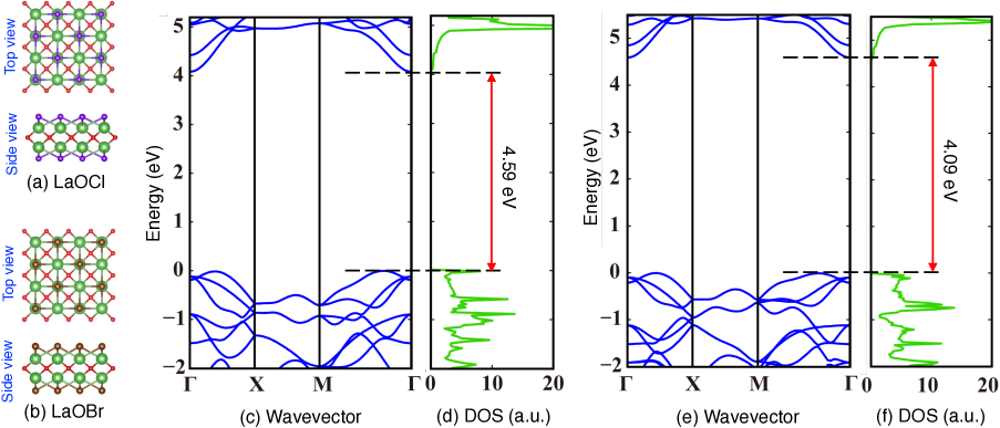
The lattice structure and the electronic band structures of LaO are shown in Fig. 1. Structurally, LaOX is a tetragonal lattice with a central oxygen layer sandwiched by La atoms. The La atoms are covered by an outer layer composed of halogen atoms [see Figs. 1(a) and (b)]. The lattice constants of LaOCl and LaOBr are Åand Å, respectively. The electronic band structure and density of states (DOS) of freestanding LaOCl [Figs. 1(c) and 1(d)] and LaOBr [Figs. 1(e) and 1(f)] suggests that an indirect band gap of 4.59 eV and 4.09 eV, respectively, which is consistent with the values reported in previous work [24] (see Table I for summary of key parameters of the structural and electronic properties of monolayer LaOCl, LaOBr, MoS2 and WS2). We note that as the band gap values are larger than 4.0 eV at the PBE level, LaOCl and LaOBr can be categorized as dielectric materials. Particularly for gate dielectric applications, previous machine-learning-based investigation has uncovered a semi-empirical expression for the intrinsic dielectric breakdown field strength [35], , where is the band gap of the dielectric material, and is the maximum phonon frequency. The large band gap values of LaOCL and LaOBr are thus beneficial for achieving high dielectric breakdown strength. We further note that as the constructed 2D/2D dielectric/semiconductor vdWH contains large number of atoms (i.e. 93 atoms in the supercell), PBE method, which underestimate the band gap as compared to the more computationally expensive HSE06 hybrid functional method (i.e. 5.83 eV and 5.68 eV, respectively, for LaOCl and LaOBr [24]), is employed in this work due to computational resource constraint. Nevertheless, the PBE calculation is expected to yield the same qualitative physics insights for 2D material vdWHs [36].
| Monolayer | (Å) | (eV) | (eV) | (eV) |
|---|---|---|---|---|
| LaOCl | 3.99 | -2.07 | -6.66 | 4.59 |
| LaOBr | 4.04 | -2.46 | -6.65 | 4.09 |
| MoS2 | 3.18 | -4.23 | -5.93 | 1.70 |
| WS2 | 3.18 | -3.84 | -5.68 | 1.84 |
| vdWH | (%) | (eV) | (Å) | (eV) | (eV) | (eV) | ||||
|---|---|---|---|---|---|---|---|---|---|---|
| LaOCl/MoS2 | 1.66 | -2.35 | 3.14 | -3.97 | -5.88 | 1.91 | 2.16 | 0.73 | 1.21 | 1.10 |
| LaOCl/WS2 | 1.66 | -2.49 | 3.18 | -3.68 | -5.69 | 2.01 | 1.77 | 0.98 | 0.80 | 1.41 |
| LaOBr/MoS2 | 0.78 | -2.38 | 3.21 | -4.18 | -5.85 | 1.67 | 1.77 | 0.62 | 1.10 | 0.85 |
| LaOBrWS2 | 0.78 | -2.38 | 3.26 | -3.76 | -5.68 | 1.92 | 1.38 | 0.87 | 0.74 | 1.15 |
For both LaOCl and LaOBR, the CBM is situated at the point while the VBM is situated along the - and the - directions. The CBM and VBM energies are -2.07 eV and -6.66 eV, respectively, for LaOCl and are -2.46 eV and -6.55 eV, respectively, for LaOBr, where vacuum level is defined as zero. Remarkably, the CBM and VBM energies of MoS2 (i.e. -4.23 eV and -5.93 eV, respectively) and WS2 (i.e. -3.84 eV and -5.68 eV, respectively) conveniently located around the middle portion of the band gap of both LaOCl and LaOBr, suggesting that sizable CBO and VBO can be achieved. Using the Anderson rule [37] which provides a simple estimation of the band offsets by aligning the vacuum level of two contacting materials [38], the magnitude of the CBO and VBO energies can be estimated as
| (1a) | |||
| (1b) |
respectively, where and are the CBM and VBM energies of the th monolayer ( for bilayer vdWH), respectively. Accordingly, the band offsets ranges from the lowest value of eV for LaOBr/MoS2 to the highest value of eV for LaOCl/MoS2. The sizable CBO and VBO estimated via Anderson rule provide a preliminary assurance on the feasibility of LaOCl and LaOBr as gate dielectrics to MoS2 and WS2 monolayers, which will be further verified via direct DFT calculations in the following sections.
| vdWH | (eV) | (e) | (eV) | (Å) | (eV) | (Å) |
|---|---|---|---|---|---|---|
| LaOCl/MoS2 | -0.03 | 0.05 | 5.28 | 1.92 | 3.37 | 1.69 |
| LaOCl/WS2 | -0.06 | 0.04 | 5.07 | 1.88 | 3.06 | 1.63 |
| LaOBr/MoS2 | 0.04 | 0.08 | 5.24 | 1.92 | 3.57 | 1.70 |
| LaOBrWS2 | 0.01 | 0.06 | 5.11 | 1.95 | 3.19 | 1.74 |
III.2 Structural and Electronic Properties of LaO/S2 Heterostructures
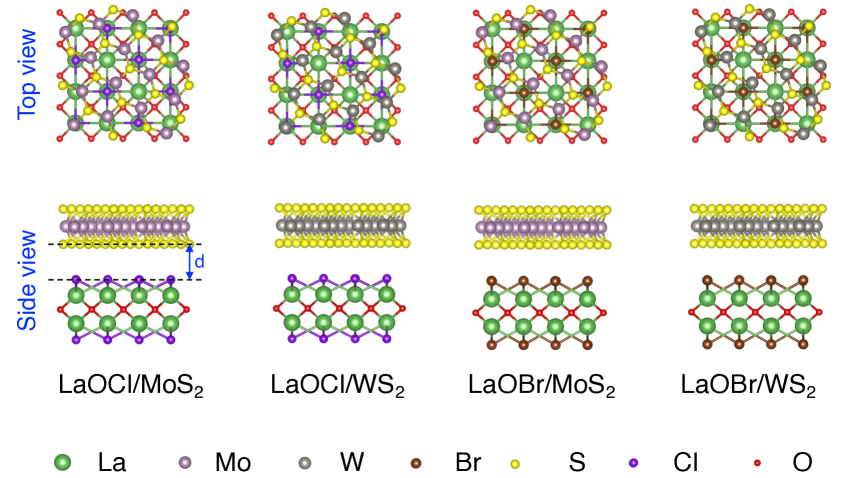
Four 2D/2D dielectric/semiconductors are constructed: (i) LaOCl/MoS2; (ii) LaOCl/WS2; (iii) LaOBr/MoS2; and (iv) LaOBr/WS2. The top and side views of the fully relaxed structures are shown in Fig. 2 (see Table 2 for a summary of the key parameters calculated for LaO/S2 heterostructures). Upon forming the heterostructure, a strain of 1.66% and 0.78% is evenly distributed among the two monolayers for LaOCl/S2 and LaOBr/S2 heterostructures, respectively, due to lattice mismatch. The interlayer distances of the heterostructures range between 3.1 Åto 3.4 Å, thus suggesting that the constituent monolayers are coupled weakly via van der Waals forces. The binding energy of the heterostructure can be calculated as [39]:
| (2) |
where , and are the total energy of the combined vdWH, LaO and S2, respectively. As summarized in Table II, all heterostructures have eV after full structural relaxation, hus confirming their energetic stability.
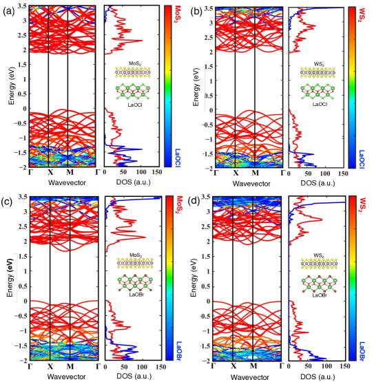
In Fig. 3, the electronic band structures and the DOS projected to the constituent monolayers are shown. The electronic bands of M2 and LaO are clearly can be clearly distinguished around the band edges, thus suggesting minimal hybridization of the two materials. The band gap of LaOCl/MoS2 and LaOCl/WS2 are 1.91 eV and 2.01 eV, respectively, which are slightly enhanced as compared to that of freestanding MoS2 and WS2 (i.e. 1.70 eV and 1.84 eV, respectively, due to the straining of the 2D semiconductors. For LaOBr/MoS2 and LaOBr/WS2 heterostructures, because of the smaller lattice mismatch of %, the band gap values are 1.67 eÍV and 1.92 eV, respectively, which are much closer to the freestanding monolayer band gap values. The CBO and VBO can be extracted from the DOS via
| (3a) | |||
| (3b) |
respectively. The band offsets obtained from direct DFT calculations ranges from eV for LaOBr/WS2 to eV for LaOCl/WS2 (see Table II). The band offsets obtained via direct DFT calculations are quantitatively different from those obtained via Anderson rule since DFT calculations explicitly capture the interlayer interactions between the two constituent monolayers [40]. Furthermore, the presence of strain due to lattice mismatch also modulates the band gap of both LaO and S2 monolayers. Particularly, LaOCl/MoS2 are found to be eV in both CBO and VBO. As MoS2 is a widely studied 2D semiconductors capable of achieving exceptionally low contact resistance [41] and strongly suppressed Fermi level pinning effect [42], the sizable CBO and VBO of LaOCl/MoS2 reveal LaOCl as an exceptional dielectric companion that can further enhance the device performance and reliability of 2D MoS2 nanoelectronic devices.
III.3 Interfacial Charge Transfer and Tunneling-Specific Interface Resistivity
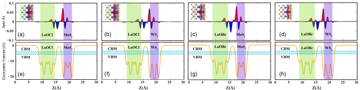
To further elucidate the interface properties of LaO/S2, we calculate the plane-averaged differential charge density () across the contact heterostrucures [Figs. 4(a) to 4(d)]. In general, electron is transferred from the LaO monolayer to the S2 monolayer due to the significantly lower electron affinity of S2. The differential charge density are smaller than 0.1 e/Åacross the heterostructure, suggesting that the interfacial charge transfer is negligible. Based on Bader charge analysis [34], the calcualted charge transfer between the monolayer is less than 0.1 e for all vdWHs (see Table 1). The ultralow interfacial charge transfer is also reflected in the plane-averaged electrostatic profile of the contact heterostructures [see Figs. 4(e) to 4(h)]. The interfacial dipole potential (), which arises due to electron accumulaton on one monolayer and electron depletion on the other monolayer, can be calculated as the vacumm level difference on both sides of the vdWH. We found that is typically in the order of eV for all LaO/S2 vdWHs, which is consistent with the overall low () observed in Figs. 4(a) to 4(d).
| vdWH | (cm 2) | (cm 2) | (Acm-2) | (Acm-2) | (Acm-2) | (Acm-2) |
|---|---|---|---|---|---|---|
| LaOCl/MoS2 | 1.62 | 0.47 | ||||
| LaOCl/WS2 | 1.35 | 0.37 | ||||
| LaOBr/MoS2 | 1.60 | 0.51 | ||||
| LaOBrWS2 | 1.67 | 0.50 |
A tunneling barrier (TB) is commonly formed across the van der Waals gap (vdWG) separating the two monolayers [43]. The height and width of the TB can be directly estimated from the plane-averaged electrostatic profiles of the vdWH. In metal/semiconductor contacts, the presence of TB in the vdWG substantially lowers the charge injection efficiency and is often more desirable to eliminate the vdW TB as much as possible. However, for gate dielectric applications in dielectric/semiconductor contact, vdW TB provide an additional mechanism, in addition to band offsets, to suppress the leakge current. Unlike metal/semiconductor contact in which the TB height and width are extracted based on the intersection of the Fermi level and the electrostatic potential profile, the Fermi level in dielectric/semiconductor contact cannot be straightforwardly defined as is material-and/or device-dependent [43]. Instead, we characterize the height and width by using the intersection of the CBM and VBM with the electrostatic profile [see Figs. 4(e) to 4(h)] since the electronic states around the CBM and VBM are dominantly responsible for carrier conduction in -type and -type device, respectively. The extracted TB heights and widths can be used to calculate the electron tunneling probability based on the WKB formalism [44],
| (4) |
where is the free electron mass, is the Planck constant, and represents the TB width and height, respectively. Here is an important quantity characterizing the charge injection efficiency across the vdWG since the ballistic tunneling current and the tunneling-specific interface resistivity across the vdWG are both directly related to [44]. The tunneling-specific interface resistivity can be calculated based on the Simmons tunneling diode model at low bias voltage [45],
| (5) |
Although is a quantity detrimental to charge injection efficiency for metal/semiconductor contact application, its presence in dielectric/semiconductor interface offers a mechanism unique to vdWHs for suppressing the leakage current. For LaO/S2 vdWHs, are found to be ranging from to cm2, which is comparable to other metal/semiconductor contacts [41, 46] (see Table IV).
III.4 Leakage Current: Interfacial Charge Injection and Interface Potential Barrier Tunneling
To assess the capability of LaO as gate dielectrics to 2D TMDC, we calculate the leakage current of LaO/S2 using the DFT-calculated band offset values. The leakage current is dominantly contributed by transport mechanisms [47, 48]: (i) semiclassical overbarrier thermionic emission (TE); and (ii) quantum mechanical field-induced emission (FE). Based on the Murphy-Good model [29], the leakage current density is
| (6) | ||||
where the subscript for leakage current flowing in the conduction band and the valance band, respectively, is the Boltzmann constant, is the temperature, is the applied field, is the effective constant potential of electrons in the metal contact and can be taken as for most metals, , , is an elliptical function arising from image-charge effect [29] and is the out-of-plane static dielectric constant of the dielectric layer. The first and second term in the right-hand side of Eq. (6) corresponds to the underbarrier quantum mechanical field-induced tunneling and the overbarrier semiclassical thermionic emission, respectively. We assume a planar diode geometry, i.e. , where the tunneling distance is and the potential difference across the dielectric is V based on the IRDS specifications of supply power voltage and saturation voltage V [24, 49]. Here is the free-electron mass and is the effective electron or hole masses of LaO for leakage current conduction mediated by conduction band or by valance band, respectively. Based on previous DFT calculations [24], the electron and hole masses of LaOCl (LaOBr) is 1.125 (2.251 ) and 1.475 (1.180 ), respectively. The thickness of LaOCl and LaOBr monolayer is Åand Å, respectively [24]. The tunneling distance is then estimated as where we assume that the LaO monolayer forms van der Waals contacts at both of its top and bottom surfaces with a typical van der Waals gap distance of Å.
Equation (6) can be simplified into a ‘tunneling’ and a ‘thermionic’ component to yield a simplified leakage current formula commonly used in the literature [24, 28], i.e. , where
| (7a) | |||
| (7b) |
In Table IV, we calculate the leakage current using both the Murphy-Good and the simplified models. In general, the simplified model underestimates the leakage current. The underestimation can reach about 3 orders of magnitude (i.e. CBO leakage currents of LaOCl/WS2 and LaOBr/WS2, and VBO leakage currents of LaOCl/MoS2 and LaOCl/WS2), thus highlighting the importance of using Murphy-Good model to obtain a more accurate estimation of the leakage currents. The CBO leakage currents of LaOCl/WS2 and LaOBr/WS2 are higher than the Acm-2 threshold proposed in [25], thus suggesting that LaO may not be suitable for NMOS configurations in WS2-based devices. Similarly, the sizable VBO leakage current of LaOBr/MoS2 reveals the incompatibility for PMOS application. Nevertheless, the CBO and VBO leakge currents of LaOCl/MoS2 are both in the orders of 10-7 and Acm-2, respectively, which are significantly lower than the Acm-2 threshold leakage current threshold. LaOCl/MoS2 is thus a versatile dielectric/semiconductor combinations that are simultaneously compatible for both NMOS and PMOS operations, while LaO/WS2 combinations are generally compatible with PMOS operations. If we relax the leakage current limit from Acm-2 [25] to the IRDS 2020 standard [49] of 0.145 Acm-2 for a device of 28 nm pitch, 18 nm long gate, and an effective gate of 107 nm as proposed in [28], then both LaOCl/MoS2 and LaOBr/MoS2 are simultaneously compatible with NMOS and PMOS device configurations.
IV Conclusion
In summary, we performed DFT calcualtions to investigate the interfacial properties of dielectric/semiconductor van der Waals heterostructures composed of LaO ( Cl, Br) and S2 (Mo, W) monolayers. We found that the contact heterostructures exhibit negligible hybridization and interfacial charge transfer, thus completely preserving the electronic properties of the contacted S2 TMDC monolayers. Importantly, the conduction and valance bands edges exhibit sizable band offsets in LaOCl/MoS2 contact, thus suggesting its compatibility for both PMOS and NMOS device configurations, while LaO/Br are compatible with PMOS device configuration. Together with the previously predicted exceptional out-of-plane static dielectric constants of LaO monolayers, our results suggest that LaOCl and LaOBr are excellent gate dielectric layered materials for MoS2 and WS2. This work provides theoretical foundation and interface physics insights that are useful for the design of novel 2D semiconductor devices utilizing atomically thin LaO as gate dielectrics, and shall provide a practical motivation for the experimental searches of LaOCl and LaOBr monolayers.
Acknowledgement
This work is supported by Singapore Ministry of Education (MOE) Academic Research Fund (AcRF) Tier 2 (MOE-T2EP50221-0019). Z.J. and L.K. Ang are supported by ASTAR AME IRG (A2083c0057)
References
- [1] S. Wang, X. Liu, and P. Zhou. “The road for 2d semiconductors in the silicon age,” Adv. Mater., to be published. DOI: 10.1002/adma.202106886.
- [2] S. Haastrup, M. Strange, M. Pandey, T. Deilmann, P. S. Schmidt, N. F. Hinsche, T. N. Gjerding, D. Torelli, T. M. Larsen, A. C. Riis-Jensen, J. Gath, K. W. Jacobsen, J. J. Mortensen, T. Olsen, and K. S. Thygesen. “The computational 2d materials database: high-throughput modeling and discovery of atomically thin crystals,” 2D Mater., vol. 5, no. 4, pp. 042002, Sep. 2018. DOI: 10.1088/2053-1583/aacfc1.
- [3] M. N. Gjerding, A. Taghizadeh, A. Rasmussen, S. Ali, F. Bertoldo, T. Deilmann, N. R. Knøsgaard, M. Kruse, A. H. Larsen, S. Manti, T. G. Pedersen, U. Petralanda, T. Skovhus, M. K. Svendsen, J. J. Mortensen, T. Olsen, and K. S. Thygesen. “Recent progress of the computational 2d materials database (c2db),” 2D Mater., vol. 8 no., pp. 044002, Jul. 2021. DOI: 10.1088/2053-1583/ac1059.
- [4] S. M. Young and C. L. Kane. “Dirac semimetals in two dimensions,” Phys. Rev. Lett., vol. 115, no. 12, pp. 126803, Sep. 2015. DOI: 10.1103/PhysRevLett.115.126803.
- [5] M. Gu, S. A. Wolf, and J. Lu. “Two-dimensional mott insulators in srvo3 ultrathin films.” Adv. Mater. Interfaces, vol. 1, no. 7, pp. 1300126, Jun. 2014. DOI: 10.1002/admi.201300126.
- [6] Z. F. Wang, B. Liu, and W. Zhu. “Hourglass fermion in two-dimensional material,” Phys. Rev. Lett., vol. 123, no. 12, no. pp. 126403, Sep 2019. DOI: 10.1103/PhysRevLett.123.126403.
- [7] H. Wang, L. Yu, Y.-H. Lee, Y. Shi, A. Hsu, M. L. Chin, L.-J. Li, M. Dubey, J. Kong, and T. Palacios. “Integrated circuits based on bilayer mos2 transistors,” Nano Lett., vol. 12, no. 9, pp. 4674–4680, Aug. 2012. DOI: 10.1021/nl302015v.
- [8] A. Pal, S. Zhang, T. Chavan, K. Agashiwala, C.-H. Yeh, W. Cao, and K. Banerjee, “Quantum-engineered devices based on 2D materials for next-generation information processing and storage”, Adv. Mater., to be published. DOI: 10.1002/adma.202109894.
- [9] M. E. Pam, S. Li, T. Su, Y.-C. Chien, Y. Li, Y. S. Ang, and K.-W. Ang. “Interface-modulated resistive switching in mo-irradiated res2 for neuromorphic computing,” Adv. Mater., vol. 34, no. 30, 2202722, Jul. 2022. DOI: 10.1002/adma.202202722.
- [10] Y. Lv, W. Qin, C. Wang, L. Liao, and X. Liu. “Recent advances in low-dimensional heterojunction-based tunnel field effect transistors,” Adv. Electron. Mater., vol. 5, no. 1, pp. 1800569, Jan. 2019. DOI: 10.1002/aelm.201800569.
- [11] Y. S. Ang, S. A. Yang, C. Zhang, Z. Ma, and L. K. Ang. “Valleytronics in merging dirac cones: All-electric-controlled valley filter, valve, and universal reversible logic gate,” Phys. Rev. B, vol. 96, no. 24, pp. 245410, Dec. 2017. DOI: 10.1103/PhysRevB.96.245410.
- [12] A. R. Wright, X. G. Xu, J. C. Cao, and C. Zhang. “Strong nonlinear optical response of graphene in the terahertz regime,” Appl. Phys. Lett., vol. 95, no. 7, pp. 072101, 2009. DOI: 10.1063/1.3205115.
- [13] Y. S. Ang, S. Sultan, and C. Zhang. “Nonlinear optical spectrum of bilayer graphene in the terahertz regime,” Appl, Phys. Lett., vol. 97, no. 24, pp. 243110, 2010. DOI: 10.1063/1.3527934.
- [14] G. Wang, J. Chang, W. Tang, W. Xie, and Y. S. Ang. “2D materials and heterostructures for photocatalytic water-splitting: a theoretical perspective, ” J. Phys. D: Appl. Phys., vol. 55, no. 29, pp. 293002, Mar. 2022. DOI: 10.1088/1361-6463/ac5771.
- [15] Z. Zhang, B. Cheng, J. Lim, A. Gao, L. Lyu, T. Cao, S. Wang, Z.-A. Li, Q. Wu, L. K. Ang, Y. S. Ang, S.-J. Liang, and F. Miao. “Approaching intrinsic threshold breakdown voltage and ultra-high gain in graphite/inse schottky photodetector,” Advanced Materials, to be published. DOI: 10.1002/adma.202206196.
- [16] F. Palumbo, C. Wen, S. Lombardo, S. Pazos, F. Aguirre, M. Eizenberg, F. Hui, and M. Lanza. “A review on dielectric breakdown in thin dielectrics: Silicon dioxide, high-k, and layered dielectrics,” Adv. Functl. Mater., vol. 30, no. 18, pp. 1900657, May. 2020. DOI: 10.1002/adfm.201900657.
- [17] A. Ranjan, N. Raghavan, M. Holwill, K. Watanabe, T. Taniguchi, K. S. Novoselov, K. L. Pey, and S. J. O’Shea. “Dielectric breakdown in single-crystal hexagonal boron nitride,” ACS Appl. Electron. Mater., vol. 3, no. 8, pp. 3547–3554, Aug. 2021. DOI: 10.1021/acsaelm.1c00469.
- [18] F. Mahvash, E. Paradis, D. Drouin, T. Szkopek, and M. Siaj. “Space-charge limited transport in large-area monolayer hexagonal boron nitride,” Nano Lett., vol. 15, no. 4, pp. 2263–2268, Mar. 2015. DOI. 10.1021/nl504197c.
- [19] Y. S. Ang, M. Zubair, and L. K. Ang. “Relativistic space-charge-limited current for massive dirac fermions,” Phys. Rev. B, vol. 95, no. 16, pp. 165409, Apr. 2017. DOI: 10.1103/PhysRevB.95.165409.
- [20] L. Britnell, R. V. Gorbachev, R. Jalil, B. D. Belle, F. Schedin, M. I. Katsnelson, L. Eaves, S. V. Morozov, A. S. Mayorov, N. M. R. Peres, A. H. Castro Neto, J. Leist, A. K. Geim, L. A. Ponomarenko, and K. S. Novoselov. “Electron tunneling through ultrathin boron nitride crystalline barriers,” Nano Lett., vol. 12, no. 3, pp. 1707–1710, Mar. 2012. DOI: 10.1021/nl3002205
- [21] Y. Hattori, T. Taniguchi, K. Watanabe, and K. Nagashio. “Layer-by-layer dielectric breakdown of hexagonal boron nitride, ” ACS Nano, vol. 9, no. 1, pp. 916–921, Dec. 2015. DOI: 10.1021/nn506645q.
- [22] A. R., F. M. P., N. R., S. J. O’Shea, K. Shubhakar, P. Pavan, A. Padovani, L. Larcher, and K. L. Pey. “Random telegraph noise in 2d hexagonal boron nitride dielectric films,” Appl. Phys. Lett., vol. 112, no. 13, pp. 133505, Mar. 2018. DOI: 10.1063/1.5022040.
- [23] A. Laturia, M. L. Van de Put, and W. G. Vandenberghe. “Dielectric properties of hexagonal boron nitride and transition metal dichalcogenides: from monolayer to bulk, ” npj 2D Mater. Appl., vol. 2, pp. 6, Mar. 2018. DOI: 10.1038/s41699-018-0050-x.
- [24] M. R. Osanloo, M. L. van de Put, A. Saadat, and W. G. Vandenberghe. “Identification of two-dimensional layered dielectrics from first principles,” Nat. Commun., vol. 12, pp. 5051, 2021. DOI: 10.1038/s41467-021-25310-2.
- [25] Y. Y. Illarionov, T. Knobloch, M. Jech, M. Lanza, D. Akinwande, M. I. Vexler, T. M., M. C. Lemme, G. Fiori, F. Schwierz, and T. Grasser. “Insulators for 2d nanoelectronics: the gap to bridge, ” Nat. Commun., vol. 11, pp. 3385, Jul. 2020. DOI: 10.1038/s41467-020-16640-8.
- [26] S.-J. Liang, B. Cheng, X. Cui, and F. Miao. “Van der waals heterostructures for high-performance device applications: Challenges and opportunities, ” Adv. Mater., vol. 32, no. 27, pp. 1903800, Jul. 2020. DOI: 10.1002/adma.201903800.
- [27] L. Teitz and M. C. Toroker. “Theoretical investigation of dielectric materials for two-dimensional field-effect transistors, ” Adv. Functl. Mater., vol. 30, no. 18, pp. 1808544, May. 2020. DOI: 10.1002/adfm.201808544.
- [28] M. R. Osanloo, A. Saadat, M. L. Van de Put, A. Laturia, and W. G. Vandenberghe. “Transition-metal nitride halide dielectrics for transition-metal dichalcogenide transistors, ” Nanoscale, vol. 14, 157–165, Jan. 2022. DOI: 10.1039/D1NR05250K.
- [29] E. L. Murphy and R. H. Good. “Thermionic emission, field emission, and the transition region,” Phys. Rev., vol. 102, no. 6, pp. 1464–1473, Jun. 1956. DOI: 10.1103/PhysRev.102.1464.
- [30] G. Kresse and J. Furthmüller. “Efficient iterative schemes for ab initio total-energy calculations using a plane-wave basis set, ” Phys. Rev. B, vol. 54, no. 16, pp. 11169–11186, Oct. 1996. DOI: 10.1103/PhysRevB.54.11169.
- [31] P. E. Blöchl. “Projector augmented-wave method, ” Phys. Rev. B, vol. 50, no. 24, pp. 17953–17979, Dec. 1994. DOI: 10.1103/PhysRevB.50.17953.
- [32] J. P. Perdew, K. Burke, and M. Ernzerhof. “Generalized gradient approximation made simple, ” Phys. Rev. Lett., vol. 77, no. 18, pp. 3865–3868, Oct. 1996. DOI: 10.1103/PhysRevLett.77.3865.
- [33] S. Grimme, J. Antony, S. Ehrlich, and H. Krieg. “A consistent and accurate ab initio parametrization of density functional dispersion correction (dft-d) for the 94 elements h-pu, ” J. of Chem. Phys., vol. 132, no. 15, pp. 154104, Apr. 2010. DOI: 10.1063/1.3382344.
- [34] G. Henkelman, A. Arnaldsson, and H. Jónsson. “A fast and robust algorithm for bader decomposition of charge density, ” Comput. Mater. Sci., vol. 36, no. 3, pp. 354–360, Jun. 2006. DOI: 10.1016/j.commatsci.2005.04.010.
- [35] C. Kim, G. Pilania, and R. Ramprasad. “From organized high-throughput data to phenomenological theory using machine learning: The example of dielectric breakdown, ” Chem. Mater., vol. 28, no. 5, pp. 1304–1311, Feb. 2016. DOI: 10.1021/acs.chemmater.5b04109.
- [36] R. Besse, J. F. R. V. Silveira, Z. Jiang, D. West, S. Zhang, and J. L. F. Da Silva. “Beyond the anderson rule: importance of interfacial dipole and hybridization in van der waals heterostructures, ” 2D Mater., vol. 8, no. 4, pp. 041002, Aug. 2021. DOI: 10.1088/2053-1583/ac1902.
- [37] K. Xu, Y. Xu, H. Zhang, B. Peng, H. Shao, G. Ni, J. Li, M. Yao, H. Lu, H. Zhu, and C. M. Soukoulis. “The role of anderson’s rule in determining electronic, optical and transport properties of transition metal dichalcogenide heterostructures, ” Phys. Chem. Chem. Phys., vol. 20, no. 48, pp. 30351–30364, Nov. 2018. DOI: 10.1039/C8CP05522J.
- [38] F. H. Davies, C. J. Price, N. T. Taylor, S. G. Davies, and S. P. Hepplestone. “Band alignment of transition metal dichalcogenide heterostructures, ” Phys. Rev. B, vo. 103, no. 4, pp.045417, Jan. 2021. DOI: 10.1103/PhysRevB.103.045417.
- [39] B. Amin, N. Singh, and U. Schwingenschlögl. “Heterostructures of transition metal dichalcogenides, ” Phys. Rev. B, vol. 92, no. 7, pp. 075439, Aug. 2015. DOI: 10.1103/PhysRevB.92.075439.
- [40] Y. Si, H.-Y. Wu, K. Yang, J.-C. Lian, T. Huang, W.-Q. Huang, W.-Y. Hu, and G.-F. Huang. “High-throughput computational design for 2d van der waals functional heterostructures: Fragility of anderson’s rule and beyond, ” Appl. Phys. Lett., vol. 119, no. 4, pp. 043102, Jul. 2021. DOI: 10.1063/5.0058156.
- [41] P.-C. Shen, C. Su, Y. Lin, A.-S. Chou, C.-C. Cheng, J.-H. Park, M.-H. Chiu, A.-Y. Lu, H.-L. Tang, M. M. Tavakoli, G. Pitner, X. Ji, Z. Cai, N. Mao, J. Wang, V. Tung, J. Li, J. Bokor, A. Zettl, C.-I Wu, T. Palacios, L.-J. Li, and J. Kong. “Ultralow contact resistance between semimetal and monolayer semiconductors, ” Nature, vol. 593, pp. 211–217, May. 2021. DOI: 10.1038/s41586-021-03472-9.
- [42] Y. Liu, J. Guo, E. Zhu, L. Liao, S.-J. Lee, M. Ding, I. Shakir, V. Gambin, Y. Huang, and X. Duan. “Approaching the schottky–mott limit in van der waals metal–semiconductor junctions, ” Nature, vol. 557, pp. 696–700, May. 2018. DOI: 10.1038/s41586-018-0129-8.
- [43] J. Kang, W. Liu, D. Sarkar, D. Jena, and K. Banerjee. “Computational study of metal contacts to monolayer transition-metal dichalcogenide semiconductors, ” Phys. Rev. X, vol. 4, no. 3, pp. 031005, Jul. 2014. DOI: 10.1103/PhysRevX.4.031005.
- [44] L. Cao, X. Deng, Z. Tang, G. Zhou, and Y. S. Ang. “Designing high-efficiency metal and semimetal contacts to two-dimensional semiconductor -gese, ” Appl. Phys. Lett., vol. 121, no. 11, pp. 113104, Sep. 2022. DOI: 10.1063/5.0117670.
- [45] J. G. Simmons. “Generalized formula for the electric tunnel effect between similar electrodes separated by a thin insulating film, ” J. Appl. Phys., vol. 34, no. 6, pp. 1793–1803, Jun. 1963. DOI: 10.1063/1.1702682
- [46] Q. Wang, L. Cao, S.-J. Liang, W. Wu, G. Wang, C. H. Lee, W. L. Ong, H. Y. Yang, L. K. Ang, S. A. Yang, and Y. S. Ang. “Efficient ohmic contacts and built-in atomic sublayer protection in mosi2n4 and wsi2n4 monolayers, ” npj 2D Mater. Appl., no. 5, pp. 71, Aug. 2021. DOI: 10.1038/s41699-021-00251-y.
- [47] Y. S. Ang, L. Cao, and L. K. Ang. “Physics of electron emission and injection in two-dimensional materials: Theory and simulation, ” InfoMat, vol. 3, no. 5, pp. 502–535, May. 2021. DOI: 10.1002/inf2.12168.
- [48] Y. S. Ang, H. Y. Yang, and L. K. Ang, “Universal scaling laws in Schottky heterostructures based on two-dimensional materials, ” Phys. Rev. Lett., vol. 121, no. 5, pp. 056802, Aug. 2018. DOI: 10.1103/PhysRevLett.121.056802.
- [49] International Roadmap Committee, International Roadmap for Devices and Systems 2022 Edition. [Online]. Available: https://irds.ieee.org/editions/2022, Accessed on: Oct. 5, 2022