Chirality-induced intrinsic charge rectification in a tellurium-based field-effect transistor
Abstract
We report gate-induced enhancement of intrinsic charge rectification without p-n junctions in chiral semiconductor Te under magnetic field . As gating shifts the chemical potential to the valence band maximum of Te, the charge rectification efficiency is enhanced hundredfold. By integrating model calculations, we attribute the charge rectification to the -induced asymmetry of the chiral band structure. We also show that the carrier density subject to this asymmetry is augmented by a saddle-point structure near the valence band maximum, which further enhances the gate-tunable charge rectification together with its improved switchability and thermal robustness.
Introduction.— Chiral crystal structure is characterized by breaking of mirror and inversion symmetries. This characterization carries over to momentum space and demands that spin degeneracy of the electronic band be lifted by spin-orbit interaction (SOI). As a result, spin-momentum locking emerges and enables one to electrically control electron spins even in nonmagnetic materials. This property in noncentrosymmetric materials has attracted attention in spintronics research [1]. Interestingly, the spin can be coupled parallel to the momentum in chiral crystals via SOI [2, 3, 4, 5, 6], which has only recently been verified conclusively [7, 8]. The resulting spin-momentum locking is hedgehoglike in momentum space and unique to chiral crystals. The spin-momentum locking is described by chiral SOI, called Weyl-type SOI, in the form of with being SOI strengths ().
Chiral materials have been gaining renewed attention as spin polarizers since the discovery of chirality-induced spin selectivity (CISS) in chiral molecules [9, 10, 11, 12]. Recent extension of CISS from molecules to inorganic metals CrNb3S6 and disilicides suggested micrometer-scale spin-propagation lengths by nonlocal transport measurement [13, 14] and a high spin-polarization rate by SQUID magnetometry [15]. Additionally, CISS has been integrated into organic-inorganic hybrid materials [16, 17, 18, 19], in which regularly structured chiral molecules act as multiple spin filters. These findings could be steps forward to future spintronics, although the mechanism remains to be clarified [12]. We note that charge transport phenomena related with Weyl-type SOI follow the same selection rule as CISS [13, 14]. This makes it impossible to distinguish these two effects by symmetry consideration. A criterion for CISS appears to lie in the high efficiency of charge-to-spin conversion beyond conventional spintronic effects. Therefore, it is critical to explore a quantitative approach to transport phenomena caused by spin-momentum locking in chiral crystals.
Elemental Te is the simplest chiral crystal with strong Weyl-type SOI. Te was recently shown to host a hedgehoglike spin texture near the highly symmetrical points in momentum space by angle-resolved photoemission spectroscopy [7, 8]. Additionally, charge rectification caused by spin-momentum locking without p-n junctions [20, 21] has been reported both for bulk crystals [22] and for nanowires [23]. These studies encouraged us to explore a quantitative approach to charge rectification caused by spin-momentum locking in Te alongside its possible relation with CISS.
In this Letter, we achieve giant charge rectification caused by spin-momentum locking of a p-type thin-film transistor (TFT) of elemental Te. A high on/off current ratio of enables us to reach the valence band maximum (VBM) of Te and to investigate charge transport caused by spin-momentum locking in a special band structure. As gating shifts the chemical potential towards the VBM, the charge rectification efficiency is enhanced by 100, which far exceeds a factor of 6 reported for Te nanowires [23]. By integrating TFT characterization, we also reveal that the enhancement starts when the chemical potential approaches a saddle point slightly below the VBM. Our observations are rationalized by the semiclassical Boltzmann transport theory which takes into account chiral spin-momentum locking under external magnetic field. The excellent correspondence indicates that the charge rectification results from the magnetic-field-induced asymmetry of the chiral band structure. The calculation also shows that near-VBM hole carriers contribute dominantly to this effect. We suggest that the augmented density of such carriers in the saddle-point band structure improves the on/off ratio of the charge rectification, and makes the rectification robust against thermal fluctuation.
Spin-split energy bands of Te.— Elemental Te is a typical chiral semiconductor and the spin-split energy bands have been studied comprehensively [5, 24, 25]. The chirality is known to determine the polarity of many properties, including spin-momentum locking [7, 8], current-induced bulk magnetization [26, 27, 28, 29, 30] possibly protected by the emergent symmetry [31], optical activity [32, 33, 34, 35], second-harmonic generation [36], and diffraction with circularly polarized x rays [37]. In elemental Te, the atoms are covalently bound to form spiral chains along the axis [Fig. 1(a)]. These chains are bound together by van der Waals force in accordance with an enantiomorphic space group, either or . The anisotropic chemical bonding alongside strong SOI yields anisotropic spin textures in momentum space near the H and H’ points in the Brillouin zone [Fig. 1(b)]. As a result, the two upper branches of the valence band near those points consist mainly of and with being the component of total angular momentum of . Hybridization between these two states yields an energy gap of eV together with a saddle point near the VBM. The top branch of the valence band can be described by the effective Hamiltonian given by [23]
| (1) |
where represent deviations of from the -point. corresponds to the enantiomorphic space group and the last two terms proportional to represent Weyl-type SOIs. The parameters were set to those values in Ref. 23. The higher energy eigenstate of is the valence energy band, visualized in Figs. 1(c) and 1(d). We stress that previous experiments were susceptible to natural hole doping by Te vacancies [23] and failed to probe charge rectification in the vicinity of the VBM.
Experimental details.— Thin-film crystals of Te were prepared, washed, and laminated on heavily doped Si substrates covered with a SiO2 dielectric layer [Fig. 1(e)], following a procedure in Ref. 38. Te crystals are known to form millimeter-scale monodomains with one handedness [22, 7] and this monodomain formation carries over to thin-film crystals obtained by the same crystal growth method as ours [23]. Therefore, our Te-based TFT was also expected to be of one handedness, although we did not identify the space group of the Te thin-film crystal. Contact patterns were defined by standard photolithography and the contacts were made by depositing Au through a magnetron sputtering method. For TFT characterization [dc measurement in Fig. 1(f)], we took transfer curves by sourcing a drain voltage along the screw axis and measuring a drain current along the same axis. For charge rectification measurement [lock-in measurement in Fig. 1(f)], we employed phase-sensitive detection of longitudinal voltage in a physical property measurement system (Quantum Design). An alternating current was sourced with the frequency = 37.14 Hz and the amplitude nA. Voltages at first and second harmonics of were detected by lock-in amplifiers. The longitudinal voltages along the screw axis were measured while external magnetic field was applied along the same direction. For high-accuracy phase-sensitive detection, the lowest system temperature was limited to 20 K, below which a high sample resistance hindered high-accuracy measurement.
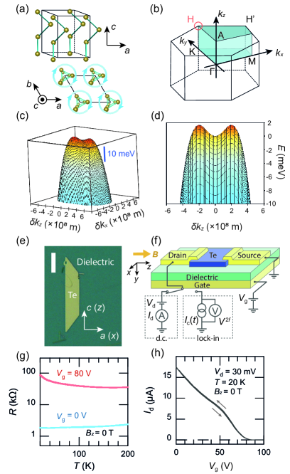
TFT Characterization.— In Fig. 1(g), we show the temperature dependence of the longitudinal resistance along the axis, measured at the fundamental frequency. When the gate voltage was set to 0 V, decreased with decreasing . The metallic conduction indicates that the Te crystal was naturally doped. When was set to +80 V, however, increased with decreasing and exhibited a semiconducting property. The result shows that the chemical potential was such that valence band states were almost filled up by applying , which changed charge conduction from metallic to semiconducting. Because this change took place at positive , we confirmed that our Te film was p doped and that was located in the vicinity of the VBM. The proximity of to the VBM is also supported by the dependence of the drain current . In Fig. 1(h), we show the transfer curve taken at 20 K. As is increased from 0 V, decreases and finally becomes indiscernible above V. The drain-current on/off ratio is , which is one of the best values reported for p-type Te TFT devices; Te crystals are subject to natural hole doping and do not always exhibit such a high on/off ratio. The excellent TFT property enables us to selectively populate near-VBM hole carriers and to investigate charge transport conveyed by those hole carriers in the presence of spin-momentum locking.
Charge rectification.— Having checked near-VBM charge conduction, we turn to charge rectification [20, 21] in the relevant energy range. Subsequently, we discuss charge rectification in the presence of a uniaxially large Weyl-type SOI, for example, , where distinguish left- and right-handed crystals. This SOI represents breaking of inversion and mirror symmetries, namely chirality. As a result, electrical resistivity has a bilinear correction with respect to the electric current density and the magnetic field . is given by
| (2) |
where is the resistivity at zero magnetic fields. This term represents charge rectification and the coefficient tensor describes the strength as well as the symmetry-adapted selection rule of the charge rectification. due to the anisotropic Weyl-type SOI is finite when and are applied along the direction. An approximate selection rule was demonstrated for hole transport in Te nanowires [23], probably because of the highly anisotropic Weyl-type SOI in the valence band. is related with chirality via and the tendency of Te to monodomain formation with one handedness is important to detect .
In the present setup [see also Fig. 1(f)], appears in an electric field at the second harmonic of , , where is a detected voltage at the second harmonic of , and is a distance between the detection electrodes. is given by [39]
| (3) |
where is the resistivity at the first harmonic of . , ( a cross-sectional area in the plane), and are all assumed to be along the screw axis ( axis), considering the anisotropic Weyl-type SOI.
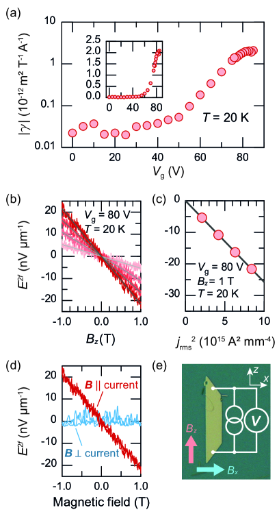
In Fig. 2(a), we show the dependence of at 20 K. The corresponding and dependences of are shown in Figs. 2(b) and 2(c), both of which are consistent with Eq. (3). As is increased from 0 V to 50 V, increases gradually by a factor of 2. However, upon a further increase of , increases exponentially and exhibits a drastic enhancement. As a result, at V is one hundred times larger than at V. This controllable enhancement is the greatest of three-dimensional normal conductors, being second to noncentrosymmetric superconductors [40]. Additionally, the chiral selection rule of is supported by the magnetic-field-direction dependence of as shown in Fig. 2(d). When was applied along the axis [see also Fig. 2(e)], a magnetic-field-linear signal was undetectable. If charge rectification resulted from inversion symmetry breaking by along the axis, would be greatest with axis and satisfy a selection rule of polar systems [41]. Since such a polar selection rule is absent in Fig. 2(d), -driven inversion symmetry breaking can be ignored in the present measurement. Instead, our results indicate that the -dependent originates directly from the chiral band structure of Te.

The enhancement of near the band edge is reminiscent of that of the polar semiconductor BiTeBr [41], although the value of can be one order of magnitude larger in this study. The charge rectification in BiTeBr was attributed to -induced asymmetry of the electronic band via the Zeeman effect alongside its polar atomic arrangement. Therefore, we calculate , denoted by to stress its microscopic nature, under the assumption that hole carriers are subject to the Zeeman interaction, , as well as Weyl-type SOI (see also Eq. 1). Here and are the effective g-factor and the Bohr magneton, respectively. According to Ref. 41, is given by
| (4) |
where and are first- and second-order electrical conductivities with respect to an external electric field, respectively. It should be noted that this formalism is independent of a relaxation time if is assumed to be constant. Therefore, we calculated by Boltzmann transport theory with a constant , using the valence band of the total Hamiltonian . and were taken into account by the Fermi-Dirac distribution function of hole carriers. In calculating , we assumed a two-dimensional limit by setting to 0 [41], because was applied along the axis to confine hole carriers in the plane [38].
In Figs. 3(a) and 3(b), we show the calculated dependences of obtained at K. is linear and vanishes at zero fields, consistent with our second-harmonic voltage measurements. Interestingly, as is increased towards the VBM at meV, increases and exhibits a peak structure [Fig. 3(c)] despite the monotonically decreasing [Fig. 3(d)]. When is above the VBM energy, , the major dependences of stem from the Boltzmann statistics through ( the Boltzmann constant); therefore, is enhanced exponentially with the corresponding threshold via , as shown in Fig. 3(e). The exponential enhancement with the characteristic threshold reproduces the -dependent . This demonstrates that near-VBM carriers dominate charge rectification due to the -induced band asymmetry [see also the inset to Fig. 3(e)] and that selectively populating those carriers results in efficient charge rectification.
We recall that the density of states (DOS) near the VBM is augmented by the saddle-point structure [42, 43, 44] [see also Fig. 1(c)], which is absent in noncentrosymmetric semiconductors studied previously. Such a DOS contributes to the characteristic peak structures of in Fig. 3(c), thereby further enhancing . We also suggest that anomalies near the saddle-point structure are more pronounced in experiments than in calculations [compare Figs. 1(h) and 2(a) with Figs. 3(d) and 3(e), respectively]. This indicates that the actual DOS in the saddle-point structure is larger than expected from possibly thanks to higher-order corrections to [25]. We argue that such a special band structure improves gate switchability of around V.
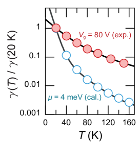
In Fig. 4, we compare the dependence of with our calculation in which a finite temperature effect was considered via the Fermi-Dirac statistics of hole carriers. We ignored the dependence of and set to 4 meV in calculation. As is increased from 20 K to 150 K, the experimental at V ( meV at 20 K) decreases monotonically. The dependence is reproduced qualitatively by the calculation, as shown in Fig. 4. This means that is due mainly to near-VBM hole carriers and shows that a decreasing ratio of such carriers to the total carrier density is responsible for the decreasing .
Interestingly, decreases less rapidly and is more robust against thermal fluctuation than the calculated . Several mechanisms can be responsible for the thermal robustness. In one scenario, the result can be attributed to a greater carrier density near the saddle point than expected and likewise the -tunable . Such carriers can contribute to across a wider energy range, thus making less dependent. Another scenario is a -dependent . In -doped semiconductors, shifts upwards with increasing , which helps to selectively populate near-VBM hole carriers. The last scenario is the relevance of chirality-induced spin selectivity (CISS), which intensifies with increasing [12]. Although CISS-based charge rectification has not been discussed in literature, this problem setting would be worth consideration. We note that CISS-induced magnetoresistance (MR) with ferromagnetic electrodes can reach tens of percents [12], which originates from spin-dependent interfacial resistance change. This experimental technique was not adopted in the present study; therefore, it is difficult to compare the charge rectification efficiency with previous MR values. Interfacial MR measurement with ferromagnetic electrodes is an important future study to clarify the possible coexistence of CISS in the present system. Such a MR device may also provide a systematic approach for investigating spin-dependent current–voltage characteristics of CISS without being plagued by the delicate nature of chiral molecular devices.
Summary.— We have demonstrated highly gate-tunable charge rectification caused by spin-momentum locking of a field-effect transistor of elemental Te. The charge rectification follows a chiral selection rule and its efficiency is gate variable by two orders of magnitude on demand. The correspondence with calculations shows that the chiral rectification stems from a concerted effect of Weyl-type spin-orbit interaction and Zeeman interaction with magnetic field. We expect that Te-based field-effect transistors provide ideal platforms for exploring chirality-induced nonreciprocal phenomena, including CISS.
Acknowledgements.
We thank E. Saitoh for a discussion on the saddle-point structure of elemental Te. We also thank T. Sato for experimental assistance. We are grateful to the Equipment Development Center (the Institute for Molecular Science) for custom-made equipment. This work was supported by Grant-in-Aid for Scientific Research (A) (Grant No. 19H00891) and for Challenging Research (Exploratory) (Grants No. 20K20903 and No. 22K18695) from JSPS KAKENHI, Japan as well as PRESTO “Topological Materials Science for Creation of Innovative Functions” (Grant No. JPMJPR20L9) from JST, Japan. A part of this work was performed in Institute for Molecular Science, supported by Advanced Research Infrastructure for Materials and Nanotechnology in Japan (Grant No. JPMXP1222MS0019) of MEXT, Japan.References
- Maekawa et al. [2012] S. Maekawa, S. O. Valenzuela, E. Saitoh, and T. Kimura, Spin Current (Oxford University Press, Northamptonshire, 2012).
- Nakamura et al. [2013] A. Nakamura, H. Harima, M. Hedo, T. Nakata, and Y. Onuki, J. Phys. Soc. Jpn. 82, 13705 (2013).
- Onuki et al. [2014] Y. Onuki, A. Nakamura, T. Uejo, A. Teruya, M. Hedo, T. Nakama, F. Honda, and H. Harima, J. Phys. Soc. Jpn. 83, 061018 (2014).
- Yoda et al. [2015] T. Yoda, Y. Yokoyama, and S. Murakami, Sci. Rep. 5, 12024 (2015).
- Hirayama et al. [2015] M. Hirayama, R. Okugawa, S. Ishibashi, S. Murakami, and T. Miyake, Phys. Rev. Lett. 114, 206401 (2015).
- Chang et al. [2018] G. Chang, B. Wieder, F. Schindler, D. Sanchez, I. Belopolski, S.-M. Huang, B. Singh, D. Wu, T.-R. Chang, T. Neupert, S.-Y. Xu, H. Lin, and M. Z. Hasan, Nat. Mater. 17, 978 (2018).
- Sakano et al. [2020] M. Sakano, M. Hirayama, T. Takahashi, S. Akebi, M. Nakayama, K. Kuroda, K. Taguchi, T. Yoshikawa, K. Miyamoto, T. Okuda, K. Ono, H. Kumigashira, T. Ideue, Y. Iwasa, N. Mitsuishi, K. Ishizaka, S. Shin, T. Miyake, S. Murakami, T. Sasagawa, and T. Kondo, Phys. Rev. Lett. 124, 136404 (2020).
- Gatti et al. [2020] G. Gatti, D. Gosálbez-Martínez, S. S. Tsirkin, M. Fanciulli, M. Puppin, S. Polishchuk, S. Moser, L. Testa, E. Martino, S. Roth, P. Bugnon, L. Moreschini, A. Bostwick, C. Jozwiak, E. Rotenberg, G. D. Santo, L. Petaccia, I. Vobornik, J. Fujii, J. Wong, D. Jariwala, H. A. Atwater, H. M. Rønnow, M. Chergui, O. Yazyev, M. Grioni, and A. Crepaldi, Phys. Rev. Lett. 125, 216402 (2020).
- Ray et al. [1999] K. Ray, S. P. Ananthavel, D. H. Waldeck, and R. Naaman, Science 283, 814 (1999).
- Naaman and Waldeck [2012] R. Naaman and D. H. Waldeck, J. Phys. Chem. Lett. 3, 2178 (2012).
- Naaman et al. [2019] R. Naaman, Y. Paltiel, and D. H. Waldeck, Nat. Rev. Chem. 3, 250 (2019).
- Evers et al. [2022] F. Evers, A. Aharony, N. Bar-Gill, O. Entin-Wohlman, P. Hedegård, O. Hod, P. Jelinek, G. Kamieniarz, M. Lemeshko, K. Michaeli, V. Mujica, R. Naaman, Y. Paltiel, S. Refaely-Abramson, O. Tal, J. Thijssen, M. Thoss, J. M. van Ruitenbeek, L. Venkataraman, D. H. Waldeck, B. Yan, and L. Kronik, Adv. Mater. 34, 2106629 (2022).
- Inui et al. [2020] A. Inui, R. Aoki, Y. Nishiue, K. Shiota, Y. Kousaka, H. Shishido, D. Hirobe, M. Suda, J.-i. Ohe, J.-i. Kishine, H. M. Yamamoto, and Y. Togawa, Phys. Rev. Lett. 124, 16602 (2020).
- Shiota et al. [2021] K. Shiota, A. Inui, Y. Hosaka, R. Amano, Y. Onuki, M. Hedo, T. Nakama, D. Hirobe, J.-i. Ohe, J.-i. Kishine, H. M. Yamamoto, H. Shishido, and Y. Togawa, Phys. Rev. Lett. 127, 126602 (2021).
- Nabei et al. [2020] Y. Nabei, D. Hirobe, Y. Shimamoto, K. Shiota, A. Inui, Y. Kousaka, Y. Togawa, and H. M. Yamamoto, Appl. Phys. Lett. 117, 052408 (2020).
- Lu et al. [2019] H. Lu, J. Wang, C. Xiao, X. Pan, X. Chen, R. Brunecky, J. J. Berry, K. Zhu, M. C. Beard, and Z. V. Vardeny, Sci. Adv. 5, eaay0571 (2019).
- Kim et al. [2021] Y.-H. Kim, Y. Zhai, H. Lu, X. Pan, C. Xiao, E. A. Gaulding, S. P. Harvey, J. J. Berry, Z. V. Vardeny, J. M. Luther, and M. C. Beard, Science 371, 1129 (2021).
- Bian et al. [2022] Z. Bian, K. Kato, T. Ogoshi, Z. Cui, B. Sa, Y. Tsutsui, S. Seki, and M. Suda, Adv. Sci. 9, 2201063 (2022).
- Qian et al. [2022] Q. Qian, H. Ren, J. Zhou, Z. Wan, J. Zhou, X. Yan, J. Cai, P. Wang, B. Li, Z. Sofer, B. Li, X. Duan, X. Pan, Y. Huang, and X. Duan, Nature 606, 902 (2022).
- Rikken et al. [2001] G. L. J. A. Rikken, J. Fölling, and P. Wyder, Phys. Rev. Lett. 87, 236602 (2001).
- Tokura and Nagaosa [2018] Y. Tokura and N. Nagaosa, Nat. Commun. 9, 3740 (2018).
- Rikken and Avarvari [2019] G. L. J. A. Rikken and N. Avarvari, Phys. Rev. B 99, 245153 (2019).
- Calavalle et al. [2022] F. Calavalle, M. Suárez-Rodríguez, B. Martín-García, A. Johansson, D. C. Vaz, H. Yang, I. V. Maznichenko, S. Ostanin, A. Mateo-Alonso, A. Chuvilin, I. Mertig, M. Gobbi, F. Casanova, and L. E. Hueso, Nat. Mater. 21, 526 (2022).
- Betbeder-Matibet and Hulin [1969] O. Betbeder-Matibet and M. Hulin, Phys. Stat. Sol. 36, 573 (1969).
- Doi et al. [1970] T. Doi, K.Nakao, and H.Kamimura, J. Phys. Soc. Jpn. 28, 36 (1970).
- Vorobev et al. [1979] L. E. Vorobev, E. L. Ivchenko, G. E. Pikus, I. I. Farbshtein, V. A. Shalygin, and A. V. Shturbin, Pis’ma Zh. Eksp. Teor. Fiz. 29, 485 (1979).
- Shalygin et al. [2012] V. A. Shalygin, A. N. Sofronov, L. E. Vorob’ev, and I. I. Farbshtein, Phys. Solid State 54, 2362 (2012).
- Furukawa et al. [2017] T. Furukawa, Y. Shimokawa, K. Kobayashi, and T. Itou, Nat. Commun. 8, 954 (2017).
- Tsirkin et al. [2018] S. S. Tsirkin, P. A. Puente, and I. Souza, Phys. Rev. B 97, 035158 (2018).
- Furukawa et al. [2021] T. Furukawa, Y. Watanabe, N. Ogasawara, K. Kobayashi, and T. Itou, Phys. Rev. Res. 3, 023111 (2021).
- Roy et al. [2022] A. Roy, F. T. Cerasoli, A. Jayaraj, K. Tenzin, M. B. Nardelli, and J. Sławińska, arXiv:2203.05518 [cond-mat.mtrl-sci] (2022).
- Nomura [1960] K. C. Nomura, Phys.Rev. Lett. 5, 500 (1960).
- Fukuda et al. [1975] S. Fukuda, T. Shiosaki, and A. Kawabata, Phys. Status Solidi (b) 68, K107 (1975).
- Ades and Champness [1975] S. Ades and C. H. Champness, J. Opt. Soc. Am. 65, 217 (1975).
- Stolze et al. [1977] H. Stolze, M. Lutz, and P. Grosse, Phys. Status Solidi (b) 82, 457 (1977).
- Cheng et al. [2019] M. Cheng, S. Wu, Z.-Z. Zhu, and G.-Y. Guo, Phys. Rev. B 100, 035202 (2019).
- Tanaka et al. [2010] Y. Tanaka, S. P. Collins, S. W. Lovesey, M. Matsumami, T. Moriwaki, and S. Shin, J. Phys.: Condens. Matter 22, 122201 (2010).
- Wang et al. [2018] Y. Wang, G. Qiu, R. Wang, S. Huang, Q. Wang, Y. Liu, Y. Du, W. A. G. III, M. J. Kim, X. Xu, P. D. Ye, and W. Wu, Nat. Electron. 1, 228 (2018).
- Yokouchi et al. [2017] T. Yokouchi, N. Kanazawa, A. Kikkawa, D. Morikawa, K. Shibata, T. Arima, Y. Taguchi, F. Kagawa, and Y. Tokura, Nat. Commun. 8, 866 (2017).
- Wakatsuki et al. [2017] R. Wakatsuki, Y. Saito, S. Hoshino, Y. M. Itahashi, T. Ideue, M. Ezawa, Y. Iwasa, and N. Nagaosa, Sci. Adv. 3, e1602390 (2017).
- Ideue et al. [2017] T. Ideue, K. Hamamoto, S. Koshikawa, M. Ezawa, S. Shimizu, Y. Kaneko, Y. Tokura, N. Nagaosa, and Y. Iwasa, Nat. Phys. 13, 578 (2017).
- Wang et al. [2013] X. Wang, J. Liu, and L. Peng, Acta materialia 61, 6428 (2013).
- Wang et al. [2014] X. G. Wang, L. Wang, J. Liu, and L. M. Peng, Appl. Phys. Lett. 104, 132106 (2014).
- Peng et al. [2014] H. Peng, N. Kioussis, and G. J. Snyder, Phys. Rev. B 89, 195206 (2014).