An integrated microwave-to-optics interface for scalable quantum computing
Abstract
Microwave-to-optics transduction is emerging as a vital technology for scaling quantum computers and quantum networks. To establish useful entanglement links between qubit processing units, several key conditions have to be simultaneously met: the transducer must add less than a single quantum of input referred noise and operate with high-efficiency, as well as large bandwidth and high repetition rate. Here we present a new design for an integrated transducer based on a planar superconducting resonator coupled to a silicon photonic cavity through a mechanical oscillator made of lithium niobate on silicon. We experimentally demonstrate its unique performance and potential for simultaneously realizing all of the above conditions, measuring added noise that is limited to a few photons, transduction efficiencies as high as 0.9%, with a bandwidth of 14.8 MHz and a repetition rate of up to 100 kHz. Our device couples directly to a 50- transmission line and can easily be scaled to a large number of transducers on a single chip, paving the way for distributed quantum computing.
Quantum processors and quantum networks have the potential to revolutionise information technology. They significantly expand on the existing capabilities of modern computers by solving previously intractable problems and enhancing the security of information sharing over networks [1, 2, 3]. In order to achieve superior performance compared to classical computers on practical computational tasks, state of the art quantum computers will need to increase the number of high-quality qubits by multiple orders of magnitude [3]. Several different realisations of such large scale quantum processors are currently being pursued [4, 5], all with their own advantages and challenges. Some of the most advanced and promising quantum computers to date are based on superconducting qubits operating at cryogenic temperatures, which currently are capable of building processors with up to 127 qubits on a single chip [6]. However, engineering difficulties, such as the limited cooling power of cryogenic systems and space constraints of the microwave drive- and readout-lines pose severe restrictions on the scalability of these quantum computers.
Quantum interconnects can enable individual quantum modules to be incorporated into a multi-processor architecture, surpassing the limits of single cryogenic systems and chip scale fabrication [7, 8, 9]. At the same time, many leading stationary qubit implementations exchange information with microwave frequency photons limiting the reach of such connections to short distances in a cryogenic environment [10]. Accordingly, transduction between microwave and optical frequencies is a key technology, enabling long-range channels at room temperature. Several different technologies are being explored for this task, including direct transduction [11, 12, 13] and transduction assisted by an intermediary system such as a mechanical mode [14, 15, 16, 17, 18], atomic state [19, 20, 21] or magnon mode [22]. Despite these advances, a scalable quantum transducer which can interface with multiple qubits with high efficiency, large bandwidth and low added noise remains an outstanding challenge [23, 24].
The properties of the systems that would benefit from quantum transduction to optical wavelengths set the specific requirements for the transducer. Integrated two dimensional qubit systems have reached coherence times exceeding tens of microseconds [25, 26]. To avoid a bottleneck, an ideal transducer should therefore operate with a repetition rate and bandwidth much greater than the inverse lifetime of the qubits (10 kHz). Distributed quantum computation is likely to require many transducers in parallel to allow for fully remote gates between error corrected qubits [27, 28], which necessitates an integrated system with many transducers on a single chip. Furthermore, most microwave frequency quantum systems can couple to transmission lines, which makes external coupling via 50- lines an attractive and flexible approach [29, 25]. Finally, the transducer must not adversely affect the performance of the quantum computation, requiring high efficiency and added noise below a single photon to generate remote entanglement between multiple processors [30]. While devices based on 3-dimensional cavity geometries have demonstrated efficiencies up to 47% with noise levels close to the quantum regime in one instance [31] as well as low added noise, , of 0.16 in another [13], these approaches are challenging to scale to large transducer numbers and require very high optical pump powers, which limits operation in cryogenic environments. These approaches typically also suffer from low bandwidth or repetition rates. Another chip scale approach recently demonstrated transduction with directly coupled to a superconducting qubit [17], but the quasiparticle generation from optical absorption destroyed the qubit state and limited the transducer repetition rate. So far no transducer operating in the quantum regime has demonstrated the bandwidth, repetition rate and scalability required for networking quantum processors.
Here we report on the experimental realisation of efficient, large bandwidth and low-noise transduction between microwave and optical frequencies by using a mechanical resonator as an intermediary. Our system is based on a thin-film lithium niobate (\ceLiNbO3) on silicon-on-insulator (SOI) platform [32], allowing us to simultaneously realise a strongly coupled electro-mechanical and a high-performance opto-mechanical interface. The device is extremely compact (0.15 mm2, see Figure 1f) and scalable, converting between a 50- impedance line and an optical fiber with a 14.8 MHz bandwidth, at repetition rates up to 100 kHz. We operate the transducer close to the quantum regime with only photons of added noise. Our chip design already features multiple transducers on a single chip and with modest improvements will allow for the generation of entanglement between remote quantum modules in parallel.
The central part of the transducer device consists of a suspended silicon nanobeam with a short phononic waveguide which is terminated by a piezoelectric block of lithium niobate. The phononic and photonic crystal of the nanobeam form a defect mode for both optical excitations around nm and mechanical around GHz [33]. These modes are coupled to one another predominantly through the photoelastic effect. Owing to this interaction, application of an optical pump tone red-detuned from the optical resonance by the mechanical frequency realises a state swap between phonons occupying the mechanical mode and optical photons on resonance [34].
Interaction between the mechanical mode and microwave-frequency photons is realised through resonant piezoelectric coupling. In order to achieve this we include a small piece of lithium niobate at the end of the nanobeam, electrically contacted on each side (Fig. 1e). The holes of the nanobeam are shaped such that the mechanical mode leaks out of the defect and couples to the lithium niobate block, with the result that the different portions of the beam hybridise into a single extended mechanical mode.
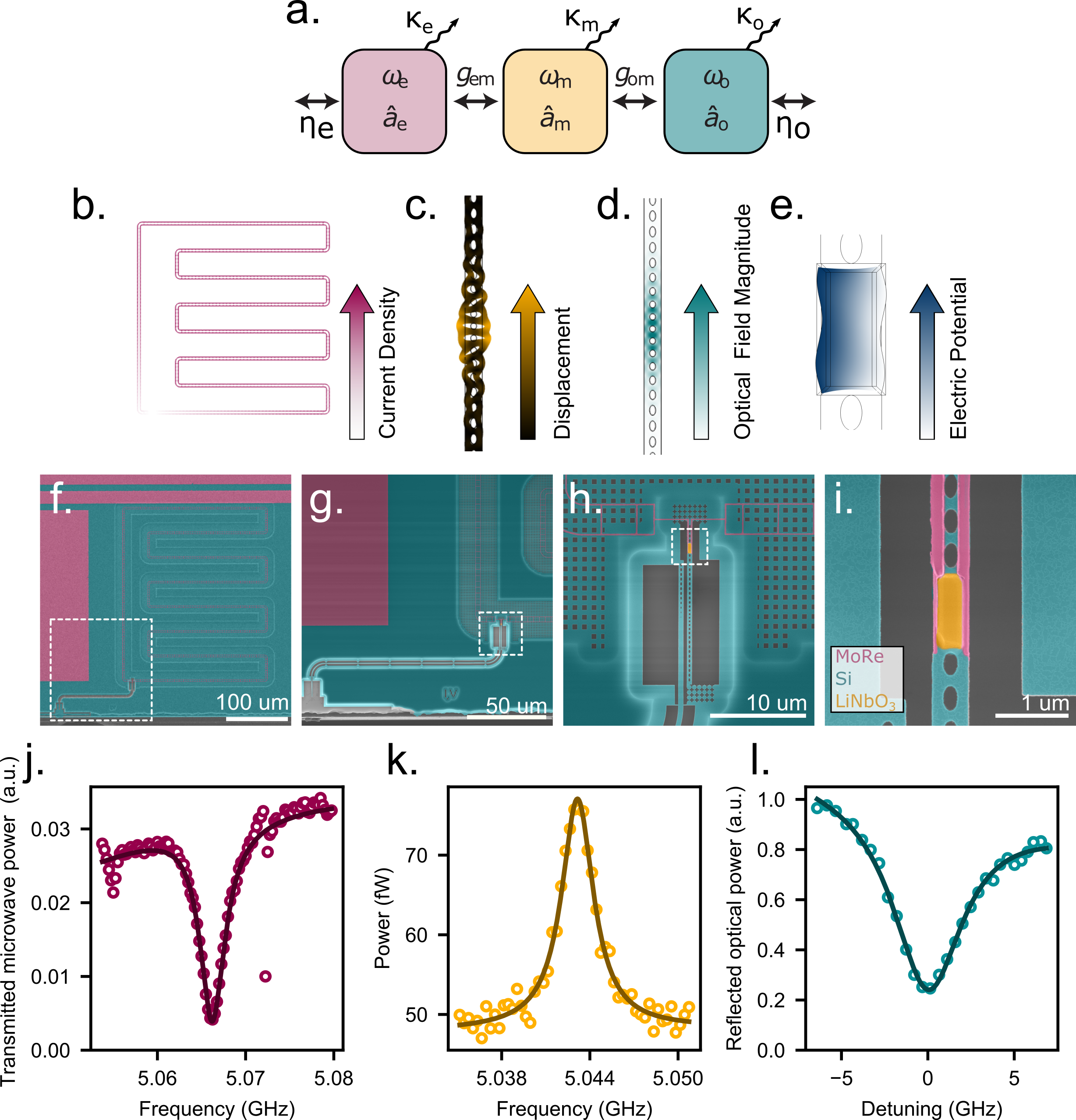
In order to efficiently couple microwave photons between the 50- transmission line and the high impedance piezoelectric device, we include a half-wavelength microwave resonator, terminated by the lithium niobate block (Fig. 1b,f). The resonator is formed from a 160-nm wide superconducting molybdenum-rhenium (\ceMoRe) nanowire. We pattern the resonator into a ladder geometry, which allows for tuning of the resonator frequency by up to 10% by applying a magnetic flux resulting from a nearby superconducting coil [35]. This tuning range ensures that we can match the microwave resonator to the mechanical mode frequency of the device. Simulations of the resulting electrical, mechanical and optical modes of the full device predict simultaneous single-photon optomechanical coupling strengths of kHz and piezoelectric coupling rates of up to MHz.
Our devices are fabricated from a 330 nm-thick layer of X-cut \ceLiNbO3 bonded to a high-resistivity silicon-on-insulator wafer. We first pattern and remove the lithium niobate layer through ion-beam-milling, leaving the small block shown in Figure 1i. We then pattern and etch the silicon layer to form the nanobeam (Fig. 1h). Finally, we deposit the film of \ceMoRe for the resonator and suspend the device by selectively etching the oxide layer. We use etch holes around the microwave resonator to remove the oxide layer from underneath, increasing the microwave quality factor of the device.
The device is cooled down to around 25 mK inside a dilution refrigerator. A laser field is coupled through a lensed optical fiber into a tapered reflective waveguide, which is evanescently coupled to the optical resonator, allowing us to measure the optical mode in reflection through a circulator [36]. As a first step, we characterise the device parameters. Figure 1l shows the overcoupled optical resonance we measure when scanning the input laser frequency and recording the reflected optical power. We find the device’s resonance at nm, with an external coupling rate GHz and intrinsic loss rate GHz. We characterise the mechanical spectrum of the device by stabilising the laser frequency red-detuned by with respect to the optical resonance and measuring the reflected signal through heterodyne detection. The resulting thermal spectrum of the mechanics is displayed in Figure 1k, showing a mode centred at GHz with a linewidth of MHz. The microwave resonator on the chip is capacitively coupled to a 50- transmission line. The microwave mode is measured in transmission and is displayed in Figure 1j, with a resonance centered at 5.07 GHz, an intrinsic loss-rate of MHz and an external coupling rate of MHz. This measurement was taken with a magnetic field of approximately 3 mT (see S.I. for full table of parameters).
We now proceed to characterise the interaction between the mechanical and the microwave sub-components. The electromechanical coupling is measured by applying a continuous microwave drive tone and tuning the microwave resonator’s frequency by applying a magnetic field (see Figure 2a). As the resonator frequency approaches the optically-active mechanical mode at 5.043 GHz, we observe the characteristic avoided-crossing of the resonance frequency, as the mechanical and electrical modes become hybridised. From the size of this avoided crossing, we can directly extract the coupling rate between the mechanical mode and the microwave mode, which is MHz, larger than and . This strong electromechanical coupling is evidence of the high-cooperativity interface required for efficient and noise-free transduction. Given the mechanical and electrical damping rates, we extract a cooperativity of .
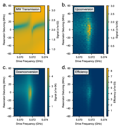
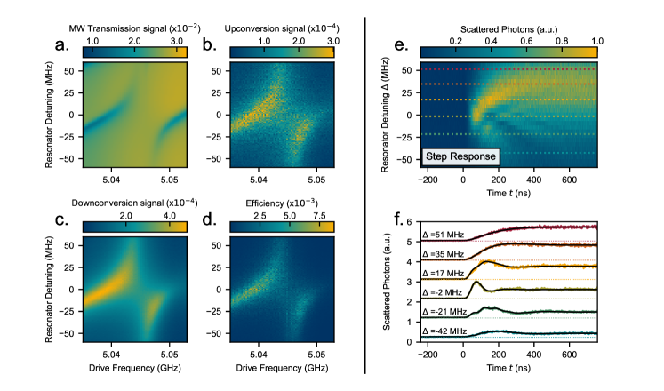
In order to demonstrate the microwave-to-optics transduction capabilities of the device (upconversion), we input a frequency-swept microwave tone which we convert with a continuous optical pump red-detuned from the optical resonance. We measure the up-converted signal by detecting the resulting optical sideband in the reflected light from the device through heterodyne-detection. In order to measure transduction from optics to microwave (downconversion), we supply a signal on-resonance with the optical cavity by modulating the red-detuned pump using an electro-optic modulator, and directly measuring the output microwave tone from the device. The upconversion and downconversion scattering parameters (including all microwave and optical loss and gain in the setup) as a function of the microwave drive and the detuning of the microwave resonator are displayed in Figure 2b and 2c, respectively. The transduction is at a maximum when the microwave-resonator approaches the mechanical frequency, and the two traces display the same avoided-crossing as in the microwave-spectroscopy.
We further supplement our continuous transduction measurements with measurements of the off-resonant reflected microwave and optical signals, which allow us to calibrate the loss and gain in the microwave and optical lines, and extract the bidirectional transduction efficiency of the transducer (see the Supplementary Information for details). We define transduction efficiency here as the waveguide to waveguide efficiency, excluding fiber coupling efficiency. The resulting 2-d map of efficiency is plotted in Figure 2d. We find that, for a supplied optical pump power of 1 the peak efficiency we extract is around 0.9 and with a bandwidth of MHz. For optical powers much greater than this, the efficiency is limited by non-linear effects such as thermal bistability of the optical cavity and reduction in the microwave-resonator quality factor due to residual absorption of the laser.
Pulsing the optical and microwave inputs allows us to access the time domain response of the device. We first look at the electromechanically enhanced excitation of the mechanical mode. In order to do this, we send in a continuous low-power optical drive and a fixed-frequency 2--long microwave pulse on resonance with the mechanical mode. We filter the upconverted signal from the reflected red-detuned pump light with narrow-linewidth Fabry-Pérot resonators [36]. The filtered light is detected using a superconducting nanowire single-photon detector (SNSPD). We correlate the arrival time of the photons following the start of the microwave pulse (at time =0). By sweeping the detuning of the microwave resonator with respect to the microwave tone, , and measuring the scattered photons from the device, as shown in Figure 2e,f, we can directly extract the time-dynamics of the transduction. As expected for a high-cooperativity interface, as the microwave resonator becomes resonant with the mechanical mode the rise time of the electro-mechanical loading is decreased and coherent oscillations between the resonator mode and the mechanical mode appear. We fit the time response to the microwave drive step with a simple model (see S.I.) to extract the electromechanical cooperativity of our device, which we find to be , in good agreement with the expected value for our independently measured parameters.
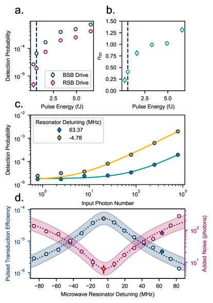
Now that we have characterized the time dynamics of the electromechanical interface, we move to also using short optical pulses. We start by measuring the thermal occupation of the mechanical mode as a function of pulse energy using a sideband asymmetry measurement [36]. We use 40 ns long optical pump pulses, filtering out the reflected optical pump and sending the scattered photons at the cavity frequency to the SNSPD (total detection efficiency, = 0.048). Figure 3a shows the resulting detection probabilities and a clear asymmetry between blue and red detuned pulses. The extracted thermal occupation () is shown in Figure 3b. For low pulse energies , indicating that the mechanical mode is with a high probability in the quantum ground state. As microwaves are first loaded into the mechanical resonator with an efficiency before thermal noise is added, the added noise referred to the input is photons. For the subsequent pulsed transduction measurements we operate in the regime where the added thermal noise to the transduction process is limited to photons.
For a full pulsed transduction characterization of our device we now input 60 ns long microwave pulses fixed at the mechanical frequency into the transducer, followed by a 40 ns red-detuned optical pulse at a repetition rate of 100 kHz. The converted optical output photons from the transducer are filtered and detected using the SNSPD. Figure 3c shows the photon detection probability as a function of input microwave photon number. The input microwave photon number is calibrated based on line attenuation measurements (see S.I.). The detected optical photons are the sum of the converted microwave photons () and the optomechanically converted noise photons (), where is the initial number of microwave photons, the overall detection efficiency, the optomechanical, and the electromechanical transduction efficiency, respectively. We then sweep the detuning of the microwave resonator with respect to the mechanical frequency and record the pulsed transduction efficiency and the added noise, , shown in Figure 3d. From this measurement we find a peak transduction efficiency of and minimum added noise of photons.
We can use our model from the transduction time dynamics (shown in Figure 2f) to determine the electromechanical loading efficiency. From the model we find an efficiency of , which is significantly higher than the extracted from the measurements in Figure 3d. From the microwave transmission data (see S.I.) we observe multiple strongly coupled modes which are relatively close in frequency to the mode of interest. By extending the model to include one extra neighboring mode, we see that the expected electromechanical loading efficiency drops to approximately 0.06 (see S.I.). With this reduced loading efficiency, the expected value for from the sideband asymmetry measurement is photons, in good agreement with the calibrated value above.
As a final step we investigate the limits of our transduction rate. To do this, we input a red-detuned laser into the cavity and determine the thermal occupation of the mechanical mode by measuring optomechanically scattered noise photons, without a microwave drive. We perform this measurement for increasing repetition rate, which is shown in Figure 4a. The relative thermal noise remains constant up to a repetition rate of approximately 100 kHz, above which, residual phonons from the previous excitation pulse increase the scattering rate. We find a thermal recovery time of 2 , which is around the same order of magnitude as the mechanical-mode lifetimes in the system.
We further measure the impact of optical light in the transducer on the frequency and quality factor of the superconducting resonator. Strong optical fields can pose a major challenge for integrated transducers as optical photons can generate quasiparticles (directly or via thermal heating) which degrade or even destroy the superconducting state [17]. In order to determine the impact of quasiparticle generation on our transducer, we measure the microwave resonance frequency shift and internal loss rate as a function of optical power (Fig. 4c,d). Individual traces without light and with the optical powers and wavelengths used in the continuous (1-W CW) and pulsed measurements (0.7-fJ pulses, 0.4-nW average power) are displayed in Figure 4b. We see a frequency shift of MHz and a times greater internal loss rate in the continuous case, but in the pulsed case only a frequency shift of kHz and a negligible loss rate change. We also repeat the optical power sweep 200-GHz detuned from the optical resonance and observe a drastically decreased response to optical power. We therefore conclude that the resonator changes are a result of the optical field inside the cavity, and that losses of the fiber-to-waveguide coupling play a negligible role. Overall, while we can observe some effects of quasiparticle generation, they are not significant enough to limit the low noise pulsed operation of our device.
Importantly, the bandwidth and repetition rates available with the transducer demonstrated here are already sufficient to interface with leading microwave-frequency quantum systems, such as superconducting qubits. The electromechanical efficiency for short microwave pulses can be further improved by optimizing the design of the piezoelectric interface to restrict coupling to near-resonant modes. Additionally, the noise contributions can be reduced with improved optical resonator linewidth, which is readily achievable through fabrication optimization; typical silicon-on-insulator optomechanical photonic crystal cavities have demonstrated intrinsic optical linewidths as low as 200 MHz [37]. When these improvements are combined, our transducer enters the regime where and creating entanglement between remote qubits will be feasible.
We have realized a new generation of microwave-to-optics transducers, based on an integrated mechanical mode that serves as an intermediary between the two electromagnetic fields. Constructing the device from thin-film lithium niobate on silicon allows us to realize efficient, low-noise, and large bandwidth transduction, through scalable fabrication techniques. We measure transduction efficiencies of 0.9% in the continuous and 5 in the pulsed regime, while adding only around 6 photons of input-referred noise.
The fully integrated device with a surface area of less than 0.15 mm2 only requires 1 nW of average laser power, allowing for repetition rates of up to 100 kHz. In terms of area and power dissipation, the current transducer design therefore directly allows for scaling to more than 10,000 transducers in a single dilution refrigerator. With optical frequency multiplexing, these transducers could be used to interface a large scale quantum processor using only around 100 fibers (with a predicted passive heatload of 300 pW [38]). Our device is also impedance matched to a 50- line, allowing flexible connections to qubits located within the same dilution refrigerator. This enables complete separation between the transduction and the qubit chip.
Our system is ideally suited to operate in the few-photon regime and optically read-out the state of a superconducting qubit, as has been recently demonstrated in another system [39]. Here the requirements on added noise and efficiency are relaxed and our current performance is sufficient to perform single-shot readout via the readout resonator of a qubit. Combined with optical multiplexing, this could lead to a system that replaces superconducting microwave amplifiers and cables, removing significant heatload and space restrictions inside a dilution refrigerator, enabling quantum processors to scale.
Acknowledgements.
We would like to thank Amir Safavi-Naeini for valuable discussions and support. We thank Jules van Owen and Damaz de Jong at Qblox for technical support. We further gratefully acknowledge assistance from Emma He, helpful discussions with Christophe Jurczak and Johannes Fink, supply of wafers from NGK Insulators Ltd. and the hospitality of the Department of Quantum Nanoscience at Delft University of Technology, as well as the Kavli Nanolab Delft. This work is financially supported by the European Innovation Council (EIC Accelerator QModem 190109269), the Province of Zuid-Holland (R&D samenwerkingsproject QConnect).Conflicts of interest
All authors declare a financial interest in QphoX B.V.
Data Availability
Source data for the figures will be made available on Zenodo.
References
- Kimble [2008] H. J. Kimble, The quantum internet, Nature 453, 1023 (2008).
- Wehner et al. [2018] S. Wehner, D. Elkouss, and R. Hanson, Quantum internet: A vision for the road ahead, Science 362, eaam9288 (2018).
- Alexeev et al. [2021] Y. Alexeev, D. Bacon, K. R. Brown, R. Calderbank, L. D. Carr, F. T. Chong, B. Demarco, D. Englund, E. Farhi, B. Fefferman, A. V. Gorshkov, A. Houck, J. Kim, S. Kimmel, M. Lange, S. Lloyd, M. D. Lukin, D. Maslov, P. Maunz, C. Monroe, J. Preskill, M. Roetteler, M. J. Savage, and J. Thompson, Quantum computer systems for scientific discovery, PRX Quantum 2, 017001 (2021).
- Ladd et al. [2010] T. D. Ladd, F. Jelezko, R. Laflamme, Y. Nakamura, C. Monroe, and J. L. O’Brien, Quantum computers, Nature 464, 45 (2010).
- de Leon et al. [2021] N. P. de Leon, K. M. Itoh, D. Kim, K. K. Mehta, T. E. Northup, H. Paik, B. S. Palmer, N. Samarth, S. Sangtawesin, and D. W. Steuerman, Materials challenges and opportunities for quantum computing hardware, Science 372, eabb2823 (2021).
- Chow et al. [2021] J. Chow, O. Dial, and J. Gambetta, IBM Research Blog (2021).
- Awschalom et al. [2021] D. Awschalom, K. K. Berggren, H. Bernien, S. Bhave, L. D. Carr, P. Davids, S. E. Economou, D. Englund, A. Faraon, M. Fejer, S. Guha, M. V. Gustafsson, E. Hu, L. Jiang, J. Kim, B. Korzh, P. Kumar, P. G. Kwiat, M. Lončar, M. D. Lukin, D. A. Miller, C. Monroe, S. W. Nam, P. Narang, J. S. Orcutt, M. G. Raymer, A. H. Safavi-Naeini, M. Spiropulu, K. Srinivasan, S. Sun, J. Vučković, E. Waks, R. Walsworth, A. M. Weiner, and Z. Zhang, Development of quantum interconnects (QuICs) for next-generation information technologies, PRX Quantum 2, 017002 (2021).
- Krastanov et al. [2021] S. Krastanov, H. Raniwala, J. Holzgrafe, K. Jacobs, M. Lončar, M. J. Reagor, and D. R. Englund, Optically-Heralded Entanglement of Superconducting Systems in Quantum Networks, Phys. Rev. Lett. 127, 040503 (2021).
- Bravyi et al. [2022] S. Bravyi, O. Dial, J. M. Gambetta, D. Gil, and Z. Nazario, The Future of Quantum Computing with Superconducting Qubits, arXiv:2209.06841 (2022).
- Magnard et al. [2020] P. Magnard, S. Storz, P. Kurpiers, J. Schär, F. Marxer, J. Lütolf, J.-C. Besse, M. Gabureac, K. Reuer, A. Akin, B. Royer, A. Blais, and A. Wallraff, Microwave quantum link between superconducting circuits housed in spatially separated cryogenic systems, Phys. Rev. Lett. 125, 260502 (2020).
- McKenna et al. [2020] T. P. McKenna, J. D. Witmer, R. N. Patel, W. Jiang, R. V. Laer, P. Arrangoiz-Arriola, E. A. Wollack, J. F. Herrmann, and A. H. Safavi-Naeini, Cryogenic microwave-to-optical conversion using a triply resonant lithium-niobate-on-sapphire transducer, Optica 7, 1737 (2020).
- Xu et al. [2021] Y. Xu, A. A. Sayem, L. Fan, C. L. Zou, S. Wang, R. Cheng, W. Fu, L. Yang, M. Xu, and H. X. Tang, Bidirectional interconversion of microwave and light with thin-film lithium niobate, Nature Commun. 12, 4453 (2021).
- Sahu et al. [2022] R. Sahu, W. Hease, A. Rueda, G. Arnold, L. Qiu, and J. M. Fink, Quantum-enabled operation of a microwave-optical interface, Nature Commun. 13, 1276 (2022).
- Vainsencher et al. [2016] A. Vainsencher, K. J. Satzinger, G. A. Peairs, and A. N. Cleland, Bi-directional conversion between microwave and optical frequencies in a piezoelectric optomechanical device, Appl. Phys. Lett. 109, 033107 (2016).
- Higginbotham et al. [2018] A. P. Higginbotham, P. S. Burns, M. D. Urmey, R. W. Peterson, N. S. Kampel, B. M. Brubaker, G. Smith, K. W. Lehnert, and C. A. Regal, Electro-optic correlations improve an efficient mechanical converter, Nature Phys. 14, 1038 (2018).
- Jiang et al. [2020] W. Jiang, C. J. Sarabalis, Y. D. Dahmani, R. N. Patel, F. M. Mayor, T. P. McKenna, R. Van Laer, and A. H. Safavi-Naeini, Efficient bidirectional piezo-optomechanical transduction between microwave and optical frequency, Nature Commun. 11, 1166 (2020).
- Mirhosseini et al. [2020] M. Mirhosseini, A. Sipahigil, M. Kalaee, and O. Painter, Superconducting qubit to optical photon transduction, Nature 588, 599 (2020).
- Stockill et al. [2021] R. Stockill, M. Forsch, F. Hijazi, G. Beaudoin, K. Pantzas, I. Sagnes, R. Braive, and S. Gröblacher, Ultra-low-noise Microwave to Optics Conversion in Gallium Phosphide, arXiv:2107.04433 (2021).
- Han et al. [2018] J. Han, T. Vogt, C. Gross, D. Jaksch, M. Kiffner, and W. Li, Coherent microwave-to-optical conversion via six-wave mixing in rydberg atoms, Phys. Rev. Lett. 120, 093201 (2018).
- Fernandez-Gonzalvo et al. [2019] X. Fernandez-Gonzalvo, S. P. Horvath, Y. H. Chen, and J. J. Longdell, Cavity-enhanced raman heterodyne spectroscopy in Er3+: Y2SiO5 for microwave to optical signal conversion, Phys. Rev. A 100, 033807 (2019).
- Bartholomew et al. [2020] J. G. Bartholomew, J. Rochman, T. Xie, J. M. Kindem, A. Ruskuc, I. Craiciu, M. Lei, and A. Faraon, On-chip coherent microwave-to-optical transduction mediated by ytterbium in YVO4, Nature Commun. 11, 3266 (2020).
- Hisatomi et al. [2016] R. Hisatomi, A. Osada, Y. Tabuchi, T. Ishikawa, A. Noguchi, R. Yamazaki, K. Usami, and Y. Nakamura, Bidirectional conversion between microwave and light via ferromagnetic magnons, Phys. Rev. B 93, 174427 (2016).
- Lauk et al. [2020] N. Lauk, N. Sinclair, S. Barzanjeh, J. P. Covey, M. Saffman, M. Spiropulu, and C. Simon, Perspectives on quantum transduction, Quantum Sci. Technol. 5, 20501 (2020).
- Han et al. [2021] X. Han, W. Fu, C.-L. Zou, L. Jiang, and H. X. Tang, Microwave-optical quantum frequency conversion, Optica 8, 1050 (2021).
- Siddiqi [2021] I. Siddiqi, Engineering high-coherence superconducting qubits, Nature Rev. Mat. 10, 875 (2021).
- Krinner et al. [2022] S. Krinner, N. Lacroix, A. Remm, A. Di Paolo, E. Genois, C. Leroux, C. Hellings, S. Lazar, F. Swiadek, J. Herrmann, G. J. Norris, C. K. Andersen, M. Müller, A. Blais, C. Eichler, and A. Wallraff, Realizing repeated quantum error correction in a distance-three surface code, Nature 605, 669 (2022).
- Horsman et al. [2012] C. Horsman, A. Fowler, S. Devitt, and R. van Meter, Surface code quantum computing by lattice surgery, New J. Phys. 14, 123011 (2012).
- Beals et al. [2013] R. Beals, S. Brierley, O. Gray, A. W. Harrow, S. Kutina, N. Linden, D. Shepherd, and M. Stather, Efficient distributed quantum computing, Proc. R. Soc. A 469, 20120686 (2013).
- Krinner et al. [2019] S. Krinner, S. Storz, P. Kurpiers, P. Magnard, J. Heinsoo, R. Keller, J. Lütolf, C. Eichler, and A. Wallraff, Engineering cryogenic setups for 100-qubit scale superconducting circuit systems, EPJ Quantum Technol. 6, 2 (2019).
- Zeuthen et al. [2020] E. Zeuthen, A. Schliesser, A. S. Sørensen, and J. M. Taylor, Figures of merit for quantum transducers, Quantum Sci. Technol. 5, 34009 (2020).
- Brubaker et al. [2022] B. M. Brubaker, J. M. Kindem, M. D. Urmey, S. Mittal, R. D. Delaney, P. S. Burns, M. R. Vissers, K. W. Lehnert, and C. A. Regal, Optomechanical ground-state cooling in a continuous and efficient electro-optic transducer, Phys. Rev. X 12, 021062 (2022).
- Jiang et al. [2022] W. Jiang, F. M. Mayor, S. Malik, R. V. Laer, T. P. McKenna, R. N. Patel, J. D. Witmer, and A. H. Safavi-Naeini, Optically heralded microwave photons, arXiv:2210.10739 (2022).
- Chan et al. [2012] J. Chan, A. H. Safavi-Naeini, J. T. Hill, S. Meenehan, and O. Painter, Optimized optomechanical crystal cavity with acoustic radiation shield, App. Phys. Lett. 101, 081115 (2012).
- Aspelmeyer et al. [2014] M. Aspelmeyer, T. J. Kippenberg, and F. Marquardt, Cavity optomechanics, Rev. Mod. Phys. 86, 1391 (2014).
- Xu et al. [2019] M. Xu, X. Han, W. Fu, C.-L. Zou, and H. X. Tang, Frequency-tunable high- Q superconducting resonators via wireless control of nonlinear kinetic inductance, Appl. Phys. Lett. 114, 192601 (2019).
- Riedinger et al. [2016] R. Riedinger, S. Hong, R. A. Norte, J. A. Slater, J. Shang, A. G. Krause, V. Anant, M. Aspelmeyer, and S. Gröblacher, Non-classical correlations between single photons and phonons from a mechanical oscillator, Nature 530, 313 (2016).
- Zivari et al. [2022] A. Zivari, R. Stockill, N. Fiaschi, and S. Gröblacher, Non-classical mechanical states guided in a phononic waveguide, Nature Phys. 18, 789 (2022).
- Lecocq et al. [2021] F. Lecocq, F. Quinlan, K. Cicak, J. Aumentado, S. A. Diddams, and J. D. Teufel, Control and readout of a superconducting qubit using a photonic link, Nature 591, 575 (2021).
- Delaney et al. [2022] R. D. Delaney, M. D. Urmey, S. Mittal, B. M. Brubaker, J. M. Kindem, P. S. Burns, C. A. Regal, and K. W. Lehnert, Superconducting-qubit readout via low-backaction electro-optic transduction, Nature 606, 489 (2022).
- Andrews et al. [2014] R. W. Andrews, R. W. Peterson, T. P. Purdy, K. Cicak, R. W. Simmonds, C. A. Regal, and K. W. Lehnert, Bidirectional and efficient conversion between microwave and optical light, Nature Phys. 10, 321 (2014).
- Hong et al. [2017] S. Hong, R. Riedinger, I. Marinković, A. Wallucks, S. G. Hofer, R. A. Norte, M. Aspelmeyer, and S. Gröblacher, Hanbury Brown and Twiss interferometry of single phonons from an optomechanical resonator, Science 358, 203 (2017).
Supplementary Information
I Fabrication Details
The starting material for these devices is a thin film of X-cut LiNbO3 (LN) bonded on a high resistivity silicon-on-insulator (SOI) substrate. The full device fabrication consists of four main steps. First, an Ar milling process patterns the LN layer to form small blocks. Second, a reactive-ion etch (RIE) step forms the nanobeams. Third, deposition of a MoRe layer and lift-off creates the bondpads, the feedline, and the resonators. Finally, an oxide etch selectively removes the sacrificial SiO2 layer underneath the Si device layer to suspend the devices. This step also removes the oxide under the resonators, increasing the electrical quality factor of the devices.
II Experimental Details
| Parameter name | Parameter Description | Value | Error | Units |
| Device Property | ||||
| Mechanical Frequency | 5.043 | GHz | ||
| Optical Frequency | 193.087 | THz | ||
| Mechanical Linewidth | 2.63 | 0.12 | MHz | |
| Electrical Linewidth | 3.439 | 0.144 | MHz | |
| External Electrical Coupling Rate | 2.213 | 0.097 | MHz | |
| Intrinsic Electrical Loss Rate | 1.226 | 0.106 | MHz | |
| Optical Linewidth | 4.99 | 0.19 | GHz | |
| External Optical Coupling Rate | 3.65 | 0.14 | GHz | |
| Intrinsic Optical Loss Rate | 1.34 | 0.07 | GHz | |
| Electrical Resonator Coupling | 0.322 | 0.019 | ||
| Optical Resonator Coupling | 0.731 | 0.040 | ||
| Single Photon Optomechanical Coupling Rate | 561 | 51 | kHz | |
| Electromechanical Coupling Rate | 7.4 | 0.9 | MHz | |
| Experimental Setup | ||||
| Fiber Coupling Efficiency | 0.42 | 0.03 | ||
| Filter Transmission Efficiency | 0.19 | 0.03 | ||
| SNSPD Detection Efficiency | 0.60 | 0.03 | ||
| Line attenuation fridge and external | -113.6 | 0.2 | dB |
Our experimental setup consists of a microwave and an optical interface for the transducer as shown in Figure S1. The transducer is located on the baseplate of a dilution refrigerator at a temperature of around 25 mK. Microwave lines with attenuators deliver the microwave input signals to the baseplate and then to the transmission line on the sample. The output of the on-chip transmission line is connected to two circulators and then to a high-electron-mobility transistor (HEMT) amplifier at 4K and a room temperature amplifier. Microwave signals are generated with a microwave source with a fast microwave switch or a vector network analyser (VNA) and detected with a VNA.
The optical input path consists of a pulsed path and a continuous path. For continuous mode transduction we lock the laser red-detuned from the optical cavity by and pass it through an amplitude electro-optic modulator (EOM). The optical input signal for downconversion is generated by driving the EOM at and generating a sideband at the cavity frequency. For pulsed transduction, we generate pulses with a function generator driving an acousto-optic modulator (AOM). The optical input is passed through a fiber into the cryostat and on the baseplate we couple the light into the on chip waveguide of the transducer with a lensed fiber tip.
We seperate the reflected output optical signal from the input signal with a circulator. For continuous mode transduction we detect the output signal with heterodyne detection using a high bandwidth photodiode. For pulsed transduction we pass the output signal through two filter cavities to remove the optical pump. We then pass the signal back into the refrigerator for detection and photon counting on a single photon detector (SNSPD) [36]. The total detection efficiency is = 4.8%.
For continuous mode transduction we determine the transduction efficiency with a four port VNA measurement using the method developed by Andrews et al. [40]. By measuring the microwave attenuation in the microwave input and output () and the microwave attenuation in the optical input and output (), we can calibrate the input and output losses, which are included in the upconversion () and downconversion () measurements. The EOM generates two sidebands; both contribute to , but only the sideband resonant with the cavity contributes to . Therefore the continuous transduction efficiency, , is given by:
| (S1) |
where the pre-factor corresponds to the reduction in we measure for a carrier red-detuned by 5-GHz compared to a fully off-resonant tone. Because the method cancels all common paths, the bidirectional continuous transduction efficiency we measure here is from one port of the on-chip microwave waveguide to the on-chip optical waveguide.
In the strong coupling electro-mechanical regime, the measurement of the transduction bandwidth is complicated as the efficiency no longer follows a Lorentzian lineshape from which we can extract a full width at half maximum (FWHM). However, high transduction efficiency is maintained across the whole avoided crossing with a separation given by 2. Therefore we use 2 MHz as the transduction bandwidth in the main text. Increasing further by reducing the gap between the resonator and the feedline woudl
Measured device and setup parameters are included in Table 1. All parameters are measured for the device described in the main text, apart from the value of . We extract this parameter from the scattering probability in the pulsed experiment shown in Figure 3 a-b, following the same method as in [41].
III Microwave Input Loss Calibration
For continuous wave transduction we can use a four port measurement to remove external setup losses from the transduction efficiency. However, in the case of pulsed microwave to optics transduction, we need to calibrate the input microwave losses to the transducer to determine the efficiency and added noise. Because microwave losses are temperature dependent, directly measuring losses through the cables at room temperature gives only an estimate of the input microwave loss. In this section we describe an alternative measurement of the input microwave loss.
We use a three line measurement to directly measure the losses. The three lines are the input microwave line which drives the transducer and two additional microwave lines with no added attenuation, which are nominally identicle. We connect the three lines via a 3-port circulator. We measure the transmission from one unattenuated line to the other, subtract circulator losses and divide by 2 to determine an unattenuated line loss of dB. We then measure the losses going through the drive line and one attenuated line and subtract circulator losses and the unattenuated line loss, arriving at a microwave drive line attenuation of dB.
The connection between the microwave drive line and the device is more uncertain. The connecting wire between the drive line and the device has an attenuation of dB at room temperature. However, typically attenuation decreases at low temperatures and we must add any chip connector losses. Given these systematic uncertainties we estimate a loss for this segment of dB. and transduction efficiency in Figure 3c of the main text show a shaded region corresponding to a line attenuation of dB.
To measure the pulsed transduction efficiency we calibrate the input microwave photons with the sum of the measured dilution refrigerator and external line attenuation (). The pulsed transduction efficiency, is defined as:
| (S2) |
is the mean number of photons detected on the detector per excitation pulse. , and are the microwave power, duration and frequency of the excitation pulse at the output of the microwave generator. The pulsed transduction efficiency is the on-chip microwave waveguide to on-chip optical waveguide transduction efficiency, as in the continuous case.
IV Microwave Resonator Tuning and Coupling
Our microwave resonators are laddered kinetic inductance resonators similar to those implemented by Xu et al. [35]. By including loops in the wire, the kinetic inductance can be increased with the application of a magnetic field, tuning the frequency. We mount a coil close to the sample to generate the magnetic field. Figure S2 displays magnetic field tuning for three microwave resonators coupled to a single transmission line. We fit the resonance frequency of the resonator used in the main text as a function of coil current (Figure S2a-e) and extract a tuning rate of 1.8 GHz (Figure S2f). We estimate the magnetic field at the resonator to be mTA. In total, we can achieve up to 500 MHz of tuning.
In Figure S2g, we also scan the microwave transmission in a narrower range around the transduction frequency. There are a number of avoided crossings close to the transduction frequency, corresponding to other mechanical modes of the system.
V Electromechanical Theoretical Model
We use a simplification of the model outlined by Han et al. [24] to determine the time dynamics of energy transfer between modes. This model can be used to describe all mechanical, electrical and optical modes in the system. In our specific case, we operate in the regime where . In this regime the optical emission from the transducer is directly proportional to the mechanical occupation of the transduction mode and both the optical driving field and the occupation of the optical cavity mode have negligible effect on the occupation of the mechanical resonator.
The model involves a first order differential equation for the time evolution [24]:
| (S3) |
and are the microwave and mechanical mode occupancies. and are the detuning of the microwave resonator and the mechanical mode from the drive frequency respectively and is a parameter proportional to the microwave power sent into the transmission line. We can analytically solve this equation and find the time dynamics of the mode populations as a function of , , and time. We numerically fit the function of , and to the time dynamics in Figure 2e,f of the main text and extract the parameters and . The model succesfully explains the key features of electromechanical loading with long, 2 s pulses.
We also investigate the loading efficiency with the short 60 ns microwave pulses we used in Figure 3 of the main text. We plot the mode occupation of the microwave resonator and mechanical mode when the systen is driven with a single microwave photon in Figure S3. Energy is exchanged between the two modes as expected for the strong coupling of our device. We reach a peak phonon population or loading efficiency of 0.12, which is greater than the measured value for loading efficiency. This motivates us to investigate some of the other mechanical modes in the system (see Figure S2g).
We extend the model to include an extra parasitic mechanical mode:
| (S4) |
and are the second mode population, the electromechanical coupling rate for the second mode, the detuning of the drive from the second mode and the mechanical loss rate of the second mode. We plot the time response for the above derived parameters, = 17 MHz, = 28 MHz and , the approximate parameters of the large avoided crossing closest below the frequency of the main mode in Figure S3. We did not measure , but the exact value does not have a large impact on the results.
We see a large decrease in the mode occupation of both the microwave and mechanical modes in the extended double mode model compared to the single mode model. In particular the maximum phonon occupation drops to 0.06. This leads to a decrease in the electromechanical loading efficiency. If we put in the parameters for other neighboring mechanical modes, the maximum phonon occupation also drops, but only by 5%. Determining the exact mode couplings and loss rates is left to a future investigation.
For long pulses (for example 2 s as used in Figure 2 e,f of the main text) and continuous driving, we see negligible differences between the single mode and double mode model results. The insensitivity to other mechanical modes is caused by the reduced bandwidth of longer pulses compared to the 60 ns pulses. With a reduced bandwidth for the drive, the detuning is much larger than the bandwidth resulting in only a small interaction.
VI Sideband Asymmetry Power Correction
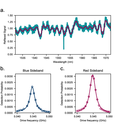
Our devices are fabricated with a 150 m long extended optical waveguide to prevent stray light from the coupling lensed fiber directly impacting the microwave resonator. Reflections at the beginning (and to a lesser extent at the supporting tethers) of the waveguide generate Fabry-Perot type interferences in the reflection from the waveguide. This is visible in the oscillations of the reflected signal of the long wavelength scan of Figure S4a. We see that the much deeper and narrower reflection dip from the optical cavity is superimposed on this oscillation.
Although the reflections that cause these oscillations are small, they also affect the optical power delivered to the microwave cavity as a function of detuning. We measure the relative optical cavity occupation with the pump laser detuned red and blue by the mechanical frequency by exciting the mechanical transduction mode to a large occupation with a microwave drive via the transmission line and detuned microwave resonator. For the large estimated mechanical occupations of order 100 phonons, the optomechanical scattering rate differences between red and blue sideband should be negligible. We measure, however in Figure S4b and c, that the detection probability of photons from the two sidebands is quite different, which we directly attribute to the wavelength dependent interferences in the waveguide.
In the main text we measure the asymmetry in detection rates as a means to extract the thermal occupation of the mechanical mode. This technique assumes equal optical cavity occupation for both sidebands. Therefore in order to satisfy this assumption, we adjust the optical input power we send to the device by increasing the blue detuned power by a factor of 1.53, the ratio of the fitted peaks in Figure S4. Repeating this calibration with the other optomechanical mode at 5.072 GHz or with continuous optical driving and heterodyne detection gives a similar correction factor, indicating that it is not mechanical mode or collection path dependent.
VII Other transduction mode
In addition to the many electromechanically active modes, there are also multiple optomechanicallly active modes. We can use another of these modes to operate the transducer at a different frequency, GHz. We measure the CW conversion of the transducer with a 4-port measurement using the same techniques for the other transduction mode. We find that this mode is less strongly coupled with a smaller MHz. The mechanical linewidth of this mode is also smaller with MHz. The conversion again displays an avoided crossing between the microwave and mechanical modes with a peak efficiency of 0.5% with 1 W input power (see Figure S5).