Controlled generation and detection of a thermal bias in Corbino devices under the quantum Hall regime.
Abstract
We present an experimental technique to generate and measure a temperature bias in the quantum Hall effect of GaAs/AlGaAs Corbino samples. The bias is generated by injecting an electrical current at a central resistive heater and the resulting radial temperature drop is determined by conductance measurements at internal and external concentric rings. The experimental results agree with the predictions of numerical simulations of the heat flow through the substrate. We also compare these results with previous predictions based on the thermoelectric response of these devices.
The quantum Hall effect (QHE) [1] has been a cornerstone to many fundamental phenomena in physics since its discovery more than 40 years ago [1]. It also has a key role in electrical metrology and in the 2019 redefinition of the International System of Units [2]. Two very interesting sides of this effect, which motivated several insightful experiments, are its thermal [3, 4, 5, 6, 7, 8, 9, 10] and thermoelectric [11, 12, 13, 14, 15, 16, 17, 18] properties. The related research activity, along with the study of these properties in other mesoscopic devices is accompanied by the development of reliable techniques for temperature sensing [19].
A large body of work on thermal and thermoelectric transport in the quantum Hall regime focuses on the edge states, where the transport takes place through a few ballistic channels. This is an ideal playground to study many fundamental properties from the theoretical [20, 21, 22, 23] and experimental point of view. Prominent experimental examples are the investigation of the chiral propagation of heat [8, 3, 24], the study of the peculiar transport of charge and energy in some fractional filling factors [4, 25], and the detection of the quantum of thermal conductance [10]. The main experimental strategy to induce thermal transport in this context is the implementation of ohmic contacts at the edge states. Local temperature sensing relies on recording the conductance in tunnel-coupled quantum dots in the Coulomb blockade regime, playing the role of thermometers [3, 4, 5, 6, 7], or noise analysis [9, 10].
A different scenario, albeit equally interesting, is expected to take place in the thermal and thermoelectric transport through the Landau levels, the bulk states of the quantum Hall regime. Relatively less experimental results have been reported on these phenomena in comparison to those on the edge states. Efforts in this direction by Chickering et al. [11], Liu et al. [16] and Endo et al. [15] focus on implementations using the Hall bar setup. In this geometry, the thermal and thermoelectric response functions have a tensorial structure with coupled longitudinal and transverse components akin to the electrical ones. As highlighted in the theoretical work of Ref. [26], the electrical and thermal properties of the Landau levels can be more directly assessed in the Corbino (ring) geometry. The reason is that an electrical and/or thermal bias radially applied in the Corbino configuration generate radial fluxes in the bulk states, which are decoupled from the transverse ones. This motivated recent studies of thermoelectric transport [17, 18, 27, 28], complementing earlier experimental [14] and theoretical results [29].
The goal of this contribution is the proposal of an experimental method to study the thermal and thermoelectric transport through the Landau levels of a two-dimensional electron system (2DES) under the quantum Hall regime of a Corbino device. This consists in the controlled generation of a temperature bias in the 2DES as well as its corresponding sensing. Importantly, because Landau levels extend throughout the bulk of the sample, edge-state techniques such as those in Refs. [8, 3, 4, 5, 6, 7], cannot be used.
We focus on the experimental setup shown in Fig. 1 (a), where the central region of the sample is heated using an electrical resistor and the outer rim is connected to the cold finger of a cryostat. To generate the thermal bias, it is important to notice that the 2DES has a thermal conductivity which is much lower than that of the phonons in the substrate [11, 12]. Hence, the latter defines the limit to establish the temperature gradient in the substrate, while the 2DES locally thermalizes with it. To sense the temperature drop at the 2DES, a series of five concentric electrical contacts are implemented within the Corbino disk [yellow areas in Fig. 1 (a)]. These contacts define four regions of the 2DES, labeled as rings 1,2,3 and 4. We measure the conductance of rings 1 and 4 and use its dependence on temperature to sense the temperature drop between the ring 1 and 4. We compare these measurements with numerical estimates of the temperature gradient in the substrate, based on calculations of the phononic heat flux through the substrate and find excellent agreement. Furthermore, we demonstrate that there exists a linear relationship between the power applied to the heater and the temperature gradient in the sample.
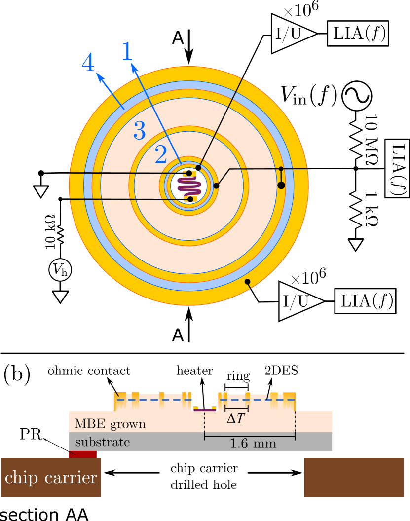
The single 2DES forms in a GaAs/AlGaAs heterostructure, grown by molecular beam epitaxy on a GaAs wafer. Control samples measured independently at in the dark, resulted in 2DES mobilities and densities of the order of and , respectively. Using micro-processing techniques, a ring-shaped mesa and ohmic contacts of Ni-Ge-Au are implemented on square-cleaved samples. The final configuration has four concentric rings defined by the five ohmic contacts. The internal and external diameters of the full Corbino structure hosting the four rings are, respectively, and . The central AuPd heater is placed outside the mesa. The sample is placed on a chip carrier, which is in contact with a 3He cold finger cryostat of base temperature. The chip carrier is drilled to contain a central hole with a diameter of in order to minimize the thermal contact with the substrate. Only one side of the sample is glued to it [see PR in the left hand side of Fig.1 (b)]. The temperature at the cold finger is recorded with a Cernox sensor. The magnetic field is generated by a superconducting magnet.
Magneto-transport measurements can be performed independently in any of the 4 rings by suitably connecting the two consecutive ohmic contacts that define the ring to be measured. We have confirmed that the four rings exhibit independent responses. For the measurements of the conductance () a ac voltage is applied to the system via a voltage divider. The induced electrical current is then measured by a lock-in amplifier (LIA) and a current-to-voltage amplifier (IUamp), whose frequency response has been previously verified to be flat within the measurement range. We focus on measurements at a fixed magnetic field , corresponding to Landau level , because the conductance at this magnetic field shows a clear dependence on the temperature, allowing a good resolution for the temperature calibration. We will further discuss this choice below.
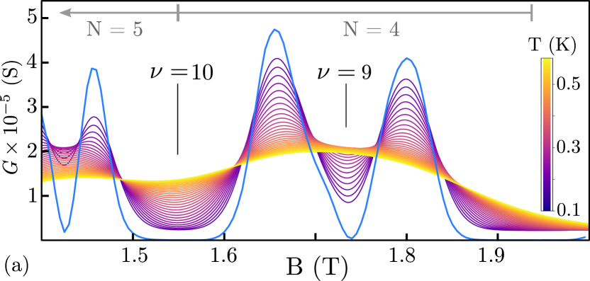
The crucial property to sense the temperature is the dependence of the magneto-conductance of the different rings as a function of the temperature. Given the transmission function , characterizing the transparency of the device and determined by its microscopic details, the conductance reads
| (1) |
where is the Fermi-Dirac distribution function, which depends on the temperature and the chemical potential . Our procedure is based on performing independent measurements of the conductance of the rings 1 and 4. Ideally, by using the temperature dependence predicted by Eq. (1) we could define the average temperature of the 2DES in the area enclosed by each of these rings. However, it is not possible to have an exact and accurate expression for the function for each ring and for all values of . Therefore, we introduce a fully experimental protocol to define the average temperature of a given ring on the basis of the measurements of its conductance. One important aspect is to identify a regime where there is a one-to-one correspondence between and . To this end, before implementing the experimental protocol, we carry out some preliminary theoretical estimates by inferring the transmission function following Ref. 18 (this approach leads to accurate results at high magnetic fields as ). We show in Fig. 2 (a) results of the evolution of the conductance of ring 1 for different temperatures calculated using a transmission function inferred from the data of . While we are not able to accurately fit the data for any , these plots are useful for seeing semi-quantitative features of the evolution of the conductance with . In particular, we notice that is a monotonous increasing function of temperature, which is a useful property to define a one-to-one correspondence between and . For this reason, we focus on this value of the magnetic field in our analysis.
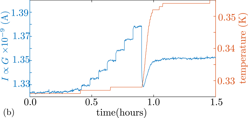
We now turn to discuss the experimental protocol. The first step is to record the conductance without any power applied to the central heater. We consider bath temperatures between and , as measured with the cold finger thermometer. In this way, we obtain a one-to-one relation between temperature of the 2DES and conductance. Therefore, becomes our calibration curve. The second step is to record the conductance at Corbino rings 1 and 4 for different values of the heater power and bath temperatures. After each bath temperature change, we wait at least ten minutes for thermalization, until the temperature fluctuation is lower than . When the conductance reaches a stable value we perform a set of measurements changing the DC heater power. This process is repeated for different bath temperatures. As an example, Fig. 2 shows a set of simultaneous measurements of the conductance and temperature over time.
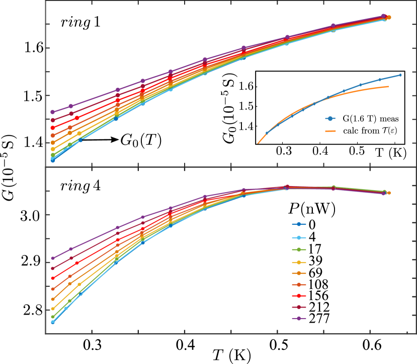
The sets of conductance measurements in the two rings at , for different base temperatures and for several heater powers are plotted in Fig. 3. For the case of ring 1, we also show in the inset of panel (a), the measurements at zero power along with the prediction based on Eq. (1), and we observe a good semi-quantitative agreement. The deviation should be traced back to the fact that the function has not been inferred from data at low enough temperature. The results for ring 4 are shown in panel (b). The behavior of the conductance of the two rings as a function of the temperature is not exactly the same. In particular, a non-monotonous behavior observed in the ring 4 in contrast with that of ring 1. This is a consequence of inhomogeneities and charge density fluctuations along the sample. Nevertheless, we see that below the conductance is a monotonous function of the temperature for all power levels in both rings. This defines a useful range of temperatures to identify a one-to-one correspondence between the conductance value and the temperature. Here, we use the calibration of obtained at zero heater power to define the mean local temperatures of rings at different powers since we can associate each measured conductance to a 2DES temperature. The procedure simply corresponds to drawing a horizontal line in the corresponding panel of Fig. 3, starting at the measured conductance of the ring until intersecting . The horizontal coordinate of the intersection point defines .
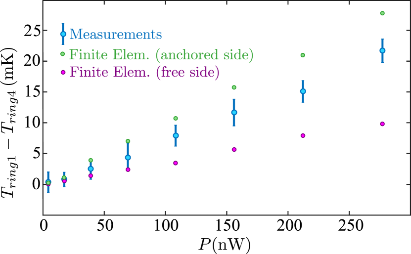
The temperature difference is determined from the estimates of the temperatures of the two rings. This temperature difference is obtained at fixed values of the heater power by averaging the results over a cold finger temperature range from . Results are shown in Fig. 5, where we verify a linear dependence between these two quantities. The error bars indicate the statistical errors associated with the averaging procedure.
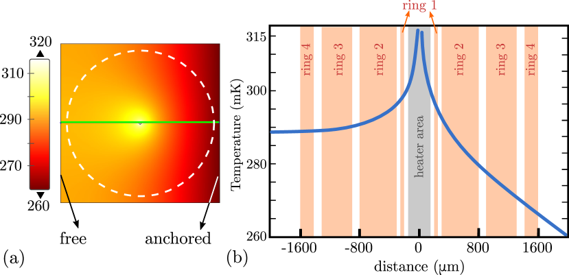
To benchmark the previous estimates for the temperature difference induced in the 2DES we simulate the temperature profile using values of the thermal conductivity of the substrate previously reported in the literature at , [11, 12] (following a law ). In these works, it was shown that the substrate phonons determine the temperature gradient at mK temperatures as we are assuming here. This is supported by the fact that the estimate for the conductivity of the 2DES is , i.e., orders of magnitude smaller.
We performed finite-element simulations of the heat-flow equation, its results for a heater power of are shown in the color-map of Fig. 4. Following the experimental setup, only the side indicated as anchored is assumed to be thermalized at the temperature of the cold finger, while the other edges have free contour conditions.
The calculated temperature differences are shown in Fig. 5, together with the experimental results. Estimates for the anchored side at a power of , for instance, is , while in the free side, the temperature difference results to be . Averaging these results, as the experiment does when integrating over the ring ohmic contacts, we obtain , in good agreement with the measured value of .
To finalize, we also compare the estimates for this temperature difference to the ones inferred from thermoelectric measurements. In the latter case, the thermal gradient is generated by applying an ac voltage to the heater with a period of , which is much longer than the typical relaxation rate of the electrons. At this frequency range, the thermal distribution can be modeled by the stationary behavior. Deviations are expected only at much higher frequencies. The resulting current of amplitude and angular frequency results in a power given by , being a possible arbitrary phase and is the resistance of the heater. The generated temperature bias between the heater and the external rim of the structure can be assumed to have the following behavior
| (2) |
with , independent of the frequency.
According to the measurements of thermal voltage reported in Ref. 18 under similar experimental conditions as in the present work (same device, power of and a bath temperature of ), the estimate for the oscillating component of the temperature bias for the ring 2 is . These values are compatible albeit smaller than the thermal drop calculated with simulations of the flow equation discussed in Fig. 4. The numerical estimates for the based on these simulations are for the free (anchored) side, respectively, if we assume the same phononic thermal conductivity as in the results of Fig. 4. Instead, calculations with a different value of this quantity ( [30]) lead to a temperature difference close to the thermoelectric estimate. Deviations by nearly an order of magnitude of the phonon-thermal-conductivity values caused not only from impurities but also from the effect of the dimensions and the surface-reflectivity of the phonons are not uncommon. In this sense, the presence of intermediate ohmic contacts could also induce deviations. This aspect deserves further investigation.
To summarize, we have presented a reliable method for generating a thermal bias in a 2D electron system of a Corbino configuration in the quantum Hall regime, based on a central heater. We have also shown that the measurements of the electrical conductance in thin rings along the Corbino disk provide a convenient mechanism to implement the thermometry to sense the temperature drop. The experimental results are supported by numerical simulations of the heat flux through the substrate. Our analysis was performed in GaAs samples, but the present methodology can be also adapted to study thermal and thermoelectric phenomena in graphene samples. This is particularly relevant in light of the active research activity using the Corbino geometry in graphene [31, 32, 33, 34, 35]. Another avenue of research is the calibration of the measurements of the conductance and the thermovoltage against fixed points or absolute thermometers to fabricate accurate temperature sensors for metrological applications.
Acknowledgements.
We thank Klaus von Klitzing for his constant interest and support. Jürgen Weis (MPI, Germany) for suggestions and help, also from MPI Achim Güth and Marion Hagel for the wafer lithography. We thank Lars Tiemann for providing the measurement software. We acknowledge support from CONICET, CNEA and INTI, Argentina, MincyT under PICT-2017-2726, PICT-2018-04536 and PICT-2020-03661 from Argentina (LA) and the Swiss National Foundation (Schweizerischer Nationalfonds) NCCR "Quantum Science and Technology" (WD, WW).I Author Declarations
The authors have no conflicts to disclose.
The data that support the findings of this study are available from the corresponding author upon reasonable request.
II Author Contributions
M.A. Real: Conceptualization; Data curation; Formal analysis; Investigation; Methodology; Software; Writing – original draft; Writing – review & editing. A. Tonina: Conceptualization; Funding acquisition; Project administration; Resources; Supervision; Writing – review & editing. L. Arrachea: Conceptualization; Formal analysis; Methodology; Supervision; Writing – review & editing. P. Giudici: Writing – original draft; Writing – review & editing. C. Reichl: Resources; Writing – review & editing. W. Wegscheider: Resources; Funding acquisition; Writing – review & editing. W. Dietsche: Conceptualization; Investigation; Resources; Supervision; Writing – review & editing.
III References
References
- von Klitzing et al. [1980] K. von Klitzing, G. Dorda, and M. Pepper, New method for high-accuracy determination of the fine-structure constant based on quantized Hall resistance, Physical review letters 45, 494 (1980).
- CGPM [2018] CGPM, Resolution 1, in Proceedings of the 26th CGPM (2018).
- Venkatachalam et al. [2012] V. Venkatachalam, S. Hart, L. Pfeiffer, K. West, and A. Yacoby, Local thermometry of neutral modes on the quantum hall edge, Nature Physics 8, 676 (2012).
- Altimiras et al. [2012] C. Altimiras, H. Le Sueur, U. Gennser, A. Anthore, A. Cavanna, D. Mailly, and F. Pierre, Chargeless heat transport in the fractional quantum hall regime, Physical Review Letters 109, 026803 (2012).
- Iftikhar et al. [2016] Z. Iftikhar, A. Anthore, S. Jezouin, F. D. Parmentier, Y. Jin, A. Cavanna, A. Ouerghi, U. Gennser, and F. Pierre, Primary thermometry triad at 6 mk in mesoscopic circuits, Nature communications 7, 1 (2016).
- Gurman et al. [2012] I. Gurman, R. Sabo, M. Heiblum, V. Umansky, and D. Mahalu, Extracting net current from an upstream neutral mode in the fractional quantum hall regime, Nature Communications 3, 1 (2012).
- Bradley et al. [2016] D. I. Bradley, R. E. George, D. Gunnarsson, R. P. Haley, H. Heikkinen, Y. A. Pashkin, J. Penttilä, J. R. Prance, M. Prunnila, L. Roschier, et al., Nanoelectronic primary thermometry below 4 mk, Nature communications 7, 1 (2016).
- Granger et al. [2009] G. Granger, J. Eisenstein, and J. Reno, Observation of chiral heat transport in the quantum hall regime, Physical review letters 102, 086803 (2009).
- Melcer et al. [2022] R. A. Melcer, B. Dutta, C. Spånslätt, J. Park, A. D. Mirlin, and V. Umansky, Absent thermal equilibration on fractional quantum hall edges over macroscopic scale, Nature communications 13, 1 (2022).
- Jezouin et al. [2013] S. Jezouin, F. Parmentier, A. Anthore, U. Gennser, A. Cavanna, Y. Jin, and F. Pierre, Quantum limit of heat flow across a single electronic channel, Science 342, 601 (2013).
- Chickering et al. [2010] W. Chickering, J. Eisenstein, L. Pfeiffer, and K. West, Thermopower of two-dimensional electrons at filling factors = 3/2 and 5/2, Physical Review B 81, 245319 (2010).
- Chickering et al. [2013] W. Chickering, J. Eisenstein, L. Pfeiffer, and K. West, Thermoelectric response of fractional quantized hall and reentrant insulating states in the n= 1 landau level, Physical Review B 87, 075302 (2013).
- Van Houten et al. [1992] H. Van Houten, L. Molenkamp, C. Beenakker, and C. Foxon, Thermo-electric properties of quantum point contacts, Semiconductor Science and Technology 7, B215 (1992).
- Van Zalinge et al. [2003] H. Van Zalinge, R. Van der Heijden, and J. Wolter, Anisotropic corbino magnetothermopower in a quantum hall system, Physical Review B 67, 165311 (2003).
- Endo et al. [2019] A. Endo, K. Fujita, S. Katsumoto, and Y. Iye, Spatial distribution of thermoelectric voltages in a hall-bar shaped two-dimensional electron system under a magnetic field, Journal of Physics Communications 3, 055005 (2019).
- Liu et al. [2018] X. Liu, T. Li, P. Zhang, L. N. Pfeiffer, K. W. West, C. Zhang, and R.-R. Du, Thermopower and nernst measurements in a half-filled lowest landau level, Physical Review B 97, 245425 (2018).
- Kobayakawa et al. [2013] S. Kobayakawa, A. Endo, and Y. Iye, Diffusion thermopower of quantum hall states measured in corbino geometry, Journal of the Physical Society of Japan 82, 053702 (2013).
- Real et al. [2020] M. Real, D. Gresta, C. Reichl, J. Weis, A. Tonina, P. Giudici, L. Arrachea, W. Wegscheider, and W. Dietsche, Thermoelectricity in quantum hall corbino structures, Physical Review Applied 14, 034019 (2020).
- Giazotto et al. [2006] F. Giazotto, T. T. Heikkilä, A. Luukanen, A. M. Savin, and J. P. Pekola, Opportunities for mesoscopics in thermometry and refrigeration: Physics and applications, Rev. Mod. Phys. 78, 217 (2006).
- Kane and Fisher [1997] C. Kane and M. P. Fisher, Quantized thermal transport in the fractional quantum hall effect, Physical Review B 55, 15832 (1997).
- Sánchez et al. [2015] R. Sánchez, B. Sothmann, and A. N. Jordan, Chiral Thermoelectrics with Quantum Hall Edge States, Phys. Rev. Lett. 114, 146801 (2015).
- Vannucci et al. [2015] L. Vannucci, F. Ronetti, G. Dolcetto, M. Carrega, and M. Sassetti, Interference-induced thermoelectric switching and heat rectification in quantum hall junctions, Physical Review B 92, 075446 (2015).
- Roura-Bas et al. [2018] P. Roura-Bas, L. Arrachea, and E. Fradkin, Enhanced thermoelectric response in the fractional quantum Hall effect, Phys. Rev. B 97, 081104(R) (2018).
- Nam et al. [2013] S.-G. Nam, E. Hwang, and H.-J. Lee, Thermoelectric detection of chiral heat transport in graphene in the quantum hall regime, Physical Review Letters 110, 226801 (2013).
- Banerjee et al. [2017] M. Banerjee, M. Heiblum, A. Rosenblatt, Y. Oreg, D. E. Feldman, A. Stern, and V. Umansky, Observed quantization of anyonic heat flow, Nature 545, 75 (2017).
- Barlas and Yang [2012] Y. Barlas and K. Yang, Thermopower of quantum hall states in corbino geometry as a measure of quasiparticle entropy, Physical Review B 85, 195107 (2012).
- Mateos et al. [2021] J. H. Mateos, M. A. Real, C. Reichl, A. Tonina, W. Wegscheider, W. Dietsche, and L. Arrachea, Thermoelectric cooling properties of a quantum hall corbino device, Physical Review B 103, 125404 (2021).
- Li et al. [2022] S. Li, A. Levchenko, and A. Andreev, Hydrodynamic thermoelectric transport in corbino geometry, Physical Review B 105, 125302 (2022).
- Giazotto et al. [2007] F. Giazotto, F. Taddei, M. Governale, R. Fazio, and F. Beltram, Landau cooling in metal–semiconductor nanostructures, New Journal of Physics 9, 439 (2007).
- Chickering [2016] W. E. Chickering, Thermopower in Two-Dimensional electron Systems, Ph.D. thesis, California Institute of Technology (2016).
- Yan and Fuhrer [2010] J. Yan and M. S. Fuhrer, Charge transport in dual gated bilayer graphene with corbino geometry, Nano Letters 10, 4521 (2010).
- Zhao et al. [2012] Y. Zhao, P. Cadden-Zimansky, F. Ghahari, and P. Kim, Magnetoresistance measurements of graphene at the charge neutrality point, Physical Review Letters 108, 106804 (2012).
- Faugeras et al. [2010] C. Faugeras, B. Faugeras, M. Orlita, M. Potemski, R. R. Nair, and A. Geim, Thermal conductivity of graphene in corbino membrane geometry, ACS nano 4, 1889 (2010).
- Zeng et al. [2019] Y. Zeng, J. Li, S. Dietrich, O. Ghosh, K. Watanabe, T. Taniguchi, J. Hone, and C. Dean, High-quality magnetotransport in graphene using the edge-free corbino geometry, Physical review letters 122, 137701 (2019).
- Kamada et al. [2021] M. Kamada, V. Gall, J. Sarkar, M. Kumar, A. Laitinen, I. Gornyi, and P. Hakonen, Strong magnetoresistance in a graphene corbino disk at low magnetic fields, Physical Review B 104, 115432 (2021).