Dramatic Plasmon Response to the Charge-Density-Wave Gap Development in 1T-TiSe2
Abstract
1T-TiSe2 is one of the most studied charge density wave (CDW) systems, not only because of its peculiar properties related to the CDW transition, but also due to its status as a promising candidate of exciton insulator signaled by the proposed plasmon softening at the CDW wave vector. Using high-resolution electron energy loss spectroscopy, we report a systematic study of the temperature-dependent plasmon behaviors of 1T-TiSe2. We unambiguously resolve the plasmon from phonon modes, revealing the existence of Landau damping to the plasmon at finite momentums, which does not support the plasmon softening picture for exciton condensation. Moreover, we discover that the plasmon lifetime at zero momentum responds dramatically to the bandgap evolution associated with the CDW transition. The interband transitions near the Fermi energy in the normal phase is demonstrated serving as a strong damping channel of plasmons, while such a channel in the CDW phase is suppressed due to the CDW gap opening, which results in the dramatic tunability of the plasmon in semimetals or small-gap semiconductors.
In a charge density wave (CDW) material, the CDW gap development, which is often served as the order parameter to characterize the CDW transition [1, 2], can strongly influence the emergent phenomena of the system. 1T-TiSe2, a quasi-two-dimensional layered material, undergoes a three-dimensional second order CDW transition at K with [3]. The CDW origin of 1T-TiSe2 was described by several different mechanisms [3, 4, 5]. One of the most-studied scenarios is the electron-phonon coupling [4, 6, 7, 8, 9, 10, 11, 12, 13], which is the CDW origin in many quasi-two-dimensional systems [2]. On the other hand, the CDW order in 1T-TiSe2 is proposed to be induced by the formation of the exciton insulator (EI) [14, 15, 16, 17, 18, 19, 20, 21]. And some recent studies claimed that the EI and the electron-phonon coupling may cooperatively induce the CDW transition [22, 23, 24, 25, 26, 27].
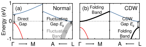
Understanding the the band structure evolution is essential for identifying the origin of the CDW transition [28, 29]. In the normal phase above [Fig. 1(a)], 1T-TiSe2 is a semiconductor with a small indirect gap [28] (or a semimetal with a small band overlap [9]), where the bottom of the conduction band is almost tangent to the Fermi level [30, 31]. Interestingly, there exists a CDW fluctuating band above [14, 7, 8, 32, 33], which may provide a precursor of the CDW gap [34]. In the CDW phase below [Fig. 1(b)], the gap opens by the valence band gradually shifting toward to higher binding energy, leaving the conduction band still tangent to and accompanying with a CDW band folding [15, 8, 9, 16, 32]. Due to the coexistence of the metallic nature and CDW gap in both the normal and CDW phases, the plasmon provides a good window to visualizing the effect of the CDW gap development on the electronic properties. Recently, the plasmon softening at around was proposed to serve as the signature of the EI [21]. However, a recent theoretical study attributed the seemingly plasmon softening signal to the interband transitions [35].
In this letter, using the momentum-resolved high resolution electron energy loss spectroscopy (HREELS) with the capability of two-dimensional energy-momentum mapping [36], we systematically measured the plasmon behaviors in 1T-TiSe2. Our results unambiguously resolve the plasmon from phonon modes and demonstrate the existence of Landau damping [37, 38, 39] to the plasmon at finite momentums within the full temperature range, revealing that there is no plasmon softening at . Extraordinarily, we discover that the plasmon at zero momentum responds to the CDW transition dramatically, from a broad feature covering the energy of meV to a sharp feature with the well-defined resonant frequency at meV in the low-temperature CDW phase. Such a wide-range tunability is attributed to the gap opening associated with the CDW transition that suppresses the interband damping channels of the plasmon.
Temperature-dependent HREELS results. - The measurements were performed on cleaved 1T-TiSe2 single-crystalline samples in situ in a HREELS system with reflected scattering geometry. The detailed experimental methods and sample characterizations are described in the Supplementary Material (SM) [40]. The HREELS data were collected with the sample temperature varying from 35 to 300 K along the two high symmetry directions - and - in the surface Brillouin zone (BZ). The incident electron beam energy from 7 to 110 eV (110 eV data presented in the main paper, while others in the SM [40]) is used , with a typical energy resolution of 3 meV. Figure 2 shows the HREELS results of 1T-TiSe2 at various temperatures. The temperature-dependent E-q// mappings along - and - directions are presented in Figs. 2(a)-(d).
In HREELS, the strong intensity distributions near the point are dominated by the dipole scattering, and the relatively weak features away from the point to the BZ boundary correspond to the impact scattering regime [41]. Then, it is obvious that there are two kinds of distinct energy loss features divided by the energy of 45 meV at 300 K. The loss features higher than 45 meV, labeled as P, are only located near the point, which are pure dipole scattering features and regarded as the plasmon originating from the charge carrier both in the normal and CDW phases [42, 43]. The loss features lower than 45 meV exist throughout the BZ, which are typical impact scattering signals from phonons [41]. To show their dispersions more clearly, Figs. 2(e)-(h) display the second differential images of the original spectra superimposed to the calculated surface phonon dispersions (red lines) using an 11-layer slab model (see the details in the SM [40]). Overall, the calculated phonon dispersions, especially the optical phonon branches, match well with the experimental results.
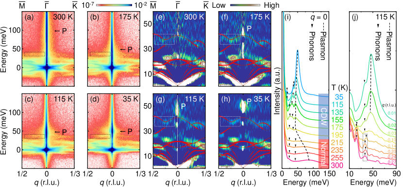
The evolution of the plasmon with temperature is illustrated by a stacking plot of the loss features at the point [Fig. 2(i)]. As the temperature decreases from 300 K to , the energy of the plasmon gets closer to the optical phonon. When the temperature further decreases below , the energy of the plasmon slightly increases and the linewidth of the plasmon changes dramatically. These phenomena will be discussed later in more detail.
Compared to the previous HREELS study in Ref. [21], our results show similar temperature-dependent plasmon behavior at the point, but surprisingly, we did not observe the plasmon softening at . In our energy-momentum mappings at any temperature, the plasmon only exists near the point and does not disperse to the low-energy range at the BZ boundary. In detail, Fig. 2(j) shows dispersion behaviors of the plasmon and phonons in the q space along the - direction 111In the CDW phase, the plasmon line shape is modulated by phonons above 115 K, since the plasmon energy is close to phonons.. The plasmon decays from a sharp peak at q = 0.01 r.l.u. to a weaker peak at q = 0.03 r.l.u. As q increases, the plasmon is not a well-defined peak anymore at r.l.u. and disappears (indistinguishable from noise) beyond q = 0.14 r.l.u. The reported energy loss signal over the entire BZ at 17 K in Ref. [21], interpreted as a dispersionless plasmon, could be from diffusion scattering [41]. In our results, the delicate optical phonon dispersions [those highlighted by the dashed-line rectangles in Fig. 2], which were not observed in Ref. [21], can be clearly resolved from the plasmon. The energy range of these optical phonon branches are close to the claimed softening plasmon energy, so the softening plasmon dispersion around [21] seems from the envelope of phonon signals. Details of the comparison are described in the SM [40].
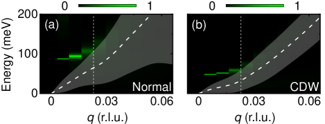
Landau damping of the plasmon. - The observed plasmon damping behaviors can be well understood by the calculations of the loss functions, which were carried in the framework of time-dependent density functional theory (see details in the SM [40]). For simplicity, the calculated band structure in the CDW phase does not include the effects of band folding and renormalization. The calculated single particle excitation (SPE) regions for the normal and CDW band structures are indicated by white dashed line and shadow areas centered at thick white dashed lines in Fig. 3, and plasmon dispersions are represented by color mappings of the calculated loss functions. At the lowest q, plasmons are almost delta functions. However, plasmons broaden and weaken rapidly approaching SPE borders. Beyond the calculated r.l.u. 222The is defined by the minimum of the momentum where there is no zero point in the real part of the calculated dielectric function. See details in the Supplementary Materials [40], plasmons are not well-defined collective excitations anymore due to the strong decay to SPEs. This explains the experimentally observed fast decay of the plasmon at small momentum.
Damping of the plasmon at the long wavelength limit. - Notice there is dramatic change of plasmon behaviors across at the long wavelength limit (near ) , especially the linewidth [Fig. 2(i)]. In the normal state, the relatively broad linewidth indicates the strong plasmon damping above . In contrast, in the CDW state, the linewidth is much smaller, demonstrating that the plasmon damping is largely suppressed below . Moreover, the calculated loss function near is almost a delta function without any damping in Fig. 3 in both the normal and CDW phases, suggesting that an analysis beyond the framework used above (which excludes the CDW band folding) is necessary.
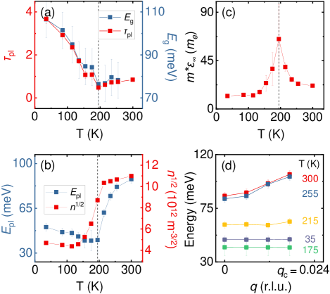
To characterize the temperature-dependent damping behavior at , we plotted the plasmon lifetime parameter in Fig. 4(a), where and are the energy and linewidth of the plasmon, respectively. The damping of the plasmon is slightly enhanced when the temperature decreases from room temperature toward , and as the temperature drops further below , the damping is substantially suppressed, and even becomes much weaker than that at 300 K. Meanwhile, we noticed that the lifetime of the plasmon and the CDW gap as the order parameter (adopted from the resonant inelastic X-ray scattering results [46]) have a synchronous temperature-dependent behavior, implying that the opening of the CDW gap is connected to the enhancement of the plasmon lifetime, that is the depression of the plasmon damping below .
In classical dielectric theory, the effect of the gap (or interband transitions) on plasmons is approximated by the high-frequency dielectric constant , and the plasmon energy or frequency is given by , where , , and are the carrier concentration, the charge of an electron, and the effective electron mass, respectively. In Fig. 4(b), we compared the fitted plasmon energy at from our experiment and the carrier concentration in Ref. [47]. Although both and as functions of temperature show abrupt changes at , the discrepancy between them clearly indicates that, besides the carrier density, there must be other factors that are responsible for the evolution of the plasmon energy. We divided by to exclude the effect of the carrier concentration, and obtained the temperature dependence of the multiplication of and [Fig. 4(c)]. The previous experiment [48] did not show an observable change of near , so the additional drop in plasmon energy compared to on cooling across should be attributed to an abrupt increase in related to the CDW gap. Besides, the plasmon dispersion gradually flattens upon cooling, from a conventional parabolic shape in the normal phase to a dispersionless flat line in the CDW phase, as shown in Fig. 4(d).
Evolution of the plasmon with the CDW gap. - To explain the temperature-dependent plasmon features, we show a phenomenological model where the plasmon evolves with the development of the CDW gap. In this model, we employed a simple dielectric theory to simulate the influence of the interband transition across the CDW gap to the dispersion and damping of the plasmon. The dielectric function can be expressed as follows (see details in the SM [40]):
The first two terms represents a partly screened plasmon by the higher-energy interband transitions other than ones across the CDW gap. In this simulation, the plasmon dispersion follows a parabolic form (yellow lines in Fig. 5) in the random phase approximation. The third term represents the intraband transitions [i.e. the Landau damping in Fig. 3], where corresponds to the SPE boundary 333In this simulation, the interband and intraband transition refer to the SPE boundary, but the SPE continuum in the region of large q is not considered., and is the the linewidth of the intraband transitions. The above parameters in the plasmon and intraband terms are kept constant in this simulation. The last term represents the interband transitions purely originating from the CDW gap (blue lines in Fig. 5), where with the size of the gap, the energy of the conduction band bottom, and C the constant related to the band slope (see details in the SM [40]). is the linewidth of the interband transition across the CDW gap. The loss functions are plotted in Fig. 5 with different CDW gap parameters.
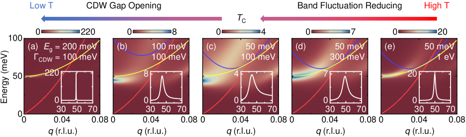
In the normal phase, the lowest interband transition is contributed by the hopping from the CDW fluctuating band [14, 34, 7, 8, 32, 33] to the conduction band at [shown as Fig. 1(a)]. Referring to the resonant inelastic X-ray scattering results [46], we let meV. At high temperature [Fig. 5(e)], the smeared fluctuating band is corresponding to a large eV 444The real may be not so large. To emphasize the evolution of the plasmon, we chose such an extreme value. as a weak damping channel to the plasmon. As the temperature decreases, the band fluctuation becomes smaller, i.e., the fluctuating band tends to be the folding band as a stronger damping channel to the plasmon, which corresponds to the smaller [Figs. 5(c)-(e)]. In this process, the plasmon energy is getting slightly lower, the height is suppressed, and the linewidth broadens. Close to , with meV, the peak of the plasmon becomes asymmetric [Fig. 5(c)], indicating the interference with the interband transition across the CDW gap.
In the CDW phase, the CDW fluctuation changes into a well-defined back-folding band [shown as Fig. 1(b)]. As the temperature decreases, the increases [46, 33] and the interband transitions move away from the plasmon thus reducing the corresponding plasmon damping channel, while the keeps almost constant [Figs. 5(a)-(c)]. In this process, the plasmon energy slightly increases, but more importantly, the plasmon loss feature becomes much more well defined with narrower linewidth compared to the loss feature at high temperature. Besides, the plasmon dispersion becomes close to zero even negative [Fig. 5(b)]. More simulation data with the continuous evolution can be seen in the supplemental video [40].
The drastic changes in the interband transition damping channel responded to the CDW gap evolution result in the anomalous sharping of plasmon feature. Fundamentally, this dramatic response is due to the intrinsic small-gap semiconductor (or semimetal) band structure of the normal phases in 1T-TiSe2, where the interband transitions and the plasmon are close in the energy scale and interfere with each other sensitively [51]. This condition is often not satisfied in regular metal or large-gap semiconductors. This work presents a general framework to understand how the collective electron excitations respond to electron-hole pair excitations in semimetals and small-gap semiconductors and provides possible tunability of plasmons in plasmonic applications [52, 53, 54].
Acknowledgements.
The authors would like to acknowledge Prof. E. W. Plummer for his advises in the initial stage of this study. This work was supported by the National Key R&D Program of China (No. 2021YFA1400200 and No. 2017YFA0303600), the National Natural Science Foundation of China (No. 11874404 and No. 11974399), and the Strategic Priority Research Program of Chinese Academy of Sciences (No. XDB33000000). V. M. S. acknowledges support from the Spanish Ministry of Science and Innovation (Grant No. PID2019–105488GB–I00). X. Z. was partially supported by the Youth Innovation Promotion Association of Chinese Academy of Sciences.References
- Grüner [1988] G. Grüner, Rev. Mod. Phys. 60, 1129 (1988).
- Zhu et al. [2015a] X. Zhu, Y. Cao, J. Zhang, E. W. Plummer, and J. Guo, Proc. Natl. Acad. Sci. U.S.A. 112, 2367 (2015a).
- Di Salvo et al. [1976] F. J. Di Salvo, D. E. Moncton, and J. V. Waszczak, Phys. Rev. B 14, 4321 (1976).
- Hughes [1977] H. P. Hughes, J. Phys. C: Solid State Phys. 10, L319 (1977).
- Wilson [1978] J. A. Wilson, Phys. Status Solidi B: Basic Res. 86, 11 (1978).
- Wakabayashi et al. [1978] N. Wakabayashi, H. Smith, K. Woo, and F. Brown, Solid State Commun. 28, 923 (1978).
- Holt et al. [2001] M. Holt, P. Zschack, H. Hong, M. Y. Chou, and T.-C. Chiang, Phys. Rev. Lett. 86, 3799 (2001).
- Kidd et al. [2002] T. E. Kidd, T. Miller, M. Y. Chou, and T.-C. Chiang, Phys. Rev. Lett. 88, 226402 (2002).
- Rossnagel et al. [2002] K. Rossnagel, L. Kipp, and M. Skibowski, Phys. Rev. B 65, 235101 (2002).
- Weber et al. [2011] F. Weber, S. Rosenkranz, J.-P. Castellan, R. Osborn, G. Karapetrov, R. Hott, R. Heid, K.-P. Bohnen, and A. Alatas, Phys. Rev. Lett. 107, 266401 (2011).
- Hildebrand et al. [2014] B. Hildebrand, C. Didiot, A. M. Novello, G. Monney, A. Scarfato, A. Ubaldini, H. Berger, D. R. Bowler, C. Renner, and P. Aebi, Phys. Rev. Lett. 112, 197001 (2014).
- Porer et al. [2014] M. Porer, U. Leierseder, J. M. Ménard, H. Dachraoui, L. Mouchliadis, I. E. Perakis, U. Heinzmann, J. Demsar, K. Rossnagel, and R. Huber, Nat. Mater. 13, 857 (2014).
- Hildebrand et al. [2016] B. Hildebrand, T. Jaouen, C. Didiot, E. Razzoli, G. Monney, M.-L. Mottas, A. Ubaldini, H. Berger, C. Barreteau, H. Beck, D. R. Bowler, and P. Aebi, Phys. Rev. B 93, 125140 (2016).
- Wilson et al. [1978] J. A. Wilson, A. S. Barker, F. J. D. Salvo, and J. A. Ditzenberger, Phys. Rev. B 18, 2866 (1978).
- Pillo et al. [2000] T. Pillo, J. Hayoz, H. Berger, F. Lévy, L. Schlapbach, and P. Aebi, Phys. Rev. B 61, 16213 (2000).
- Cercellier et al. [2007] H. Cercellier, C. Monney, F. Clerc, C. Battaglia, L. Despont, M. G. Garnier, H. Beck, P. Aebi, L. Patthey, H. Berger, and L. Forró, Phys. Rev. Lett. 99, 146403 (2007).
- Qian et al. [2007] D. Qian, D. Hsieh, L. Wray, E. Morosan, N. L. Wang, Y. Xia, R. J. Cava, and M. Z. Hasan, Phys. Rev. Lett. 98, 117007 (2007).
- Monney et al. [2009] C. Monney, H. Cercellier, F. Clerc, C. Battaglia, E. F. Schwier, C. Didiot, M. G. Garnier, H. Beck, P. Aebi, H. Berger, L. Forró, and L. Patthey, Phys. Rev. B 79, 045116 (2009).
- Monney et al. [2010a] C. Monney, E. F. Schwier, M. G. Garnier, N. Mariotti, C. Didiot, H. Beck, P. Aebi, H. Cercellier, J. Marcus, C. Battaglia, H. Berger, and A. N. Titov, Phys. Rev. B 81, 155104 (2010a).
- Möhr-Vorobeva et al. [2011] E. Möhr-Vorobeva, S. L. Johnson, P. Beaud, U. Staub, R. De Souza, C. Milne, G. Ingold, J. Demsar, H. Schaefer, and A. Titov, Phys. Rev. Lett. 107, 036403 (2011).
- Kogar et al. [2017] A. Kogar, M. S. Rak, S. Vig, A. A. Husain, F. Flicker, Y. I. Joe, L. Venema, G. J. MacDougall, T. C. Chiang, E. Fradkin, J. van Wezel, and P. Abbamonte, Science 358, 1314 (2017).
- van Wezel et al. [2010a] J. van Wezel, P. Nahai-Williamson, and S. S. Saxena, EPL 89, 47004 (2010a).
- van Wezel et al. [2010b] J. van Wezel, P. Nahai-Williamson, and S. S. Saxena, Phys. Rev. B 81, 165109 (2010b).
- van Wezel et al. [2011] J. van Wezel, P. Nahai-Williamson, and S. S. Saxena, Phys. Rev. B 83, 024502 (2011).
- Monney et al. [2011] C. Monney, C. Battaglia, H. Cercellier, P. Aebi, and H. Beck, Phys. Rev. Lett. 106, 106404 (2011).
- May et al. [2011] M. M. May, C. Brabetz, C. Janowitz, and R. Manzke, Phys. Rev. Lett. 107, 176405 (2011).
- Monney et al. [2016] C. Monney, M. Puppin, C. W. Nicholson, M. Hoesch, R. T. Chapman, E. Springate, H. Berger, A. Magrez, C. Cacho, R. Ernstorfer, and M. Wolf, Phys. Rev. B 94, 165165 (2016).
- Monney et al. [2015] G. Monney, C. Monney, B. Hildebrand, P. Aebi, and H. Beck, Phys. Rev. Lett. 114, 086402 (2015).
- Bok et al. [2021] J. M. Bok, J. Hwang, and H.-Y. Choi, Phys. Rev. B 103, 205108 (2021).
- Bianco et al. [2015] R. Bianco, M. Calandra, and F. Mauri, Phys. Rev. B 92, 094107 (2015).
- Wegner et al. [2020] A. Wegner, J. Zhao, J. Li, J. Yang, A. A. Anikin, G. Karapetrov, K. Esfarjani, D. Louca, and U. Chatterjee, Phys. Rev. B 101, 195145 (2020).
- Monney et al. [2012a] C. Monney, G. Monney, P. Aebi, and H. Beck, Phys. Rev. B 85, 235150 (2012a).
- Chen et al. [2016] P. Chen, Y.-H. Chan, X.-Y. Fang, S.-K. Mo, Z. Hussain, A.-V. Fedorov, M. Y. Chou, and T.-C. Chiang, Sci. Rep. 6, 37910 (2016).
- Miyahara et al. [1995] Y. Miyahara, H. Bando, and H. Ozaki, J. Phys. Condens. Matter 7, 2553 (1995).
- Lian et al. [2019] C. Lian, Z. A. Ali, and B. M. Wong, Phys. Rev. B 100, 205423 (2019).
- Zhu et al. [2015b] X. Zhu, Y. Cao, S. Zhang, X. Jia, Q. Guo, F. Yang, L. Zhu, J. Zhang, E. W. Plummer, and J. Guo, Rev. Sci. Instrum. 86, 083902 (2015b).
- Haque and Kliewer [1973] M. S. Haque and K. L. Kliewer, Phys. Rev. B 7, 2416 (1973).
- Pandey et al. [1974] K. Pandey, P. Platzman, P. Eisenberger, and E.-N. Foo, Phys. Rev. B 9, 5046 (1974).
- Raether [2006] H. Raether, Excitation of plasmons and interband transitions by electrons (Springer, 2006).
- [40] See Supplementary Material at http://link.aps.org/. supplementary for details about sample preparation, experimental methods, identifcation of the HREELS features, fitting methods, and calculations, which includes Refs.[55, 56, 57, 58, 59, 60, 61, 62, 63, 64, 65, 66, 67, 68] .
- Ibach and Mills [2013] H. Ibach and D. L. Mills, Electron energy loss spectroscopy and surface vibrations (Academic press, 2013).
- Liang et al. [1979] W. Y. Liang, G. Lucovsky, J. C. Mikkelsen, and R. H. Friend, Philos. Mag. B 39, 133 (1979).
- Li et al. [2007] G. Li, W. Z. Hu, D. Qian, D. Hsieh, M. Z. Hasan, E. Morosan, R. J. Cava, and N. L. Wang, Phys. Rev. Lett. 99, 027404 (2007).
- Note [1] In the CDW phase, the plasmon line shape is modulated by phonons above 115 K, since the plasmon energy is close to phonons.
- Note [2] The is defined by the minimum of the momentum where there is no zero point in the real part of the calculated dielectric function. See details in the Supplementary Materials [40].
- Monney et al. [2012b] C. Monney, K. J. Zhou, H. Cercellier, Z. Vydrova, M. G. Garnier, G. Monney, V. N. Strocov, H. Berger, H. Beck, T. Schmitt, and P. Aebi, Phys. Rev. Lett. 109, 047401 (2012b).
- Knowles et al. [2020] P. Knowles, B. Yang, T. Muramatsu, O. Moulding, J. Buhot, C. J. Sayers, E. Da Como, and S. Friedemann, Phys. Rev. Lett. 124, 167602 (2020).
- Monney et al. [2010b] C. Monney, E. F. Schwier, M. G. Garnier, C. Battaglia, N. Mariotti, C. Didiot, H. Cercellier, J. Marcus, H. Berger, A. N. Titov, H. Beck, and P. Aebi, EPL 92, 47003 (2010b).
- Note [3] In this simulation, the interband and intraband transition refer to the SPE boundary, but the SPE continuum in the region of large q is not considered.
- Note [4] The real may be not so large. To emphasize the evolution of the plasmon, we chose such an extreme value.
- Jensen et al. [1991] E. T. Jensen, R. E. Palmer, W. Allison, and J. F. Annett, Phys. Rev. Lett. 66, 492 (1991).
- Zhu et al. [2016] Z. Zhu, Y. Zou, W. Hu, Y. Li, Y. Gu, B. Cao, N. Guo, L. Wang, J. Song, S. Zhang, H. Gu, and H. Zeng, Adv. Funct. Mater. 26, 1793 (2016).
- Taliercio and Biagioni [2019] T. Taliercio and P. Biagioni, Nanophotonics 8, 949 (2019).
- Cong et al. [2020] S. Cong, X. Liu, Y. Jiang, W. Zhang, and Z. Zhao, The Innovation 1, 100051 (2020).
- Lambin et al. [1990] P. Lambin, J.-P. Vigneron, and A. Lucas, Comput. Phys. Commun. 60, 351 (1990).
- Holy et al. [1977] J. A. Holy, K. C. Woo, M. V. Klein, and F. C. Brown, Phys. Rev. B 16, 3628 (1977).
- Silkin et al. [1984] V. M. Silkin, E. Chulkov, I. Y. Sklyadneva, and V. E. Panin, Sov. Phys. J. 27, 762 (1984).
- Ceperley and Alder [1980] D. M. Ceperley and B. J. Alder, Phys. Rev. Lett. 45, 566 (1980).
- Troullier and Martins [1991] N. Troullier and J. L. Martins, Phys. Rev. B 43, 1993 (1991).
- Rohwer et al. [2011] T. Rohwer, S. Hellmann, M. Wiesenmayer, C. Sohrt, A. Stange, B. Slomski, A. Carr, Y. Liu, L. M. Avila, M. Kalläne, S. Mathias, L. Kipp, K. Rossnagel, and M. Bauer, Nature 471, 490 (2011).
- Pines and Philippe [1966] D. Pines and N. Philippe, Theory of Quantum Liquids: Normal Fermi Liquids (1st ed.) (CRC Press, 1966).
- Runge and Gross [1984] E. Runge and E. K. U. Gross, Phys. Rev. Lett. 52, 997 (1984).
- Petersilka et al. [1996] M. Petersilka, U. J. Gossmann, and E. K. U. Gross, Phys. Rev. Lett. 76, 1212 (1996).
- Silkin et al. [2003] V. M. Silkin, E. V. Chulkov, and P. M. Echenique, Phys. Rev. B 68, 205106 (2003).
- Kresse and Furthmüller [1996] G. Kresse and J. Furthmüller, Phys. Rev. B 54, 11169 (1996).
- Togo and Tanaka [2015] A. Togo and I. Tanaka, Scr. Mater. 108, 1 (2015).
- Powell [1969] C. J. Powell, J. Opt. Soc. Am. 59, 738 (1969).
- Drube et al. [1984] W. Drube, I. Schäfer, G. Karschnick, and M. Skibowski, Phys. Rev. B 30, 6248 (1984).