Probing the optical near-field interaction of Mie nanoresonators
with atomically thin semiconductors
Abstract
Optical Mie resonators based on silicon nanostructures allow tuning of light-matter-interaction with advanced design concepts based on CMOS compatible nanofabrication. Optically active materials such as transition-metal dichalcogenide (TMD) monolayers can be placed in the near-field region of such Mie resonators. Here, we experimentally demonstrate and verify by numerical simulations coupling between a MoSe2 monolayer and the near-field of dielectric nanoresonators. Through a comparison of dark-field (DF) scattering spectroscopy and photoluminescence excitation experiments (PLE), we show that the MoSe2 absorption can be enhanced via the near-field of a nanoresonator. We demonstrate spectral tuning of the absorption via the geometry of individual Mie resonators. We show that we indeed access the optical near-field of the nanoresonators, by measuring a spectral shift between the typical near-field resonances in PLE compared to the far-field resonances in DF scattering. Our results prove that using MoSe2 as an active probe allows accessing the optical near-field above photonic nanostructures, without the requirement of highly complex near-field microscopy equipment.
Introduction.— Optical resonators are essential in many applications such as laser systems and sensing. The physical size and properties of the resonator are adapted to the specific application and to the relevant part of the electromagnetic spectrum novotny2012principles . Optical resonators that are capable of amplifying optical fields in very small nanoscopic volumes, for addressing individual nanocrystals or molecules in the near-field, are called nanoresonators kleemann2017strong ; petric2022tuning ; liu2016strong ; zhou2017probing ; sortino2019enhanced ; bidault2019dielectric ; mupparapu2020integration ; brongersma2021road ; chen2017enhanced ; bucher2019tailoring ; cihan2018silicon ; shinomiya2022enhanced . They can be fabricated by bottom-up techniques, such as growth of metallic nanoparticles, or top-down approaches, such as Si-nanoresonators on CMOS compatible substrates zhao2009mie ; wiechaEvolutionaryMultiobjectiveOptimization2017 ; won2019into ; gonzalez2021scaling ; kuznetsov2016optically ; kallelPhotoluminescenceEnhancementSilicon2013 .
Whereas the resonance energies of a resonator with macroscopic dimensions, such as a laser cavity, are directly accessible in a standard optical far-field measurement, the situation for nanoresonators is more challenging.
It has been shown experimentally and in a substantial body of theory work that there is a shift between the optical resonance energy in the near-field compared to the measured resonance energies in the far-field. The exact near-field resonance is key for applications for example in sensing of molecules directly placed in the near-field chen2019modern and it has been accessed up to now either in sophisticated tip-enhanced experiments or through extrapolation from far-field data messingerLocalFieldsSurface1981 ; rossComparisonFarfieldMeasures2009 ; katsEffectRadiationDamping2011 ; zuloagaEnergyShiftNearField2011 ; alonso-gonzalezExperimentalVerificationSpectral2013 .
Here we show that by placing an atomically thin semiconductor directly in the near-field of individual dielectric nanoresonators, we have access to the near-field resonance energies without the use of complex near-field spectroscopy techniques. We compare the near-field resonance energies with far-field resonance energy measurements on the same resonators and observe a clear blue-shift of the near-field energies in our far-field results. We show tuning of the optical absorption of the atomically thin semiconductor MoSe2 through the interaction with the nanoresonator near-field and our results are well reproduced by model calculations of the shift between near-and far-field resonances.
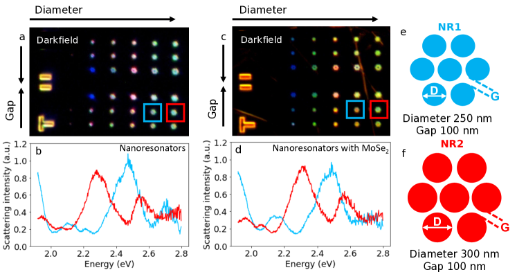
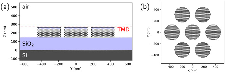
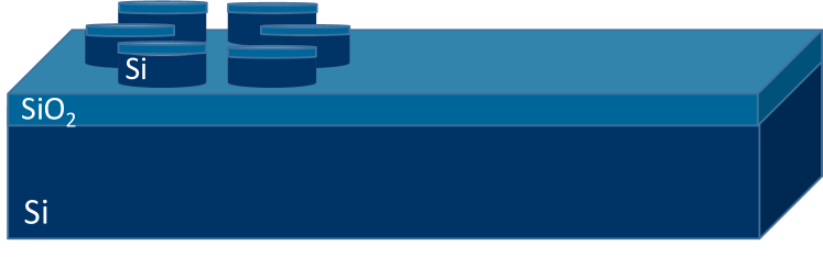
Results and Discussion.— We fabricated two sets of Si/SiO2 nanoresonator arrays on silicon-on-insulator (SOI) substrates. The nanoresonators are cylindrical pillars, arranged as close-packed heptamers as sketched in Fig. 1e and 1f. The diameters of the individual cylinders increase from 50 nm to 300 nm with steps of 50 nm. The gaps between neighbouring pillars are 50 nm, 100 nm or 300 nm. The structures are fabricated as arrays of seven discs to match approximately the size of a diffraction limited, focused laser beam, in order to maximize the experimental signal associated with the Si-NRs. On the final nanostructures, MoSe2 monolayers are aligned and transferred on top of the nanoresonators using a micromanipulator system castellanos2014deterministic . A description of the fabrication process is given in the supporting information.
In figure 1a we show dark-field (DF) images of the nanoresonators before MoSe2 transfer, figure 1c shows the same sample after transfer of an MoSe2 monolayer flake. A bright-field microscope image of the nanoresonators after MoSe2 deposition is shown in the supplement Fig. S3, where the MoSe2 covered region is clearly visible. By varying the Si-NR gap and diameter, different colors appear in the DF images, which demonstrates the geometry-dependent Mie resonance energy shifts of the individual resonators in the visible spectral range.
DF spectra are collected using the same setup as the DF images. To this end, the signal is sent to a spectrometer instead of the imaging camera. The setup for taking dark-field images and spectra is depicted in the supplement Fig. 4.
We will focus in the following on two selected nanoresonators, “NR1” (blue, Fig. 1e) and “NR2” (red, Fig. 1f). These heptamers have respective diameters of 250 nm (NR1) and 300 nm (NR2), the gap between the pillars is identical for both Si-NRs (100 nm).
We selected these two NRs because their main Mie resonances lie at different, well distinguishable energies.
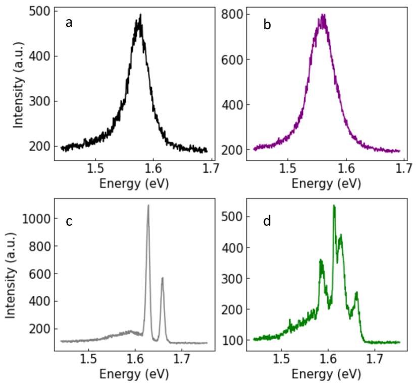
We measured the scattered light intensity before and after the monolayer transfer, shown in Fig. 1b, respectively 1d.
We observed a small, global blue-shift on the order of 10 meV for the resonances when the MoSe2 monolayer was on top of the nanoresonators, this small energy-shift is at the limit of our detection accuracy. Knowing the size of this shift is helpful for analyzing the spectral shift between measured near-field and far-field resonances discussed below.
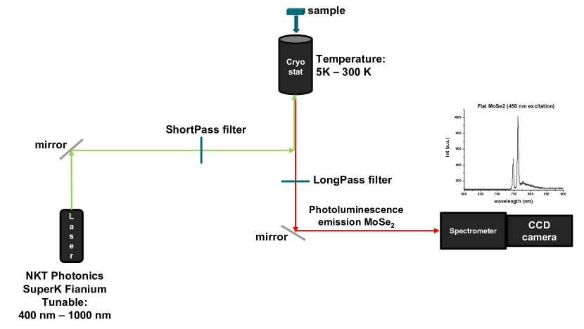
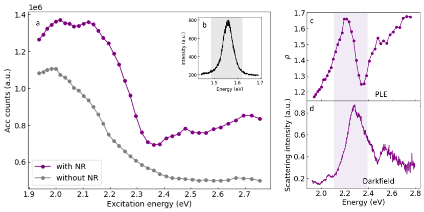
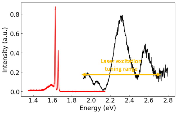
Spectral shift between near-field and far-field. In a second step, we want to analyze the impact of the nanoresonators on the absorption of the MoSe2 monolayer. We carry out photoluminescence excitation (PLE) experiments shree2021guide where temperature, position, and optical power are kept constant and the excitation wavelength is varied from 450 nm to 650 nm (corresponding to 2.75 eV - 1.90 eV). The optical power of the laser is set to 100 nW, after making sure that the MoSe2 absorption is not saturated at this illumination power (see also supplemental figure S4). We avoid tuning the laser close to the MoSe2 exciton emission peaks which occur around 745 nm (eV)vanderzandeGrainsGrainBoundaries2013 ; cadizUltralowPowerThreshold2016 ; wang2015exciton , in order to remain in a non-resonant excitation regime. During the entire measurements, the sample is kept in a closed-loop cryostat at a temperature of 5 K. Typical PL spectra are shown in the supplemental Fig. 9, where we also provide a comparison with room temperature measurements ( K). An illustration of the optical setup can also be found in the SI Fig. 5.
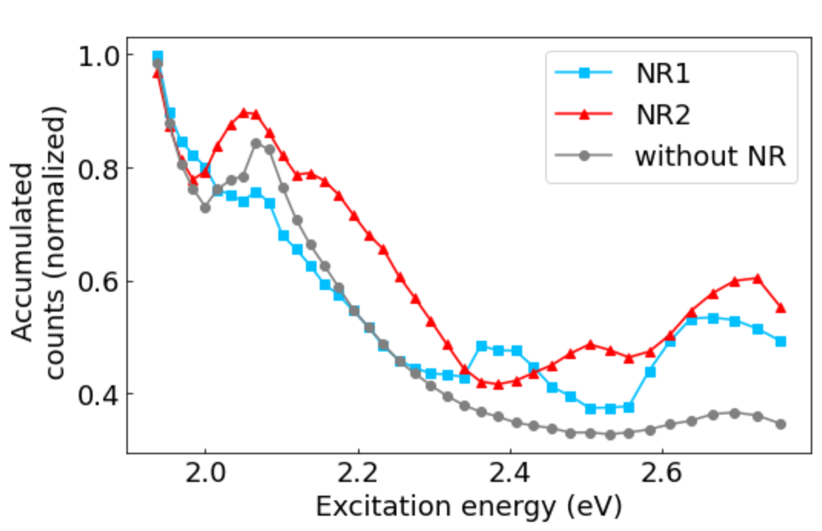
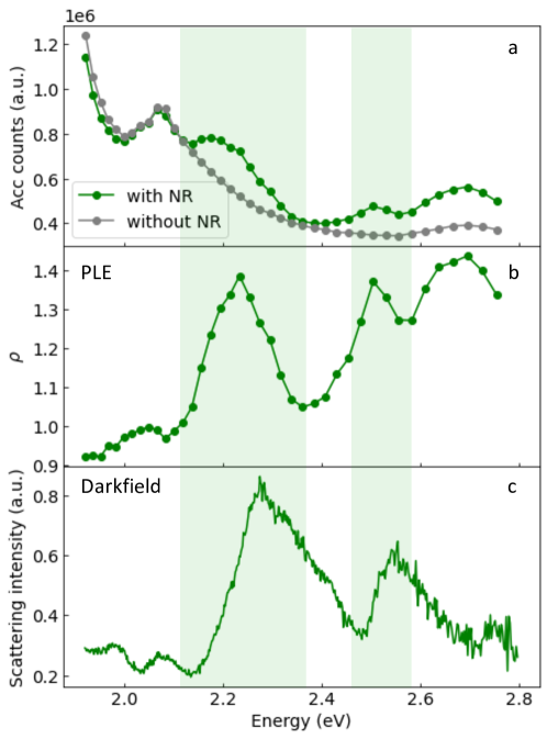
The absorption and hence the PLE response of the bare MoSe2 shree2021guide is expected to vary with the excitation energy. This variation is a result of the material’s band-structure, the presence of high energy excitonic states as well as coupling to phonons chow2017phonon ; wang2015exciton ; kozawa2016evidence ; shree2018observation . Our goal is to investigate how the absorption is modified by Mie resonances of the Si-NRs. To distinguish effects induced by Mie-resonances from material-related variations in the bare MoSe2, we compare PLE measurements from MoSe2 monolayers lying on the flat substrate with MoSe2 on top of the nanoresonators. This is shown in Fig. 2 for NR1 and NR2. The PL emission spectra for each excitation laser wavelength are numerically integrated, by summation of the counts per second in the spectral range around the emission peaks, from 1.5 eV - 1.7 eV (see SI for raw spectra) atkinson1989introduction . Hence, each data point in Fig. 2 is a separate PL measurement for a specific laser excitation energy. The direct comparison of the PLE measurements from MoSe2 with and without Si-NR (c.f. Fig. 2), already reveals clear differences. To better visualize the effect of the nanoresonators on the PLE signal, we divide the integrated PL intensities from MoSe2 on the Si-NRs (blue squares and red triangles in Fig. 2) by the signal from the bare MoSe2 (on flat substrate, gray dotted line in Fig. 2):
| (1) |
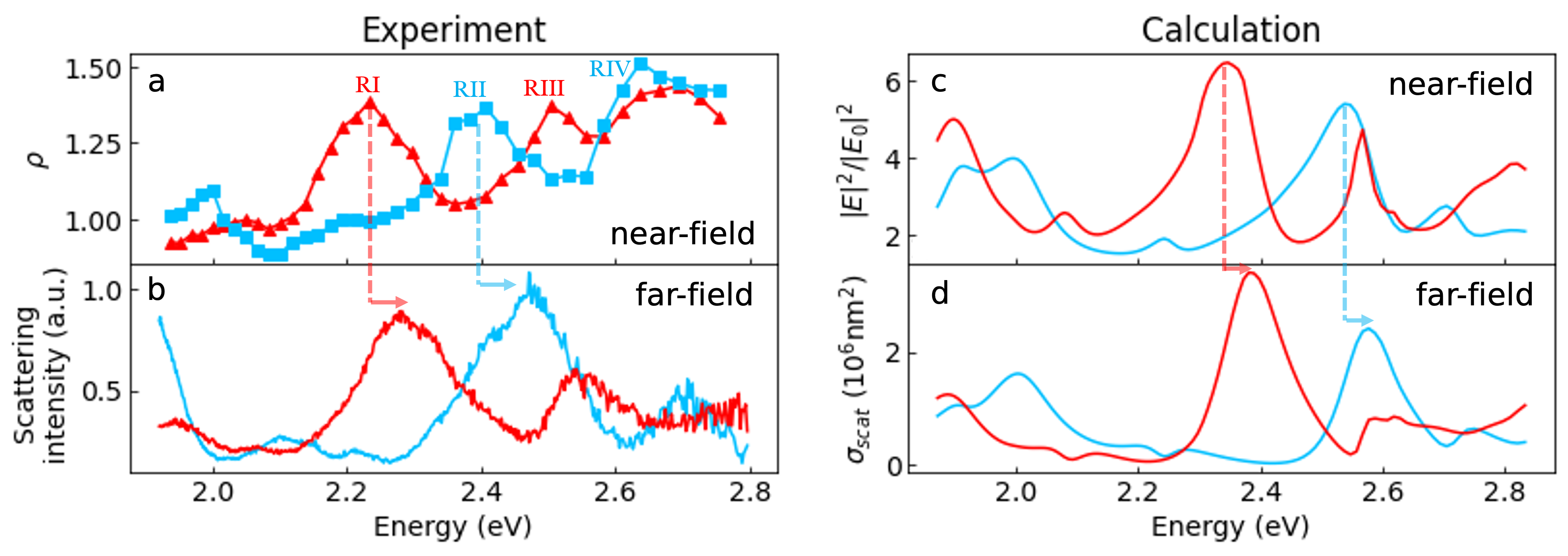
This ratio gives an estimation of the absorption enhancement due to the presence of a nanoresonator supporting Mie resonances. The Mie resonances locally amplify the optical near-field, enhancing absorption in the monolayer which leads after carrier relaxation to a stronger PL emission. Spectra of as a function of the excitation energy are shown in Fig. 3a. In order to show spectral tuning of the absorption enhanced by Mie-resonances we perform experiments on the two nanoresonators NR1 and NR2 (see Fig. 1e and f). We find that their main resonances (labelled RI, …, RIV) occur at well separated energies (see table 1 for values). Around the main Mie resonances we observe a PL emission enhancement of about 1.44. A comparison with the DF scattering spectrum (Fig. 3b) shows, that the PLE maxima are governed by the Mie-resonances. The spectral shifts between NR1 and NR2 are consistent between near- and far-field measurements. This is a clear signature that the MoSe2 monolayer is coupled to the optical near-field above the Si-NR in the regime of weak coupling.
| RI (eV) | RII (eV) | RIII (eV) | RIV (eV) | |
|---|---|---|---|---|
| PLE | 2.23 | 2.41 | 2.50 | 2.64 |
| dark-field | 2.28 | 2.46 | 2.54 | 2.71 |
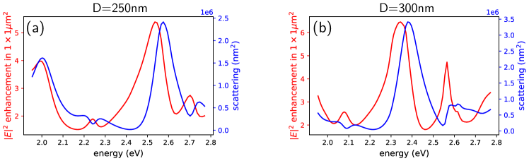
Theoretical simulations : We compare the experimental PLE spectra to full-field simulations via the Green’s dyadic method (GDM) using our own python implementation “pyGDM” wiecha2018pygdm ; wiechaPyGDMNewFunctionalities2022 . The GDM is a volume discretization approach to solve Maxwell’s equations in the frequency domain girardFieldsNanostructures2005 . A nanostructure of arbitrary shape and material is discretized on a regular hexagonal compact grid. We use tabulated refractive indices from literature for both parts of the pillars, the first 95 nm consisting of silicon edwardsSiliconSi1997 while the 30 nm thick capping is made of SiO2 malitsonInterspecimenComparisonRefractive1965 . With according Green’s tensors paulusAccurateEfficientComputation2000 , we describe the layered substrate, where a bulk silicon substrate is followed by a SiO2 spacer layer of 145 nm, on top of which the nano-structures are placed in air. We illuminate the system with a plane wave at normal incidence in the same wavelength range as used in the experiments and we incoherently average two orthogonal linear polarizations. We calculate the electric field intensity enhancement just above the SiO2 capping on the Si pillars in an area of µm2, corresponding approximately to the size of the focused Gaussian laser beam ( emission beam diameter). Sketches and more details about simulations and model geometry can be found in the SI.
The simulated spectra of the average near-field enhancement above the top surface are shown in Fig. 2c for heptamers with pillar diameters of nm (NR1, blue) and nm (NR2, red), and the far-field scattered intensity for the same structures shown in Fig. 2d. We observe a good agreement with the experimental data, the simulations reproduce in particular all major resonance features. Very importantly our simulations reproduce the red-shift of the resonances when the structure size increases from nm to nm and the near-to far-field shift. Please note that the systematic blue-shift of around eV between the absolute values of the simulated resonances and the experiment can be explained by the rough discretization of the Si discs’ circular cross-sections on a coarse, regular mesh. Also, inaccuracies of the fabricated sample dimensions may play a role, in fact, deviations in the order of - nm between design and actual sample would induce an according systematic shift patoux2021challenges .
Discussion : The comparison of the far-field DF scattering spectra with the MoSe2 PLE spectra clearly demonstrate, that the Mie resonances of high-index dielectric nanoresonators can be used to tailor the absorption of a TMD layer. Furthermore, our results show that the PLE measurements access the optical near-field and probe the local field intensity enhancement. In the lateral directions (parallel to the substrate plane) the measurements reflect the average near-field intensity in a large zone, corresponding approximately to the illuminated area. Perpendicular to the surface on the other hand, the local near-field is probed in an extremely narrow vertical region, because the TMD is atomically thin.
An unambiguous proof that we do indeed probe the optical near-field with the PLE technique is provided by the observation of a systematic shift between near-field spectra (PLE) and far-field measurements (DF scattering). This shift is of the order of meV (see also Table 1) and is reproduced by our simulations (Fig. 3c and d). It corresponds to the widely studied resonance shift between far-field and near-field, where the near-field amplitude is shifted to lower energies, compared to the far-field response. To get an intuitive, qualitative understanding, this shift can be explained with a damped harmonic oscillator (HO) model. The HO amplitude is given by:
| (2) |
where is the driving amplitude, in our case corresponding the amplitude of the incident field. Solving Eq. (2) for its extrema, one finds easily that the damping term leads to a red-shift of the maximum resonator amplitude with respect to the eigenfrequency zuloagaEnergyShiftNearField2011 :
| (3) |
On the other hand, far-field observables like the scattering or extinction cross section are proportional to the oscillator’s kinetic energy, whose time average can be shown to be maximum at the non-shifted eigenfrequency zuloagaEnergyShiftNearField2011 . While the effect has first been discussed for lossy plasmonic nanoresonantors messingerLocalFieldsSurface1981 , it has been explicitly shown later that radiative damping, responsible for broadening of leaky Mie resonances like in our SiNRs, leads to an analogous near-field shift zuloagaEnergyShiftNearField2011 . The shift has been experimentally demonstrated on plasmonic structures via scanning near-field microscopy (SNOM) measurements alonso-gonzalezExperimentalVerificationSpectral2013 .
Without complex SNOM equipment, here we experimentally observe a red-shift of the PLE spectra compared to the far-field scattering results. It is in the order of the shift predicted by our near-field enhancement simulations, and therefore a clear signature that we indeed probe the optical near-field of the silicon nanostructures.
These observations rely on a sufficient spectral resolution to observe the near-field red-shift in the PLE data. Please note that our approach also works at room temperature, as shown in the SI Fig. 8.
In conclusion, we transferred monolayers of MoSe2 on top of Mie resonant silicon nanostructure arrays and compared the far-field scattering of these scatterers, using DF spectroscopy, with spectrally resolved measurements of photoluminescence enhancement. The latter is probing the optical near-field at the location of the TMD monolayer, i.e. just above the silicon nanostructures. We found that the PLE spectra show the same resonant features as the far-field measurements. We also observe the typical near-to-far-field spectral shift between the two types of measurements, which unambiguously confirms that we have access to the optical near-field of the silicon nanostructures. All results are confirmed by numerical full-field simulations. Our results demonstrate that the absorption efficiency and consequently the emission of direct-bandgap monolayer semiconductors can be enhanced and spectrally tuned by placing optically resonant nano-structures in their vicinity. It furthermore proves that the PLE measurements provide access to the optical near-field in an extremely narrow vertical region in the order of a nanometer (thickness of the TMD monolayer). Our work offers important insights for the design of efficient TMD-based nano-devices for light detection and emission.
Methods.— The silicon pillars were fabricated in a top-down approach via electron-beam lithography (EBL) and subsequent anisotropic plasma etching han_realization_2011 ; guerfi_high_2013 . Monolayer MoSe2 flakes are exfoliated from bulk 2H-MoSe2 crystals on Nitto Denko tape novoselov2005two and then exfoliated again on a polydimethylsiloxane (PDMS) stamp placed on a glass slide for inspection under the optical microscope, see supplement for further details.
I Supplement
I.1 Nano-structure fabrication and TMD exfoliation
The silicon pillars were fabricated in a top-down approach via electron-beam lithography (EBL) and subsequent anisotropic plasma etching han_realization_2011 ; guerfi_high_2013 . A negative-tone resist (hydrogen silsesquioxane, HSQ) was spin-coated as thin film (around 50nm) on a commercial silicon-on-insulator (SOI) substrate. The SOI consists of bulk silicon followed by a 145nm thick burried oxide layer made of SiO2 (BOX). On top of the BOX follows a 95nm high silicon overlayer, which serves as building material for the nano-structures. The nano-patterns were written in the HSQ resist using a RAITH 150 writer at an energy of 30 keV. After EBL exposure, the resist was developed in % tetramethylammonium hydroxide (TMAH). Finally, the patterns were etched into the 95nm thick silicon overlayer via reactive ion etching (RIE) in a SF6/C4F8 plasma. RIE was stopped once etching arrived at the BOX layer. After the processing, an additional SiO2 layer of approximately 30nm height remains on top of the structured Si, which is the residual developped HSQ resist.
Monolayer MoSe2 flakes are exfoliated from bulk 2H-MoSe2 crystals on Nitto Denko tape novoselov2005two and then exfoliated again on a polydimethylsiloxane (PDMS) stamp placed on a glass slide for inspection under the optical microscope. Prior to transfer of MoSe2 monolayers, the substrate with the nanoresonators is wet-cleaned by 60 s ultrasonication in acetone and isopropanol and exposed to oxygen-assisted plasma.
I.2 Power Dependence of PL intensity
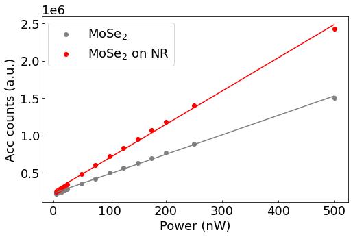
To evaluate the enhancement we also carried out power dependent experiments. We keep temperature, position, and excitation wavelength fixed, and now we vary the optical power from 10 - 500 nW (see SI Fig. S4). The enhancement we measure in emission (on the NRs as compared to next to them) is a lower bound for the enhancement in absorption as the generated excitons do not all recombine radiatively (i.e. by emitting a photon in our detection window) shin2014photoluminescence ; kumar2014exciton ; zhang2021defect ; han2018exciton .
I.3 Simulations details
Data availability statement : The data that support the findings of this study are available from the corresponding authors upon request.
Acknowledgements : We acknowledge partial funding from ANR HiLight, NanoX project 2DLight, the Institute of quantum technology in Occitanie IQO and a UPS excellence PhD grant. This work was supported by the Toulouse HPC CALMIP (grant p20010), and by the LAAS-CNRS micro and nanotechnologies platform, a member of the French RENATECH network. IP acknowledges financial support by the Hellenic Foundation for Research and Innovation (H.F.R.I.) under the “3rd Call for H.F.R.I. Research Projects to support Post-Doctoral Researchers” (Project Number: 7898).
Author contributions : V.L. fabricated the high quality Si-SiO2 starting structure. J.M. and G.L. fabricated the nanoresonators based on the design of A.C.,G.A. and V.P. A.E-R. and I.P. deposited the TMD layer on the nanoresonators. A.E-R., P.R.W. and J-M.P. performed dark-field experiments that were analyzed with all co-authors. D.L. and X.M. mounted the laser system for PLE. A.E-R. performed PLE and analyzed data with I.P. P.R.W., A.E-R., A.G. and A.C. performed modelling of the resonances. A.E-R. wrote the manuscript with input from all co-authors. V.P., G.L., P.R.W. and B.U. supervised the project.
Competing interests : The authors declare no competing interests.
References
- (1) Novotny, L. & Hecht, B. Principles of nano-optics (Cambridge university press, 2012).
- (2) Kleemann, M.-E. et al. Strong-coupling of wse2 in ultra-compact plasmonic nanocavities at room temperature. Nature communications 8, 1–7 (2017).
- (3) Petric, M. M. et al. Tuning the optical properties of a mose2 monolayer using nanoscale plasmonic antennas. Nano Letters 22, 561–569 (2022).
- (4) Liu, W. et al. Strong exciton–plasmon coupling in mos2 coupled with plasmonic lattice. Nano letters 16, 1262–1269 (2016).
- (5) Zhou, Y. et al. Probing dark excitons in atomically thin semiconductors via near-field coupling to surface plasmon polaritons. Nature nanotechnology 12, 856–860 (2017).
- (6) Sortino, L. et al. Enhanced light-matter interaction in an atomically thin semiconductor coupled with dielectric nano-antennas. Nature communications 10, 1–8 (2019).
- (7) Bidault, S., Mivelle, M. & Bonod, N. Dielectric nanoantennas to manipulate solid-state light emission. Journal of Applied Physics 126, 094104 (2019).
- (8) Mupparapu, R., Bucher, T. & Staude, I. Integration of two-dimensional transition metal dichalcogenides with mie-resonant dielectric nanostructures. Advances in Physics: X 5, 1734083 (2020).
- (9) Brongersma, M. L. The road to atomically thin metasurface optics. Nanophotonics 10, 643–654 (2021).
- (10) Chen, H. et al. Enhanced directional emission from monolayer wse2 integrated onto a multiresonant silicon-based photonic structure. ACS Photonics 4, 3031–3038 (2017).
- (11) Bucher, T. et al. Tailoring photoluminescence from mos2 monolayers by mie-resonant metasurfaces. ACS Photonics 6, 1002–1009 (2019).
- (12) Cihan, A. F., Curto, A. G., Raza, S., Kik, P. G. & Brongersma, M. L. Silicon mie resonators for highly directional light emission from monolayer mos2. Nature Photonics 12, 284–290 (2018).
- (13) Shinomiya, H. et al. Enhanced light emission from monolayer mos2 by doubly resonant spherical si nanoantennas. ACS Photonics (2022).
- (14) Zhao, Q., Zhou, J., Zhang, F. & Lippens, D. Mie resonance-based dielectric metamaterials. Materials today 12, 60–69 (2009).
- (15) Wiecha, P. R. et al. Evolutionary multi-objective optimization of colour pixels based on dielectric nanoantennas. Nature Nanotechnology 12, 163–169 (2017).
- (16) Won, R. Into the ’mie-tronic’ era. Nature Photonics 13, 585–587 (2019).
- (17) Gonzalez-Zalba, M. et al. Scaling silicon-based quantum computing using cmos technology. Nature Electronics 4, 872–884 (2021).
- (18) Kuznetsov, A. I., Miroshnichenko, A. E., Brongersma, M. L., Kivshar, Y. S. & Luk’yanchuk, B. Optically resonant dielectric nanostructures. Science 354, aag2472 (2016).
- (19) Kallel, H. et al. Photoluminescence enhancement of silicon nanocrystals placed in the near field of a silicon nanowire. Physical Review B 88, 081302 (2013).
- (20) Chen, X. et al. Modern scattering-type scanning near-field optical microscopy for advanced material research. Advanced Materials 31, 1804774 (2019).
- (21) Messinger, B. J., von Raben, K. U., Chang, R. K. & Barber, P. W. Local fields at the surface of noble-metal microspheres. Physical Review B 24, 649–657 (1981).
- (22) Ross, B. M. & Lee, L. P. Comparison of near- and far-field measures for plasmon resonance of metallic nanoparticles. Optics Letters 34, 896–898 (2009).
- (23) Kats, M. A., Yu, N., Genevet, P., Gaburro, Z. & Capasso, F. Effect of radiation damping on the spectral response of plasmonic components. Optics Express 19, 21748–21753 (2011).
- (24) Zuloaga, J. & Nordlander, P. On the Energy Shift between Near-Field and Far-Field Peak Intensities in Localized Plasmon Systems. Nano Letters 11, 1280–1283 (2011).
- (25) Alonso-González, P. et al. Experimental Verification of the Spectral Shift between Near- and Far-Field Peak Intensities of Plasmonic Infrared Nanoantennas. Physical Review Letters 110, 203902 (2013).
- (26) Castellanos-Gomez, A. et al. Deterministic transfer of two-dimensional materials by all-dry viscoelastic stamping. 2D Materials 1, 011002 (2014).
- (27) Shree, S., Paradisanos, I., Marie, X., Robert, C. & Urbaszek, B. Guide to optical spectroscopy of layered semiconductors. Nature Reviews Physics 3, 39–54 (2021).
- (28) van der Zande, A. M. et al. Grains and grain boundaries in highly crystalline monolayer molybdenum disulphide. Nature Materials 12, 554–561 (2013).
- (29) Cadiz, F. et al. Ultra-low power threshold for laser induced changes in optical properties of 2D molybdenum dichalcogenides. 2D Materials 3, 045008 (2016).
- (30) Wang, G. et al. Exciton states in monolayer mose2: impact on interband transitions. 2D Materials 2, 045005 (2015).
- (31) Chow, C. M. et al. Phonon-assisted oscillatory exciton dynamics in monolayer mose2. npj 2D Materials and Applications 1, 1–6 (2017).
- (32) Kozawa, D. et al. Evidence for fast interlayer energy transfer in mose2/ws2 heterostructures. Nano letters 16, 4087–4093 (2016).
- (33) Shree, S. et al. Observation of exciton-phonon coupling in mose 2 monolayers. Physical Review B 98, 035302 (2018).
- (34) Atkinson, K. E. An introduction to numerical analysis. new york: John willey & sons (1989).
- (35) Wiecha, P. R. pygdm - a python toolkit for full-field electro-dynamical simulations and evolutionary optimization of nanostructures. Computer Physics Communications 233, 167–192 (2018).
- (36) Wiecha, P. R. et al. pyGDM - new functionalities and major improvements to the python toolkit for nano-optics full-field simulations. Computer Physics Communications 270, 108142 (2022).
- (37) Girard, C. Near fields in nanostructures. Reports on Progress in Physics 68, 1883–1933 (2005).
- (38) Edwards, D. F. Silicon (Si)*. In Palik, E. D. (ed.) Handbook of Optical Constants of Solids, 547–569 (Academic Press, Burlington, 1997).
- (39) Malitson, I. H. Interspecimen Comparison of the Refractive Index of Fused Silica. Journal of the Optical Society of America 55, 1205 (1965).
- (40) Paulus, M., Gay-Balmaz, P. & Martin, O. J. F. Accurate and efficient computation of the Green’s tensor for stratified media. Physical Review E 62, 5797–5807 (2000).
- (41) Patoux, A. et al. Challenges in nanofabrication for efficient optical metasurfaces. Scientific reports 11, 1–12 (2021).
- (42) Han, X.-L., Larrieu, G., Fazzini, P.-F. & Dubois, E. Realization of ultra dense arrays of vertical silicon nanowires with defect free surface and perfect anisotropy using a top-down approach. Microelectronic Engineering 88, 2622–2624 (2011). URL http://www.sciencedirect.com/science/article/pii/S0167931710005903.
- (43) Guerfi, Y., Carcenac, F. & Larrieu, G. High resolution HSQ nanopillar arrays with low energy electron beam lithography. Microelectronic Engineering 110, 173–176 (2013). URL http://www.sciencedirect.com/science/article/pii/S0167931713002724.
- (44) Novoselov, K. S. et al. Two-dimensional atomic crystals. Proceedings of the National Academy of Sciences 102, 10451–10453 (2005).
- (45) Shin, M. J., Kim, D. H. & Lim, D. Photoluminescence saturation and exciton decay dynamics in transition metal dichalcogenide monolayers. Journal of the Korean Physical Society 65, 2077–2081 (2014).
- (46) Kumar, N. et al. Exciton-exciton annihilation in mose 2 monolayers. Physical Review B 89, 125427 (2014).
- (47) Zhang, T. & Wang, J. Defect-enhanced exciton–exciton annihilation in monolayer transition metal dichalcogenides at high exciton densities. ACS Photonics 8, 2770–2780 (2021).
- (48) Han, B. et al. Exciton states in monolayer mose 2 and mote 2 probed by upconversion spectroscopy. Physical Review X 8, 031073 (2018).