Hidden Symmetry Protection and Topology in Surface Maxwell Waves
Abstract
Since the latter half of the 20th century, the use of metal in optics has become a promising plasmonics field for controlling light at a deep subwavelength scale. Surface plasmon polaritons localized on metal surfaces are crucial in plasmonics. However, despite the long history of plasmonics, the underlying mechanism producing the surface waves is not fully understood. This study unveils the hidden symmetry protection that ensures the existence of degenerated electric zero modes. These zero modes are identified as physical origins of surface plasmon polaritons, and similar zero modes can be directly excited at a temporal boundary. In real space, the zero modes possess vector-field rotation related to surface impedance. Focusing on the surface impedance, we prove the bulk–edge correspondence, which guarantees the existence of surface plasmon polaritons even with nonuniformity. Lastly, we extract the underlying physics in the topological transition between metal and dielectric material using a minimal circuit model with duality. The transition is considered the crossover between electric and magnetic zero modes.
I Introduction
Metal has been one of the fundamental materials for producing optical elements, such as mirrors, for over 5000 years [1]. However, despite its extensive history, wave propagation inside metals has received little attention, because electromagnetic waves are attenuated in metals owing to their negative response. Because free electrons in a metal are sensitive to oscillating electric fields, the electric field and induced current have opposite phases. Since the 20th century, researchers have investigated extraordinary light propagation enabled by a negative response. One prominent example is the discovery of a negative refractive index, which can be realized in a medium with simultaneous negative responses for electric and magnetic fields [2]. Remarkably, a negative refractive index can be applied to realize a flat lens, which can help overcome the diffraction limit [3]. Because there is no natural material with a negative refractive index, the discovery stimulated the development of artificial materials called metamaterials [4, 5], and negative refraction was eventually demonstrated in a metamaterial [6]. These findings demonstrate the potential capability of the negative response in optics.
The negative response impacts not only spatial wave propagation but also surface-wave formation. In fact, a metallic surface supports surface plasmon polaritons, i.e., hybridized waves comprising a plasmonic electron oscillation and an electromagnetic wave [7, 8]. As surface plasmon polaritons can be squeezed into a deep subwavelength volume, they play essential roles in nanophotonics toward the miniaturization of optics, and the research field involving surface plasmon polaritons is called plasmonics [9]. Although surface plasmon polaritons have been studied for over half a century, the investigation of their origin only began recently. In the paradigm of topological physics, integers are used to characterize bulk materials, where the bulk–edge correspondence predicts the existence of a boundary mode between two materials with different topological numbers [10, 11]. The bulk–edge correspondence provides a powerful guiding principle; however, it is often empirical and requires exact proof for each case. For plasmonic systems, different integers are used to distinguish between a metal and dielectric material, such as the number describing the winding of the complex helicity spectrum [12] and the Zak phase [13]. The existence of surface plasmon polaritons is indicated by the bulk–edge correspondence. However, these seminal works are limited to simply observing surface-wave formations and lack rigorous proof of the bulk–edge correspondence.
In this study, special zero modes were identified as the origin of surface Maxwell waves, and a general bulk–edge correspondence is rigorously established that explained the existence of surface plasmon polaritons on metals. The first approach is based on symmetry protection. It guarantees the existence of localized states under certain symmetry. In Sec. II, we formulate symmetry-protected electric zero modes in electrostatics, which are the origin of surface plasmon polaritons. The robustness of symmetry protection in some nonuniform systems is confirmed. Additionally, we demonstrate that analogous zero modes can be experimentally excited at a temporal boundary. In Sec. III, we investigate real-space topological polarization rotation in the electric zero modes. Keller–Dykhne self-duality is identified as the physical origin of polarization rotation. Furthermore, we reveal the relationship between the polarization rotation and surface impedance. In Sec. IV, we define topological integers based on the surface impedance and establish the bulk–edge correspondence, which provides another way to understand surface plasmon polaritons even with nonuniformity. In Sec. V, we propose a minimal circuit model to explain the underlying physics of the continuous transition between metal and dielectric. From a physical standpoint, the transition is due to the crossover between electric and magnetic zero modes.
II Symmetry Protection
Certain symmetry often guarantees the existence of topological end or boundary states. For instance, in the Su–Schrieffer–Heeger (SSH) model [14, 15], the sublattice symmetry works as a chiral symmetry and protects end states at zero energy [10]. Nevertheless, the generalization of the SSH model in a continuous system simply leads to the Dirac electron [16]. The topological boundary state of the Dirac electron appears at the boundary between the positive and negative mass regions in the Jackiw–Rebbi model, and its energy is maintained to be zero [17].
Herein, we construct symmetry-protected electric zero modes in electrostatics and identify them as the robust origin of surface plasmon polaritons. Additionally, we show that the analogous zero modes can be excited at a temporal boundary.
II.1 Mechanism
We construct symmetry-protected electric zero modes in electrostatics and identify their boundary degree of freedom. Finally, we discuss the origin of the singular charge response near a surface with symmetry.
Setup.
Consider an electrostatic problem described by a scalar permittivity . Without free charge, the fundamental equations are given as follows:
| (1) |
where and represent the electric displacement and electric field, respectively. The constitutive relation is expressed as follows:
| (2) |
We mainly focus on a particular distribution of that satisfies the following equation:
| (3) |
For simplicity, we assume that in and that there is no free charge unless noted otherwise. To handle discontinuous functions, such as , we sometimes distinguish the positive side of zero () from the negative side ().
Symmetry Operations.
We introduce two symmetry operations to characterize Eq. (3). First, we consider the mirror reflection with respect to the plane . Under the operation, a polar-vector field transforms into . This transformation can also be expressed as . To preserve Eqs. (1) and (2) under , the permittivity should be expressed as follows when considering transformed fields and :
| (4) |
The second operation is on the internal degree of freedom between and . Consider the following conjugation operation for :
| (5) |
The transformed satisfies Eq. (1). To preserve Eq. (2) under the operation, the permittivity changes as follows:
| (6) |
The combined operation induces permittivity transformation . Thus, Eq. (3) represents the symmetry. Evidently, is identical to the operation . Therefore, the solutions of a system with symmetry are classified as follows: symmetric () and antisymmetric () fields:
| (7) | ||||
| (8) |
Here, we regard .
Antisymmetric Solution.
Furthermore, we show that there is no -antisymmetric field. Owing to the antisymmetry and tangential continuity condition, on must follow. By contrast, antisymmetry yields and . Owing to the assumption of no free charge, holds true. Therefore, and on must be zero. Additionally, all fields must vanish. We can physically justify this statement as follows: The solution in can be safely connected to a vacuum in , which has and . Because we have assumed that there is no source in with , we can conclude that all fields in the entire space vanish.
Symmetric Solution.
A -symmetric field has a unique feature that always satisfies the boundary condition on . This is the most fundamental characteristic of a -symmetric system. Note that can be any continuous field and does not need to satisfy Maxwell’s equations. Let us check this special property. Because is symmetric under , and are continuous on . Conversely, the electric displacement is antisymmetric under . Therefore, is continuous on . Thus, both of the boundary conditions are automatically satisfied.
Symmetrization.
The above remarkable continuity of a -symmetric field can be used to obtain a whole-space solution from a half-space solution. If we have a solution satisfying Eqs. (1) and (2) of an electrostatic problem only in , the field in is constructed via symmetrization:
| (9) |
Here, we abbreviate . From the above field continuity, the boundary condition is automatically satisfied.
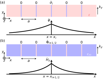
Point and Dipole Fields.
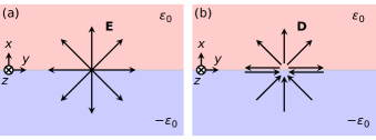
We introduce the fundamental fields with symmetry. Consider a half-space in . We begin with the -symmetrized permittivity, which is defined as follows:
| (10) |
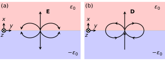
First, we place a point charge at in . The symmetrization is applied to the field in to eliminate the point source. Under symmetrization, the permittivity becomes -symmetric. The obtained field is called a point field and is denoted as with . The most straightforward situation with a uniform is shown in Fig. 1. The second example is the dipole field. Consider a dipole with the dipole moment at in . The symmetrization for the field in removes the dipole source. The obtained field is called a dipole field and is denoted as with . The dipole fields for a uniform are shown in Fig. 2.
Boundary Degree of Freedom.
We show that the degree of freedom of -symmetric fields is represented by either a point field or a dipole field. Consider a half-space electrostatic potential in with . Assuming that there is no free charge in , the boundary charge or dipole may appear at . Let and be symmetric and antisymmetric extensions of in the whole space, respectively. We define and as follows:
| (11) |
| (12) |
These potentials satisfy in with the -symmetrized permittivity defined in Eq. (10). To ensure the boundary condition on for , there should be a boundary charge on satisfying the following equation:
| (13) |
On , the tangential component is continuous, whereas the normal component is discontinuous indicated by . In fact, holds true. A nonuniform may also contribute to the tangential component. Conversely, has discontinuity on , which indicates the existence of a double layer. This is described as follows:
| (14) |
For the double layer on , the normal component is continuous, whereas the tangential component exhibits discontinuity by [18]. Thus, we obtain , which agrees with Eq. (14). Additionally, a nonuniform may contribute to the normal component via electric-field leakage to outside the double layer. From the observation of characteristics of the single and double layers thus far, we can conclude that either or can be used to construct the field in . This statement is consistent with the treatment of a conventional boundary-value problem: the solution to an electrostatic problem is uniquely determined by applying either the Dirichlet or Neumann boundary conditions for each boundary [19]. Now, consider . This field is expressed as follows: in and in ; i.e., the field in is generated from and on in a -symmetrized system. By contrast, vanishes in . To obtain a -symmetric solution, we apply the symmetrization for , which makes both and continuous on . All sources then vanish, whereas the field remains.
Singular Response.
We characterize the singular response of a system. Consider a system with permittivities of in and in . These permittivities do not need to have symmetry. To construct two modes similar to symmetric and antisymmetric modes, we assume the following condition:
| (15) |
which is always satisfactory for a uniform and . Now, we place charges and at and , respectively, with .
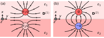
First, consider weighted charges and with , as shown in Fig. 3(a), where the relative permittivity is given as . The electric-displacement field at is given as follows:
| (16) |
satisfies Maxwell’s equations with charge in and . Because holds on , the normal component is continuous on . The electric field fulfills the tangential continuity condition on , owing to the appropriate choice of the charge weights with Eq. (15). Second, we consider and , as shown in Fig. 3(b). The electric displacement is given as follows:
| (17) |
Equation (17) satisfies Maxwell’s equations in and and is antisymmetric with respect to ; therefore, the normal continuity condition of on is satisfied. The corresponding electric field does not have a tangential component on ; hence, the tangential continuity condition on is satisfied.
and represent two solutions for . By combining Eqs. (16) and (17), we can calculate the field for a single charge (e.g., and ). However, results in symmetry, and the weighted charge distribution for becomes exactly the same as that for ; i.e., the charge distribution does not uniquely determine the field. Therefore, leads to the singular response for free charge. When the limit of is taken, and provide the point and dipole fields, respectively. Here, we can exclude the source by removing the slab region and joining and under symmetry.
II.2 Surface Plasmon Polaritons Originating from Symmetry Protection
In this section, we show that surface plasmon polaritons originate from the symmetry-protected electric zero modes. Consider a boundary between the uniform permittivities of in and in . The whole space is assumed to have vacuum permeability . We focus on the transverse-magnetic (TM) surface mode with angular frequency and wavenumber along the direction. The surface impedance on for and is denoted as and , respectively, which are expressed as follows:
| (18) |
The derivation is summarized in Appendices A–C. The resonance condition , which is equivalent to the continuity conditions of the electric field, provides the well-known dispersion relation as follows:
| (19) |
where , , and represent the speed of light in vacuum, vacuum wavenumber, and relative permittivity , respectively.
Equation (19) gives the flat zero band for . The zero modes accompany and at , indicating that only the electric field appears owing to the electromagnetic decoupling at direct current (DC) limit. The origin of the zero modes is the -symmetrized modes shown in Figs. 1 or 2. There are degenerated modes located at different positions on . Because these zero modes do not couple with each other, they form the flat zero band. The eigenfunction with a wavenumber along is obtained by summing point or dipole fields with the weight of the factor like , where we use and the point charge is replaced with the charge density. For , and yield the same eigenmode, because it has both and components. From these observations, we can conclude that the point and dipole fields coalesce. The square-root function in Eq. (19) is multi-valued in the complex plane. This multi-value characteristic indicates that is the exceptional point where the two modes typically coalesce [20]. For , point and dipole fields are decoupled, yielding two modes that produce two waves localized at and .
Now, we can state that -protected zero modes are the origin of surface plasmon polaritons. Starting from , we decrease to . The flat zero band then becomes a finite frequency band. As the deformation induces unbalanced Poynting vectors in and , the energy can propagate with a nonzero group velocity. This -broken mode is usually observed as surface plasmon polaritons in experiments.
II.3 Robustness of Symmetry Protection
The -symmetry protection works for both constant and nonuniform permittivities. Here, we provide two examples to support the robustness of the protection for a nonuniform permittivity configuration.
Layered media.
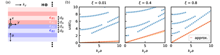
Consider a layered system with metallic and dielectric materials, as shown in Fig. 4(a). The binary dielectric layers are periodically aligned in , whereas the binary metals are periodically arranged with the period in . The thicknesses and of the layers are . In , and with and are assumed. Conversely, we set the relative permittivities in as and , using the parameter . At , the symmetry holds, whereas breaks the symmetry. We focus on nonradiative localized TM surface waves with wavenumber along . Let and be surface impedances at for and , respectively. These impedances can be calculated as the Bloch impedances, as described in Appendix D. The surface-wave resonant condition is represented by . For a given discretized , we numerically evaluate the resonant angular frequency for purely imaginary and .
Figure 4(b) shows real bands of TM surface waves for , , and . The first band (represented by orange circles) distinctly originates from the flat zero modes that are -protected at . As increases from 0, the symmetry is broken, and the first band is raised from zero. The higher bands are sometimes broken because the wave becomes leaky and propagates into infinity. Conversely, the plasmonic first band is nonradiative, and it remains continuous under the perturbation by . This plasmonic dispersion agrees well with the solid red line calculated via the effective-medium approximation, as described in Appendices E and F.
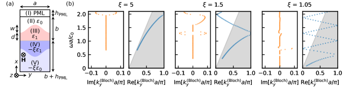
Corrugated system.
Next, we consider nonuniformity in the direction. Figure 5(a) shows the unit cell of a corrugated plasmonic/photonic system with a parameter . The dielectric–metal boundary is located on . The corrugation is periodic in the direction and is given by the function. The geometric parameters are set as , , , and . The permittivity in III is set as . At , the system is -symmetric. We calculated the complex Bloch wavenumber of TM surface waves for a given angular frequency using the conventional finite-element solver COMSOL Multiphysics [21]. To simplify the plot, we restrict satisfying . As the finite-element eigenmode analysis suffers from unphysical modes near the perfectly matched layers (PMLs) [22], we filter the physical modes localized near the surface, using with the complex amplitude of the component of the magnetic field . Here, the complex amplitude is defined as for the real magnetic field , where represents time.
Figure 5(b) presents the calculated complex dispersion relations for , , and . The wavenumber becomes complex above the light line because the diffraction by corrugation leads to energy leakage to infinity. This observation validates the results. At , there is a -protected zero mode at each point on the dielectric–metal boundary . These degenerated modes produce infinite bands in . Therefore, the -protected zero modes are regarded as the sources of infinite bands. When approaches 1, the frequencies of all plasmonic bands decrease to zero. Note that lower eigenfrequencies are missing due to simulation limitation i.e., these modes are weakly confined and affected by the finite simulation domain.
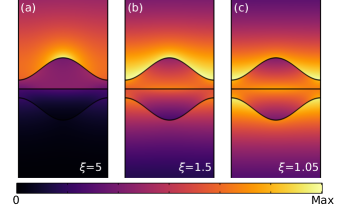
To illustrate the protection more explicitly, we present the electric-field amplitude of the first band at approximately in Fig. 6. When approaches 1, the field becomes symmetric with respect to the dielectric–metal boundary . This result supports the crucial role of symmetry in the formation of surface plasmon polaritons even if the system has nonuniformity.
II.4 Zero-mode Excitation at Temporal Boundary
We showed that surface plasmon polaritons originate from the -protected zero modes. However, realistic configurations break the symmetry; hence, we cannot experimentally observe the surface plasmon polaritons at zero frequency. Now, a question arises: can we observe any zero modes originating from a similar symmetry? We answer this question by constructing magnetic zero modes observable at a temporal boundary.
Assume that the permeability satisfies in . We consider a localized magnetostatic field in . The magnetic field and magnetic flux density in are denoted as and , respectively. Let be the mirror-reflection operation with respect to . The -symmetrized magnetic fields in the entire space are constructed via the concatenation of and . We should carefully consider the axial (twisted) characteristics of magnetic fields when we operate . The symmetrized fields satisfy Maxwell’s equations under the -symmetrized permeability is expressed as follows:
| (20) |
On , the symmetry automatically ensures the continuity condition on . Conversely, tangential magnetic fields ( and ) may not be continuous. To compensate for the discontinuity, we place a perfect metal at that supports surface currents.
This procedure is then applied to a vacuum. A magnetic potential is introduced to produce a magnetic field . Let be a complex constant and consider a magnetic potential with a wavenumber along the -axis. The -symmetrized complex magnetic potential omitting is given as follows:
| (21) |
Then, the surface current on is given as follows:
| (22) |
We emphasize that Eqs. (21)–(22) represent a magnetic zero mode, and the fields are kept unchanged under time evolution. It is important to see that for . Therefore, the magnetic flux perpendicular to the perfect electric conductor on is frozen, which is similar to flux pinning in a superconductor.
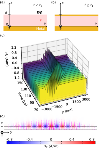
Next, we numerically demonstrate the flux pinning at a temporal boundary. The waveguide is made of a dielectric material with relative permittivity and occupies in vacuum conditions [Fig. 7(a)]. The bottom side () of the dielectric is assumed to be a perfect electric conductor. Such a half-metalized dielectric waveguide possesses surface modes. We focus on the transverse-electric (TE) surface modes (, ) with a wavenumber along the -axis. Consider a lowest-band TE Gaussian wave packet. The wave packet is uniform in the direction and propagates in the direction over time. At time , we metalize the top surface () and maintain it after [Fig. 7(b)]. Therefore, a temporal boundary appears at , resulting in scattering with zero-mode excitation. The source of the zero mode is the surface current on . The zero mode survives even if the mirror symmetry with respect to is broken. The above configuration was realized experimentally for a terahertz wave packet via the photoexcitation of GaAs. Following Ref. 23, we selected and (GaAs). The time-domain dynamics were calculated using COMSOL Multiphysics. Details and justification of the simulation are presented in Appendix G.
Figure 7(c) shows the time evolution of on the top surface on . This top surface is metalized at . At , the wave packet propagates in the direction. For , the wave packet is completely pinned, considering that the metallic boundary does not carry finite-frequency modes with at the boundary. A movie illustrating the temporal dynamics of the two-dimensional is presented in Supplemental Material 111A movie illustrating magnetic-field dynamics near a temporal boundary is provided as an ancillary file in arXiv.. These results indicate the zero-mode excitation at the temporal boundary. The zero mode was expected to be excited in the experiments of Ref. 23, although the zero-mode observation poses a technical challenge. Because the mechanism of flux pinning is universal and independent of the frequency, flux pinning can be experimentally observed at a frequency below the terahertz range for a thick waveguide.
To examine the topological characteristics of the zero modes, we plotted the magnetic-field vector with near at , as shown in Fig. 7(d). Interestingly, the magnetic field rotates as increases. The rotation direction is determined in each and . This feature can be explained as follows: For , a magnetic potential produces a circular rotation in the localized magnetic field. For , there are right- and left-circular components. The boundary condition on determines the weights of these components. Then, right- and left-circular amplitudes equally appear at . Because one of them represents an attenuated solution along , the other component is superior. Therefore, the rotating direction is also determined in . The whole solution is constructed by continuously connecting these solutions at .
Finally, we comment on the analogy between electric and magnetic surface plasmon polaritons. To construct the magnetic analogy to surface plasmon polaritons, we introduce the magnetic conjugation operation for a magnetic field and magnetic flux density . The -protected magnetic plasmon polaritons appear at zero frequency, in addition to the electric ones. Note that the pinning modes excited at the temporal boundary differ from the magnetic surface plasmon polaritons. The pinning modes are originally protected by symmetry rather than the symmetry.
III Topological Polarization Rotation and Surface Impedance
In this section, we examine the general characteristics of the zero-mode field distribution. The zero modes accompany vector-field rotation, as shown in Fig. 7(d). We analyze a similar rotation in electric zero modes and identify Keller–Dykhne self-duality as its physical origin. Lastly, we show that the rotation is directly related to surface impedance, which characterizes the half-space response.
III.1 Uniform Layer
In this subsection, we investigate polarization rotation in a uniform medium with the Keller–Dykhne self-duality between the electric field and electric displacement.
Solutions.
The uniform dielectric (or metallic) slab is an elementary building block for studying surface waves in layered media. Here, we establish the fundamental property of the basic solutions. Consider an electrostatic field in a slab with uniform scalar permittivity located in (). Assume that the wavenumber is given by in the direction, and the electric field is on the plane. The boundary conditions on are regarded as arbitrary. The electrostatic potential is represented by . Using constants and , the two independent solutions are expressed as follows:
| (23) | |||
| (24) |
which represent the waves localized at and , respectively. Note that a variable with a tilde dependent only on represents the complex amplitude omitting in our convention for layered media. The corresponding electric fields are calculated as follows:
| (25) | ||||
| (26) |
These fields involve circular polarizations, although they do not evolve with time because they are electrostatic. Considering the omitted term, the electric field rotates as increases. We stress that the polarization and momentum (or wavenumber) are locked; the wavenumber is flipped when we reverse the polarization rotation. In fact, we can observe and by applying the mirror reflection for Eqs. (25) and (26).
Focusing on the mirror symmetry on , we can construct -symmetric and antisymmetric solutions as follows:
| (27) | ||||
| (28) |
where and are constants. We consider that these symmetric and antisymmetric fields are defined on the circle , which is equivalent to an interval when identifying with . The single- and double-layer charges at (mod ) in give physical sources for Eqs. (27) and (28), respectively. Therefore, the single- and double-layer sources produce the two localized modes at and .
For , special care is required, considering that a constant electric-field potential implies zero electric field. When we maintain () as constant and take the limit of , Eqs. (27) and (28) give the electric fields of and , respectively. Therefore, these constant fields originate from two modes localized at .
The constant electric fields and are directly related to the topology of . At , the equation has symmetry. Therefore, the electric field is decoupled into the and components. The former and latter solutions are -symmetric and -antisymmetric, respectively. We denote the parities (i.e., eigenvalues) with respect to and as and , respectively. The constant electrostatic fields with only exist for . Moreover, the source at (mod ) in vanishes. Therefore, with corresponds to the generator of a de Rham cohomology group of . Upon rotating by radians, we obtain with , which is considered as the unit normal on .
Keller–Dykhne Duality.
The appearance of circular polarization in Eqs. (25) and (26) can be explained by the Keller–Dykhne self-duality.
First, we introduce Keller–Dykhne duality [25, 26, 27, 28]. Let and be a static two-dimensional electric field and an electric displacement, respectively. The Keller–Dykhne duality relates with its dual . We assume that these vector fields only have in-plane components of and and satisfy Maxwell’s equations as follows:
| (29) |
The constitutive relation is expressed as follows:
| (30) |
Consider that the dual fields defined as follows:
| (31) |
where represents the constant permittivity, and is the unit vector along the -axis. The operation induces rotation by radians with respect to the -axis. These fields satisfy Maxwell’s equations, as follows:
| (32) |
The relationship between and is given as follows:
| (33) |
In summary, the Keller–Dykhne duality can relate solutions in different permittivity distributions in Eqs. (30) and (33).
The uniform slab with constant is self-dual when we choose . The solutions can be classified as eigenstates under the rotation . The eigenvectors of are given as circular polarizations with the unit vector along the axes, whereas the corresponding eigenvalues are , respectively. Therefore, Eqs. (25) and (26) involve circular polarizations.
F0 Matrix.
The conventional F matrix is defined for a pair of electric and magnetic fields, as indicated by Eq. (68). However, electric and magnetic fields are decoupled at zero frequency. Thus, we introduce an F0 matrix in the electrostatics, by which electric and electric displacement fields are multiplied. We consider a slab located in with a uniform scalar permittivity . The F0 matrix connects the fields at as follows:
| (34) |
Using the linear combination of Eqs. (25) and (26), is calculated as follows:
| (35) |
Here, holds owing to the reciprocity of the scalar permittivity, as discussed in Appendix H.
III.2 Nonuniform Multilayer
In this subsection, we show that the direction of electrostatic polarization rotation is conserved even in a multilayer dielectric material; hence, it is considered a topological property. Next, we examine the relationship between the polarization rotation and the surface impedance of a half-space.
Multilayer Solution.
We select along . Each region of is occupied by a uniform slab with the scalar permittivity (). The width of each slab is expressed as . The magnetic permeability is for all regions. We assume that the region of has a constant permittivity . If is finite at zero frequency, holds from Eq. (61). As the field should not diverge at , we may set the field at for as follows:
| (36) |
The continuity condition on and allows us to multiply F0 matrices to obtain the solution. In fact, we can calculate the field at satisfying as follows:
| (37) |
where the F0 matrix is denoted as with the parameters and .
Topological Polarization Rotation.
The multilayer solution of Eq. (37) generally includes both left and right circular polarization owing to self-duality breaking caused by the nonuniform permittivity. However, when the signature of is the same for all , the direction of polarization rotation is conserved in .
Consider for all . Assume that has the form of (, ), which is satisfied by Eq. (36). Using the F0 matrix, can be calculated as follows:
| (38) |
has the same form of (, ), because , , , and are positive. Therefore, we deduce that at any point in . The same conservation law can be justified even for a periodic system with infinite layers [e.g., of Fig. 4(a)], as shown in Appendix J.
The electrostatic potential for can also give the solution for the permittivity distribution . Therefore, still holds at any point in for ().
Relationship Between Polarization Rotation and Surface Impedance.
To relate the polarization rotation to the surface property, we consider the case of a finite angular frequency . We define at . From Eq. (61), is related to the surface impedance for as follows:
| (39) |
where represents the permittivity at , and we explicitly express the dependence on , , and in .
As indicated by the previous discussion on the topological polarization rotation, holds. Therefore, all-positive and all-negative permittivity distributions lead to and , which indicate that the half-space is capacitive and inductive at zero frequency, respectively. When is finite at the DC limit, we obtain , which indicates the electric–magnetic decoupling at the DC limit.
IV Bulk–Edge Correspondence to Guarantee Existence of Surface Plasmon Polaritons
In this section, we establish bulk–edge correspondence, which generally ensures the existence of surface plasmon polaritons even with nonuniformity.
In the previous section, it was shown that defines a topological quantity in the half-space. is directly related to the topological polarization rotation of electrostatic fields. and indicate that the half-space exhibits capacitive and inductive behavior, respectively, in the DC limit. Now, we conjecture the bulk–edge correspondence as follows: There always exists a surface mode between two half-spaces with different for a given . First, we examine examples of the bulk–edge correspondence. However, it is difficult to justify the bulk–edge correspondence while focusing on static electric fields alone. To overcome this problem, we consider the magnetic response and frequency dispersion. Then, the bulk–edge correspondence is generally proved with the circuit-theoretical consideration.
IV.1 Empirical Reasoning
In this subsection, we consider examples of the surface-wave formation on the boundary between media to justify the bulk–edge correspondence.
Consider the boundary between a dielectric material and metal, as discussed in Sec. II.2. The dielectric and metal regions with and have and , respectively. Note that the definitions of and are changed to and for . If , Eq. (19) gives a real eigenfrequency. Conversely, the imaginary eigenfrequency appears if is satisfied; however, the modes are still localized at . In both cases, there is a surface plasmon polariton for a given .
Next, we consider a nonuniform scalar permittivity distribution. In , assume that , which is periodic in with a period of . In , satisfies , which is periodic in with a period of . Although it is difficult to prove that the boundary has a surface mode generally, we can analyze its existence in two specific cases: (i) and (ii) for . In (i), the surface wave is tightly localized at . Therefore, the configuration is approximated as the boundary between and , which is reduced to the previous configuration. Therefore, the surface wave exists for a given . In (ii), the surface wave is loosely trapped at ; therefore, we use the effective-medium approximation. In , the effective relative anisotropic permittivities along the and directions are given as and , respectively. Similarly, and are defined for . The surface impedances on are denoted as and for and , respectively. As described in Appendices E and F, the resonance condition of gives the following dispersion relation:
| (40) |
Additionally, we can directly show that the mode with Eq. (40) is bounded on the surface and that the field varies slowly in compared with . Therefore, the surface mode always exists for (). Although the case of a general wavenumber [excluding (i) and (ii)] is difficult to handle rigorously, we can heuristically justify the bulk–edge correspondence as follows. Consider () and (). The magnetic permeability is given by the vacuum permeability . Next, we continuously deform in so that symmetry is satisfied, while keeping constant. Then, the symmetry ensures the existence of the surface zero modes. Under the deformation, the eigenfrequency can continuously change; that is, a new mode is not created, an existing mode is not annihilated, and a localized state does not suddenly change to a diverged one and vice versa. We follow the above process in reverse. Then, the surface mode exists in the original configuration as long as its frequency is kept low to avoid energy leakage to infinity. However, the above reasoning has not been validated.
IV.2 Bulk–Edge Correspondence from Circuit-Theoretical Consideration
To overcome the challenge for proving the bulk–edge correspondence, we introduce circuit-theoretical concepts and use them to prove the bulk–edge correspondence.
Classification of Response at Zero Frequency.
The passive driving impedance must be a positive-real function of , where represents the angular frequency [29]. If the circuit is lossless, is an odd function owing to the time-reversal symmetry. Then, a physically possible lossless impedance is an odd positive-real function that satisfies or [30]. We can infer that these responses originate from electric and magnetic zero modes, as discussed in Sec. V.3. The reactance theorem ensures that increases monotonically as increases. Therefore, indicates that behaves inductively near . By contrast, suggests a capacitive response near with . In summary, the frequency response is classified as when there is a gap near zero frequency. The above properties are valid even for a continuous (distributed-element) model because the system can be modeled by finite numbers of inductors and capacitors when we set the spatial discretization small enough for the typical length scale of the focusing phenomena.
The above properties can be confirmed in simple examples. The first example is a vacuum. From Eq. (18), the TM vacuum surface impedance is given as follows:
| (41) |
Clearly, holds, and the vacuum is capacitive near zero frequency. The second example is metal, which can be modelized using the following Drude permittivity [31]:
| (42) |
where represents the plasma angular frequency. Accordingly, the TM surface impedance of metal is expressed as follows:
| (43) |
For , can be approximated as follows: , where represents the vacuum impedance. Then, the metallic half-space behaves as an inductor. We stress that an electric field does not exist (i.e., ), because diverges at zero frequency. From under , only a magnetic field () can exist.
General Properties of Surface Impedances.
Consider a dispersive metal with and located in . For example, we assume
| (44) |
with background permittivity and plasma angular frequency . Inside the Drude metal, electric fields vanish at . In fact, Eq. (61) is approximated as near . Therefore, holds true and is possible at . Similarly, is deduced from Eq. (62) under the assumption of a finite . Then, is expected as the TM metal response.
In , we consider a distributed with . Assume that satisfies and (). The first assumption is reasonable because usually accompanies strong frequency dispersion. Additionally, the second assumption is justified, because finite region is enough to be considered for localized waves. Let be the surface impedance of the half-space . At , holds from the discussion of topological polarization rotation.
Now, we prove that includes a zero in . This lemma is used in the proof of the bulk–edge correspondence. We begin with a uniform vacuum. The surface impedance of Eq. (41) is purely imaginary, and has zero at . We prove that the zero is kept in even when we gradually insert dielectric slabs in . First, we consider adding a dielectric slab with thickness and permittivity (). This slab is placed in . Second, the whole system is translated by along so that the surface is located on . After the insertion and translation, is still purely imaginary for . At , the wavenumber along and impedance inside the added dielectric should satisfy and , respectively. If there is a zero at in the initial , the insertion and translation lead to as observed from Eq. (69). Considering a small , we determine . Therefore, the zero at always goes to the lower frequency after the gradual insertion and translation. The insertion is repeated until is obtained. From the above discussion, the gradual insertion of the dielectric keeps the zero inside .
Proof.
Now, we complete the proof of the bulk–edge correspondence. The lowest angular frequency satisfying inside is denoted as . First, we consider the case of . The following three conditions are satisfied: (i) is purely imaginary in , and monotonically increases with ; (ii) ; and (iii) . Under these conditions, the intermediate value theorem ensures that there is an angular frequency at which is satisfied. There may be poles of , and the intermediate value theorem should be extended to handle infinity. Even if unexpectedly holds, we can introduce as the lowest angular frequency in , satisfying at . Then, we can apply a similar discussion for to ensure the existence of a zero in . Thus, there always exists a surface localized mode at the boundary between media, under the physical assumption.
IV.3 Relationship Between Symmetry Protection and Bulk–Edge Correspondence
Finally, we discuss the relationship between the -protected zero modes and the bulk–edge correspondence according to physical constraints. Although their theoretical foundations differ significantly, they are related to each other. We examine the relationship while focusing on a conventional surface-plasmon polariton. Assuming that is filled with a dielectric material with constant permittivity whereas is occupied by a metal with the Drude response [Eq. (42)], our bulk–edge correspondence ensures the existence of a surface wave with the dispersion relation . For a given , we define a frequency-independent permittivity . Now, consider the boundary between and . It gives the original surface plasmon polariton only at . When we gradually transform into , the surface mode at becomes the -symmetric zero mode. Thus, the bulk–edge correspondence predicts a mode originating from a -protected zero mode.
V Essential Understanding of Dielectric–Metal Transition Based on Minimal Circuit Model
In Sec. IV, we established the bulk–edge correspondence, which generally explains the existence of surface plasmon polaritons between a metal and a dielectric material even with nonuniformity. Now, a question arises: how can we understand the essential difference between metals and dielectrics from the perspective of the band theory? Although we can attempt to solve this problem directly using a continuous model, its complexity blurs the underlying physics. Therefore, we take a different approach. We propose and analyze a minimal circuit model, which induces a topological transition. Furthermore, we show that the minimal model can accurately explain the dielectric–metal transition. Finally, the transition is understood as the interchange between electric and magnetic zero modes. Our approach highlights essential physics in the topological transition without distractions.
V.1 Composite Right/Left-Handed (CRLH) Transmission Line
The CRLH transmission line was historically introduced to investigate the negative refractive index from a circuit-theoretical perspective [4]. Herein, we show that the CRLH transmission line is considered a minimal model for inducing a topological transition with duality.
Model.
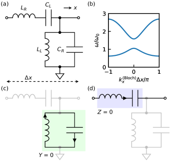
Figure 8(a) shows the unit cell of a CRLH transmission line with inductors and capacitors. The unit cell is periodically arranged in the direction with period . When the left-handed parameters are set as and , the model becomes a conventional transmission line. The right-handed components are characterized by and . For the left-handed components, we introduce dimensionless parameters and . The dispersion relation of a CRLH transmission line for and is depicted in Fig. 8(b) (see Appendix K for calculation details). Here, and represent the Bloch wavenumber along and the angular frequency, respectively. The left-handed components and produce the remarkable first band with a negative group velocity, whereas the second band corresponds to the first band for the conventional transmission line with and . From the perspective of electromagnetism, the negative group velocity indicates a left-handed triad of an electric field, magnetic field, and wave vector, whereas the conventional transmission line has a right-handed one. The name “CRLH transmission line” originates from the fact that it contains both right- and left-handed elements.
Series and Shunt Resonances.
The CRLH transmission line has mirror symmetry when the order of the inductor and capacitor positions in the series impedance and the shunt admittance are ignored 222 In particular, a CRLH transmission line has mirror symmetry with respect to or , as described in the effective model of Fig. 14.. Because the mirror symmetry still holds at the band edge of the wavenumber space, the band-edge eigenmodes are classified as symmetric and antisymmetric modes. We focus on eigenmodes with . Thus, a symmetric mode must not accompany a series current, whereas an antisymmetric one leads to a node voltage of zero. Therefore, the symmetry demands the resonance conditions ( or ). The corresponding resonant modes are depicted in Figs. 8(c) and (d), and their angular eigenfrequencies are expressed as follows: and , respectively. Clearly, the node potential in Fig. 8(c) is symmetric and the series current in Fig. 8(d) is antisymmetric with respect to the mirror reflection. The band gap appears between and .
Topological Phases.
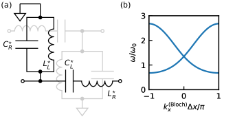
CRLH transmission lines can be classified into two topological phases: (i) and (ii) . When we gradually change the parameter from (i) to (ii), band inversion occurs at . This transition induces the flipping of the eigenmode parity at . Therefore, the parity is a topological integer characterizing the transition.
Duality.
The two topological phases are implicitly related through the circuit duality. Consider a dual circuit for the CRLH transmission line with respect to a reference resistance , as shown in Fig. 9(a). We obtain the dual quantities as follows:
| (45) | ||||
| (46) |
Equation (45) becomes self-dual, i.e., and , provided that we set as follows:
| (47) |
Under duality transformation, the left-handed component is transformed into
| (48) |
Therefore, the duality transformation induces the interchange between and . In particular, the swap maintains the shape of the dispersion relation, whereas the symmetry of eigenmodes is interchanged at . The self-duality characterizes the transition point of the two phases as . Figure 9(b) shows the dispersion curve for . We can clearly observe the Dirac-point formation at , which is protected by self-duality.
Bulk–Reactance Correspondence.
Each topological phase has a definite sign of the Bloch reactance inside the band gap. We prove this bulk–reactance correspondence from a circuit-theoretical perspective. The symmetries of the eigenmodes demand and , as shown in Figs. 8(c) and (d), respectively. The band gap is denoted by with and . In , is purely imaginary, and has no zeros or poles. Because monotonically increases with an increase in from the reactance theorem, the band-gap behavior in is determined as follows: (i) capacitive response for or (ii) inductive response for . Therefore, we have completed the proof. As shown in Appendix L, the definite sign of the Bloch reactance inside a band gap can be established even in a continuous (distributed-circuit) model.
Note that the parity at is kept unchanged under the transition between the two phases of (i) and (ii). Thus, it does not affect the surface impedance inside the band gap. The parity at depends on the choice of the unit cell. In fact, and T units give different parities at (see Appendix K). Therefore, the conventional formula involving the Zak phase [33] cannot be naively applied to plasmonic systems.
V.2 CRLH Model for Dielectric–Metal Transition
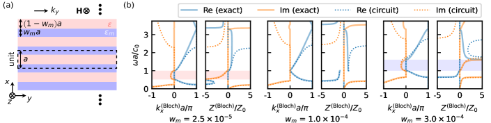
We show that the CRLH transmission line reflects underlying physics of the topological dielectric–metal transition. Consider dielectric and metallic layers, as indicated by the dashed box in Fig. 10(a). The bottom of the unit cell is selected as the center of the metal to simplify the Bloch impedance. We analyze a TM wave with wavenumber in the direction. The period of the unit cell in the direction is denoted as . The dielectric layer has thickness and permittivity . The speed of light in the dielectric layer is given as follows: . The permittivity of the metallic layer with thickness is given by the Drude model with Eq. (42). By changing the metal portion , we can induce a topological phase transition [13]. To derive a CRLH model theoretically, we focus on , in contrast to Ref. 13. To induce band inversion in , is required.
The TM mode propagation along in the dielectric and metal can be modeled using one-dimensional circuits, as described in Appendices M and N. In developing the circuit model of the binary unit cell, we assume that the positions of the shunt admittance and series impedance can be exchanged freely in the unit cell. As shown in Appendix O, this assumption is justified when the shunt current is sufficiently small compared with the series current. Then, we obtain a CRLH model for the unit cell as shown in Fig. 10(a). The circuit parameters are given as follows:
| (49) | ||||
| (50) | ||||
| (51) | ||||
| (52) |
Next, we analyze the continuous and simplified CRLH models and compare their results. First, we describe our calculation setup. We select and set and . For a given frequency, the Bloch wavenumber along is calculated. The Bloch impedance in the exact model is evaluated at the bottom of the unit cell (i.e., the center of the metal). The continuous model is treated as described in Appendix D, whereas the circuit model is analyzed based on Appendix K. The circuit model exhibits ambiguity in defining . It is calculated for the unit so that is inductive near (see Appendix K). In both systems, we select the solution that does not diverge at . Then, the following condition is imposed:
| (53) |
To simplify the plots, we only include the modes obeying the following condition:
| (54) |
Because the CRLH transmission line has time-reversal symmetry, we can produce solutions satisfying by applying the time-reversal operation to the solutions satisfying Eq. (54). The symmetry consideration indicates the following properties: (i) the Bloch wavenumber and impedance are real or purely imaginary and (ii) the Bloch impedance must be 0 or at the band edge , as described in Appendix L. Because and can be imaginary, we plot their real and imaginary parts with respect to the frequency.
Figure 10(b) shows the Bloch wavenumber and impedance evaluated using the two methods. The circuit model solution (dotted) agrees well with the exact solution (solid) below the bottom part of the second real band. Therefore, the circuit model substantially captured the band inversion between the first and second bands. We stress that the circuit model does not involve any fitting parameters. At the high frequencies, the circuit model does not approximate the exact solution well. This disagreement is reasonable considering that the circuit model involves only a few degrees of freedom, whereas the exact model has an infinite degree of freedom. In fact, the exact treatment produces an infinite number of bands, whereas the circuit model only yields two bands. The shunt–series swapping to obtain the CRLH model is justified as follows. In the circuit model, the series impedances of the dielectric and metallic regions are represented by and , respectively, and the shunt admittances are represented by and , respectively. Because we focus on , becomes small. Then, becomes large except for at which exhibits the resonance. Therefore, is expected at . At , becomes zero, and holds. In conclusion, both cases satisfy the swapping condition presented in Appendix O.
We explain the transition in terms of the CRLH model. Using Eqs. (49)–(52) with , the CRLH parameters are determined as follows:
| (55) | ||||
| (56) | ||||
| (57) | ||||
| (58) |
Therefore, () holds for small , whereas () holds for large . Figure 10(b) presents the crossover between them. The mirror symmetry leads to at , whereas the antisymmetry results in at . If is satisfied, is required for the reactance theorem. Hence, the gap behaves capacitively; for . By contrast, demands ; thus, the gap behaves inductively: for . These bulk–reactance correspondences are confirmed for the filled regions in Fig. 10(b).
Now, we consider and . The dielectric limit gives , resulting in and , which is the cutoff frequency of the dielectric material. The metallic limit leads to , resulting in and . Therefore, the plasmonic gap forms in . We need not consider the approximation condition of at , because the additional capacitor ( discussed in Appendix N) does not contribute to the resonance frequencies. Shunt and series zero modes with different symmetries at and are responsible for the frequency responses in the quasistatic regime, which are given by and , respectively.
Now, we clarify the difference between the bulk–edge correspondence established in Sec. IV and the bulk–reactance correspondence proven here. The bulk–reactance correspondence indicates capacitive and inductive behaviors for for and , respectively. Therefore, it is implicitly related to an LC resonance; however, it does not generally ensure the existence of such a resonance. The existence of surface plasmon polaritons on metals is explained by the previous bulk–edge correspondence.
V.3 Electric and Magnetic Zero Modes
In this subsection, we identify localized zero modes, which produce the flat zero bands at the dielectric and metallic limits. They are responsible for the zero resonances discussed in Sec. IV.2 and give the physical origin of the extraordinary first band with a negative group velocity.
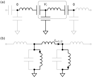
From the perspective of the circuit model, responses at and originate from the zero modes shown in Fig. 11. These zero modes are bulkily degenerated and form flat zero bands. They are dual with each other and have constraints on the total charge in a cut set comprising capacitors or the flux penetrating a loop comprising inductors. These constraints can be interpreted as DC freezing, under the limit of or . Next, we construct the corresponding states in the continuous model.
First, we investigate . We consider the F0 matrix of a single metallic layer at with an infinitely thin thickness . From Eq. (35) with for , the continuity is deduced as . Conversely, may have discontinuity at , which represents the charge degree of freedom at the layer. Although the charge cannot exist for , insertion of an infinitely thin metallic layer at adds the degree of freedom. The infinitely thin layer works only for and does not contribute to the frequency response for , considering that the permittivity is finite at . Therefore, the insertion is interpreted as a zero-mode addition. For a periodic system with , we can construct a zero mode generated by a charge located only on a single layer by using the solution of Eq. (23). The constructed mode is shown in Fig. 12(a) and corresponds to Fig. 11(a). The zero modes compose the flat zero band considering that they form at all layers.
Second, we analyze . We start with . From Eqs. (61)–(63), the inside the Drude metal obeys
| (59) |
which is reduced to for . Therefore, the zero-frequency solutions are given by . By contrast, electric fields inside the metal approach zero for from Eqs. (61) and (62). Now, we place a single gap at inside the Drude metal. It has an infinitely thin thickness and permittivity . From Eq. (69), we conclude that is continuous at for . However, may possess a discontinuity at , which indicates a discontinuous at from Eq. (62). The discontinuity is interpreted as the magnetic-flux degree of freedom. Therefore, the insertion of an infinitely thin dielectric slab into a metal involves a zero-mode addition, whereas the frequency response is kept unchanged for . Finally, we can construct a magnetic zero mode, as shown in Fig. 12(b), corresponding to Fig. 11(b). Each layer has an individual zero mode, resulting in the flat zero band.
In summary, electric and magnetic zero modes exist at and and are responsible for the zero resonances discussed in Sec. IV.2. They highlight the essential difference between dielectrics and metals. The change in from to induces the interchange between the electric and magnetic zero modes, resulting in the phase transition.
VI Conclusions
In this study, we revealed the origin of surface Maxwell waves. The results indicated that the surface plasmon polaritons originate from robust electric zero modes with symmetry. The similar zero modes can be experimentally excited at a temporal boundary. Owing to the Keller–Dykhne self-duality, the zero modes possess real-space polarization rotation, which is related to the surface impedance. Furthermore, the bulk–edge correspondence can be summarized as follows: a surface mode exists between the inductive and capacitive surfaces. However, this statement cannot be proved when focusing on electric zero modes alone. To solve this problem, we introduced magnetic response and frequency dispersion. Then, we generally proved the bulk–edge correspondence with circuit-theoretical considerations. Finally, we proposed a CRLH transmission line with duality, fully explaining the essential physics underlying the topological transition between a metal and a dielectric material. In summary, surface plasmon polaritons are comprehensively understood from two different viewpoints: symmetry protection and bulk–edge correspondence, which are related to each other. The elucidated physics of surface Maxwell waves is now within the reach of experimental verification.
Acknowledgements.
The authors thank A. Okamoto, J. Matsudaira, Y. Shikano, H. Maruhashi, and A. Sanada for their fruitful discussions. This work was supported by JST, PRESTO (Grant No. JPMJPR20L6), and JSPS KAKENHI (Grant Nos. 19K05304, 20K14374, 20H01845, 22K04964, and 22H00108).Appendix A Basic Equations of Surface Plasmon Polaritons
Assume that the electric permittivity and magnetic permeability depend on alone. Consider a TM wave with wavenumber in the direction. It has a -component magnetic field with the complex amplitude . Similarly, we define the complex amplitudes of the electric displacement , electric field , and magnetic flux density . Here, we use the convention that a variable with a tilde dependent only on always represents the complex amplitude omitting . The laws of Gauss, Ampére–Maxwell, and Faraday are given by the following equations:
| (60) | ||||
| (61) | ||||
| (62) | ||||
| (63) |
Note that these equations are not independent. Eq. (61) and Eq. (62) lead to Eq. (60) for , although Eq. (60) should be independently demanded at .
Appendix B F Matrix of Slab for TM Waves
A uniform slab is located in () with the real scalar permittivity and permeability . We derive the relationship between the fields at and . Consider a TM wave, where the magnetic field is oriented in the direction. The angular frequency and wavenumber along the -axis are represented by and , respectively. The complex amplitude of the component of the magnetic field is represented as
| (64) |
where we omit the temporal variation and spatial variation . The wavenumber satisfies
| (65) |
Using the Ampére–Maxwell equation, we obtain the component of the electric-field amplitude as
| (66) |
where we define the TM wave impedance as
| (67) |
From Eqs. (64) and (66), the fields at and are related as follows:
| (68) |
The F matrix of the slab with thickness is given as
| (69) |
where is the propagation constant. There are two sign choices for in Eq. (65); however, both give the same F matrix. Conventionally, is defined so that the term represents the physical mode in a half-space, as discussed in Appendix C. Equation (69) satisfies
| (70) |
which is related to the reciprocity [34].
Appendix C Effective Response of Uniform Half-Space
We characterize the effective response on for a uniform half-space with real scalar permittivity and permeability located in . We use the convention that the terms become physical in the half-space. We separately consider two cases: a real and a purely imaginary . For a real , there are two propagating modes in the direction. One carries energy from to infinity, whereas the other brings energy from to . When we treat the effective response on for the half-space, the latter should be ignored. Therefore, is needed to ensure that represents the energy flow from to . Next, we treat the case of the imaginary . When the terms should be finite at , is required. In summary, the wavenumber along the -axis is defined as follows:
| (71) |
According to Eq. (71), the effective response of the half-space is represented by , which is defined in Eq. (67).
Appendix D Bloch Analysis of Periodic Binary Dielectrics
With regard to Secs. II.3 and V.2, we consider a periodic arrangement of binary slabs composed of and . Let and be two dielectric materials with permittivities and , respectively. The unit cell of thickness is filled with and in and , respectively. We periodically arrange the unit cell in . The wavenumber in is denoted as . We define and . The unit F matrix obtained from the multiplication is given as
| (72) |
Here, we introduce the wave impedance as
| (73) |
The Bloch wavenumber is given as
| (74) |
When we focus on the decaying wave in the positive direction,
| (75) |
is required. Using , we obtain
| (76) |
Here, the trace can be calculated as
| (77) |
The Bloch impedance on for is given as
| (78) |
Appendix E Effective-Medium Approximation of Periodic Layers
For Secs. II.3 and IV.1, we introduce the effective-medium approximation for periodic layers. We choose , , and satisfying . The uniform slabs with permittivity occupy the region of (). The slab width is denoted as . A unit cell with thickness consists these slabs. The unit cells are periodically arranged in . If the typical length of spatial field variation is significantly longer than , the system behaves as an anisotropic medium with permittivities and along the and -directions, respectively.
First, we derive the effective parameter . We apply an electric displacement along . From the boundary condition, is constant along . Considering with , we obtain
| (79) |
Thus, we must average to calculate .
Second, we determine the effective parameter when applying an electric field in . The -component electric field is constant along owing to the boundary conditions. From with , we obtain
| (80) |
which indicates that the average of gives .
Appendix F Surface Plasmon Polaritons on Anisotropic Medium
For Secs. II.3 and IV.1, we derive the dispersion relation of surface plasmon polaritons between anisotropic media with diagonalized permittivity tensor components along , , and . The permeability is assumed to be in the entire space. In , we consider a dielectric material with the permittivity-tensor components and along the - and -axes, respectively. In , we place a metallic material with the permittivity-tensor components and along the - and -axes, respectively. We focus on a TM wave with wavenumber along . From Eqs. (61)–(63), we obtain
| (81) |
where we use the relative permittivity . When we assume () and (), the decay constant can be calculated as
| (82) |
Let and be the surface impedances on for and , respectively. The surface impedance can be calculated as
| (83) |
The resonance condition is reduced to
| (84) |
Because and are satisfied, can be positive. From Eqs. (82) and (84), we obtain
| (85) |
From Eqs. (82) and (85), it is possible to confirm that , which indicates that the mode is localized at the boundary.
Appendix G Simulation Details on Temporal Boundary
For Sec. II.4, we explain the details of the simulation of the temporal boundary. We focus on the sudden temporal shift from a single-metalized waveguide to a double-metalized waveguide, as shown in Figs. 7(a) and (b). The temporal transition of the boundary resistance causes a dispersion change in the waveguide. Owing to the spacetime continuity condition, the wave vector must be conserved at the temporal boundary. The incident field in the single-metalized waveguide is redistributed to a series of different frequency modes in the double-metalized waveguide. This process is decomposed into scattering from the incident wave to the th mode. The mode number of the double-metalized waveguide is denoted as , in order from the lowest frequency of the zero mode (). The mode with has the transverse wavenumber in . The temporal dynamics were simulated using the transient analysis (temw) module in COMSOL Multiphysics.
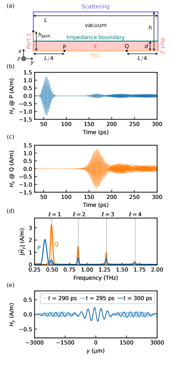
The simulation setup is shown in Fig. 13(a). A dielectric slab made of GaAs with is placed in under vacuum conditions. The geometric parameters are set as , , and . The perfect electric conductor (PEC) boundary condition is imposed at the bottom of the slab (). The top side of the slab () is represented by the impedance boundary with a sheet admittance . is initially set to 0 and is suddenly increased to for . The wave packet is generated from Port 1 located in with . The incident sheet current along in Port 1 is given for as follows:
| (86) |
The incident magnetic field is multiplied by the factor of 2 considering that the incident current is equally divided between the output port resistance and the load, which are connected in parallel, under the matching condition. We choose , , , and , whereas and are semi-analytically evaluated (see Supplemental Material in Ref. 23). The sheet impedance of the port inside the slab is set as that of the double-metalized waveguide, which suppresses the port reflection for the first-order mode. Note that the boundary cannot absorb the other frequency modes. For the outside region, we simply use the vacuum impedance . In summary, the sheet impedance of the port is set as
| (87) |
Although is not correct for the single-metalized waveguide, it works practically. Here, is calculated from the dispersion of the single-metalized waveguide for the given . The angular frequency of the mode in the double-metalized waveguide is evaluated for the calculated . Additionally, we place Port 2 at . No current is excited at Port 2, and its impedance is set as that of the double-metalized waveguide, which is given by Eq. (87). The remaining boundaries are treated as the scattering boundaries. We monitor the magnetic fields at and , which are denoted as P and Q, respectively.
Figure 13(b) shows the temporal variation of at P. We can observe the incident wave packet at approximately and the reflected signals after . The first reflected signal at approximately represents reflection into the mode. By dividing the envelope amplitude of the first reflected by that of the incident one, the absolute value of the amplitude reflection coefficient is estimated as , which agrees well with the theoretical value of . Because the higher-order modes propagate with lower group velocities, they are observed later. In fact, the oscillation frequency becomes significantly higher after . The transmitted signal observed at Q is shown in Fig. 13(c). Similar behavior is observed for the reflected one. The amplitude transmission coefficient of the mode is estimated as , which agrees with the theoretical value of . To analyze the frequency shift, the signals in Figs. 13(b) and (c) are Fourier-transformed with the normalized convention of unitary transformation. The Fourier amplitude is shown in Fig. 13(d). The peak frequencies agree well with the theoretically obtained frequencies of the converted waves, as indicated by vertical dashed gray lines. To investigate the spatial distribution of the zero mode, we plotted along at , and , as shown in Fig. 13(e). The central signal at approximately is steady and represents the zero mode, although the other region exhibits time evolution. The envelope amplitude of the zero mode is divided by the incident one, and we obtain the scattering coefficient of to the zero mode. This value is identical to the theoretical value of . The results validate the simulation.
Appendix H Reciprocity in Electrostatics
In this section, we summarize reciprocity in electrostatics, as discussed in Sec. III.1. Consider two electrostatic potentials and for a reciprocal permittivity (represented by a scalar or a symmetric matrix). The corresponding electric displacements are denoted as and , respectively. When we assume that there is no free charge, the following reciprocal theorem for a three-dimensional region holds:
| (88) |
We apply the reciprocity theorem for a slab presented in Sec. III.1. Consider and assume . For , the complex amplitude of the electrostatic potential is proportional to . When the values are given, the electric displacements are linearly determined as follows:
| (89) |
Let be the complex amplitude of the electrostatic potential for and . Similarly, is defined for and . By applying Eq. (88) for and , we obtain . Finally, is obtained, by transforming Eq. (89) into the form of Eq. (34).
Appendix I Formal Solution for Layered Medium
For Sec. III.2, we construct a formal solution of an electrostatic field. Consider in . From Eqs. (60) and (63) with zero frequency, the following equation determines the spatial variation of the field:
| (90) |
Equation (90) is analogous to Schrödinger’s equation with a time-dependent Hamiltonian. When we assume for , the solution may satisfy
| (91) |
Let be a 2 matrix defined at . The spatially ordering operator acts as follows:
| (92) |
with a permutation that satisfies . Using , we can formally express the field at any point () as follows:
| (93) |
Appendix J Topological Polarization Rotation in Periodic Layered Media
For Sec. III.2, we provide proof of topological polarization rotation in periodic media with infinite numbers of layers. We select and place a dielectric material with (relative permittivity: ) in . We regard as a unit cell and arrange it periodically in with period . Let us consider a TM wave with wavenumber in . First, we show that is purely imaginary at . The F0 matrix of the unit cell has the following form:
| (94) |
The above statement is proved as follows: For , Eq. (35) fulfills Eq. (94). If we multiply Eq. (94) by the matrix in Eq. (35), the obtained matrix also satisfies Eq. (94). Therefore, the statement is proven. From Eq. (94), the eigenvalue of is calculated as follows:
| (95) |
Therefore, must be real. Furthermore, becomes purely imaginary as follows:
| (96) |
Now, we consider an electrostatic field in and assume that (, ). We define and calculate the field at as follows:
| (97) |
This field has the form of (, . Moreover, Eq. (97) indicates that . Repeating the discussion, we can express the field in the form of (, ) at any point. Moreover, does not converge at . Therefore, it does not give a solution. In conclusion, the field can be expressed in the form of (, at any point of , where we used a degree of freedom of the overall scalar factor.
Appendix K Analysis of Ladder Circuits

For Sec. V, we consider a one-dimensional circuit, as shown in Fig. 14. The -axis is discretized with , and the shunt admittance and series impedance are located at and (), respectively. The complex amplitudes of the current flowing through and those of the voltage along satisfy the following equations:
| (98) | ||||
| (99) |
For a periodic system, we assume that and are independent of and denote them as and , respectively. With the Bloch wavenumber , Bloch’s theorem indicates that
| (100) | ||||
| (101) |
By substituting Eqs. (100) and (101) into Eqs. (98) and (99), we obtain
| (102) |
For , Eq. (102) is reduced to , which indicates the existence of symmetric () and antisymmetric () modes. Equation (102) is often used to calculate a dispersion relation for a given . Instead of Eq. (102), we can also determine as
| (103) |
Equation (103) is utilized to obtain a dispersion relation for a given .

We can intuitively understand the eigenmode symmetry at the highly symmetric points in the Brillouin zone. As shown in Fig. 15, we define node potentials and mesh currents , which represent the full degree of freedom restricted by Kirchhoff’s laws [35, 36, 28]. Additionally, we introduce two mirror reflections and on and , respectively. First, we analyze the case, in which and are independent of . Clearly, the constant node potential represents a symmetric degree of freedom (for both and ), whereas the constant mesh current represents an antisymmetric one. Therefore, symmetric and antisymmetric modes can appear at . Next, we examine the case. Here, and are constants regardless of . Interestingly, both degrees of freedom produce the -symmetric (-antisymmetric) distributions. Therefore, the modes at have identical parity.

The Bloch impedance is the effective impedance of infinite circuits seen from left to right. It depends on the choice of a unit cell. Here, we consider two configurations of unit cells, as shown in Fig. 16. For the unit, we can evaluate the Bloch impedance as
| (104) |
It is also calculated for the T unit as
| (105) |
The circuit duality connects these impedances as follows:
| (106) |
Note that and can have different signs when we assume that is real.
Finally, we consider a CRLH transmission line, as shown in Fig. 8(a). The series impedance is expressed as
| (107) |
and the shunt admittance is given as
| (108) |
It is not essential to distinguish which capacitor or inductor is on the left side in , considering that the effective response is unaffected by the interchange of the geometrical positions. We define parameters , , , and . Then, and are expressed as
| (109) | ||||
| (110) |
From Eq. (102), the dispersion relation can be calculated as follows:
| (111) |
Using Eq. (103), we can calculate the complex dispersion relation.
Appendix L Symmetry Constraints
For Sec. V, we summarize the symmetry constraints on the wavenumber and Bloch impedance. Consider TM wave propagation in a layered photonic or plasmonic crystal periodic in with period . One example is the model examined in Appendix D. Here, we derive the symmetry constraints on the Bloch wavenumber and impedance. The same constraints also work in circuits. The assumption of the TM mode is introduced to simplify the explanation and is not essential.
Time-Reversal Symmetry and Reciprocity.
First, we discuss the time-reversal operation. For an electric field , gives the time-reversal phasor of . The phasor of a magnetic field is transformed into . Therefore, the time-reversal operation for is represented by , where is the complex-conjugate operator and . If the system has time-reversal symmetry, and give the solution to the problem.
A real and make in Eq. (69) invariant under the time-reversal operation. Let us examine Eq. (74). The two eigenvalues of are denoted as and . From , according to the reciprocity, and depend on each other as . For , the time-reversal symmetry demands (i) , or (ii) . From these constraints, the distribution of is classified in Fig. 17, where gives the crossover points between propagating and decaying (in-gap) solutions. The time-reversal operation does not change the eigenvalue of the decaying solutions. Therefore, we obtain , which indicates that the Bloch impedance inside a band gap is purely imaginary.

Mirror Symmetry.
Next, we consider a mirror-symmetric unit cell with time-reversal symmetry and reciprocity. Figure 10(a) shows an example. On the mirror-symmetric plane, there are constraints on the Bloch impedance.
First, consider a propagating mode with angular frequency and a real . The invariance under a combination of the mirror reflection and time-reversal operations leads to . Note that the mirror reflection induces the transformation , whereas the time-reversal operation induces . Therefore, the Bloch impedance is real in propagating bands.
Second, we show that or on a mirror plane for and . Here, the period in is denoted as . Because and are invariant under the mirror reflection, the eigenmodes must be symmetric or antisymmetric with respect to the mirror reflection. Owing to the field continuity, the symmetric and antisymmetric solutions must satisfy and on the mirror plane, which results in and , respectively [33].
Third, the reverse of the second statement holds: and at a propagating band indicate symmetric and antisymmetric modes, respectively. We prove this statement for . The -axis is selected such that the unit cell has the mirror planes located on and . The eigenvector of the F matrix can be selected as , which has time-reversal symmetry. Therefore, the wavenumber is restricted to a time-reversal wavenumber of ; i.e., the field is symmetric or antisymmetric on the unit boundary . Therefore, all fields inside the unit cell must be symmetric or antisymmetric. A similar discussion holds for .
Finally, we establish a definite Bloch-reactance sign in a band gap. The band gap is denoted as . The Bloch impedance must be real in a propagating band, whereas it is purely imaginary in a band gap. Therefore, must be or for , which indicates the existence of symmetric or antisymmetric modes. We can safely assume that there is no zero or pole of in . Even if there was a zero or pole in , we would divide the band gap into several segments, each of which fulfills the assumption. Therefore, the reactance theorem maintain the definite reactance sign in each band gap.
Appendix M Analogy Between Circuits and Electromagnetic Systems
For Sec. V.2, we present an analogy between electric circuits and electromagnetic systems. We consider TM-wave propagation along with . The electric field is parallel to the -axis, and the magnetic field is in the direction. These complex amplitudes are denoted as and . The electric permittivity and magnetic permeability are represented by and , respectively. Ampère–Maxwell’s and Faraday’s laws give the following equations with angular frequency :
| (112) | ||||
| (113) |
Clearly, Eqs. (112) and (113) are analogous to Eqs. (98) and (99), respectively. The variable correspondence between the two systems is summarized in Tab. 1.
| Circuit | ||||
|---|---|---|---|---|
| Maxwell |
Appendix N Circuit Models of Dielectric and Metal
For Sec. V.2, we construct circuit models of the dielectric and metal to reproduce their wavenumber () and wave impedance ().
Effective Parameters for TM Propagation.
For the TM wave with considered in Appendix A, we can construct a one-dimensional model along . The effective permittivity and permeability in the one-dimensional model are denoted as and , respectively. From Eq. (67), we obtain
| (114) |
Considering in Eq. (65), should satisfy
| (115) |
Thus, can be obtained as
| (116) |
Circuit Model of Dielectric.
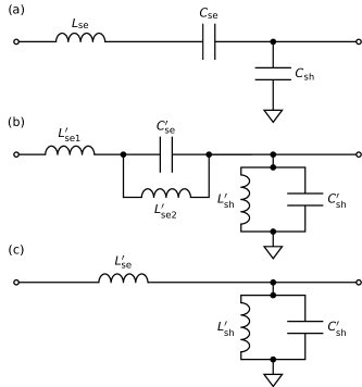
We characterize a dielectric slab with permittivity and vacuum permeability . Eqs. (67) and (71) give the impedance and wavenumber, respectively. Using Eq. (114) and (116), we can extract the effective parameters as follows:
| (117) | ||||
| (118) |
where we define the speed of light in the slab as . Thus, the slab has a magnetic response, which is represented by the Drude frequency dispersion. Therefore, the slab has a cutoff angular frequency of . This configuration is the magnetic dual to parallel metallic waveguides with transverse-electric (TE) modes.
Circuit Model of Metal.
Next, consider a Drude metal with the TM impedance obtained from Eq. (18). The one-dimensional circuit model for the Drude metal is shown in Fig. 18(b). The correspondence presented in Appendix M gives the following circuit parameters:
| (122) | ||||
| (123) | ||||
| (124) | ||||
| (125) | ||||
| (126) |
The impedance ratio between and is evaluated as
| (127) |
Therefore, can be regarded as open if is satisfied. In this case, the model is reduced to Fig. 18(c), where is given as
| (128) |
Appendix O Swapping Between Series and Shunt Elements
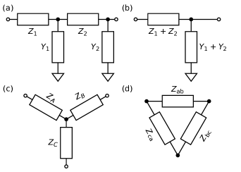
For Sec. V.2, we summarize the swapping conditions between series and shunt elements. Consider a unit cell, as shown in Fig. 19(a). When the shunt current is small, we can swap the positions of series and shunt elements and obtain a unit cell, as shown in Fig. 19(b). To justify this transformation, we use the Y– transformation, which converts the Y circuit [Fig. 19(c)] into the circuit [Fig. 19(d)]. The circuit parameters are related through the following equations:
| (129) | ||||
| (130) | ||||
| (131) |
Now, set , , and . Assuming , we obtain and . Then, the position of the unit cell is replaced, and we can justify the approximation. Considering the dual circuit, gives another condition.
References
- Enoch [2006] J. M. Enoch, History of mirrors dating back 8000 years, Optom. Vis. Sci. 83, 775 (2006).
- Veselago [1968] V. G. Veselago, The Electrodynamics of Substances with Simultaneously Negative Values of and , Sov. Phys. Uspekhi 10, 509 (1968).
- Pendry [2000] J. B. Pendry, Negative Refraction Makes a Perfect Lens, Phys. Rev. Lett. 85, 3966 (2000).
- Caloz and Itoh [2006] C. Caloz and T. Itoh, Electromagnetic Metamaterials: Transmission Line Theory and Microwave Applications (John Wiley & Sons, Hoboken, 2006).
- Solymar and Shamonina [2009] L. Solymar and E. Shamonina, Waves in Metamaterials (Oxford University Press, Oxford, 2009).
- Shelby et al. [2001] R. A. Shelby, D. R. Smith, and S. Schultz, Experimental verification of a negative index of refraction, Science 292, 77 (2001).
- Sarid and Challener [2010] D. Sarid and W. Challener, Modern Introduction to Surface Plasmons (Cambridge University Press, Cambridge, 2010).
- Sarkar et al. [2017] T. K. Sarkar, M. N. Abdallah, M. Salazar-Palma, and W. M. Dyab, Surface Plasmons-Polaritons, Surface Waves, and Zenneck Waves: Clarification of the terms and a description of the concepts and their evolution, IEEE Antennas Propag. Mag. 59, 77 (2017).
- Maier [2007] S. A. Maier, Plasmonics: Fundamentals and Applications (Springer, New York, 2007).
- Asbóth et al. [2016] J. K. Asbóth, L. Oroszlány, and A. Pályi, A Short Course on Topological Insulators: Band Structure and Edge States in One and Two Dimensions (Springer, Cham, 2016).
- Vanderbilt [2018] D. Vanderbilt, Berry Phases in Electronic Structure Theory: Electric Polarization, Orbital Magnetization and Topological Insulators (Cambridge University Press, Cambridge, 2018).
- Bliokh et al. [2019] K. Y. Bliokh, D. Leykam, M. Lein, and F. Nori, Topological non-Hermitian origin of surface Maxwell waves, Nat. Commun. 10, 580 (2019).
- Yang et al. [2020] F. Yang, S. Ma, K. Ding, S. Zhang, and J. B. Pendry, Continuous topological transition from metal to dielectric, Proc. Natl. Acad. Sci. USA 117, 16739 (2020).
- Su et al. [1979] W. P. Su, J. R. Schrieffer, and A. J. Heeger, Solitons in Polyacetylene, Phys. Rev. Lett. 42, 1698 (1979).
- Su et al. [1980] W. P. Su, J. R. Schrieffer, and A. J. Heeger, Soliton excitations in polyacetylene, Phys. Rev. B 22, 2099 (1980).
- Schindler [2020] F. Schindler, Dirac equation perspective on higher-order topological insulators, J. Appl. Phys. 128, 221102 (2020).
- Jackiw and Rebbi [1976] R. Jackiw and C. Rebbi, Solitons with fermion number 1/2, Phys. Rev. D 13, 3398 (1976).
- Stratton [1941] J. A. Stratton, Electromagnetic Theory (McGraw-Hill, New York, 1941).
- Jackson [1998] J. D. Jackson, Classical Electrodynamics, 3rd ed. (John Wiley & Sons, Hoboken, 1998).
- Bergholtz et al. [2021] E. J. Bergholtz, J. C. Budich, and F. K. Kunst, Exceptional topology of non-Hermitian systems, Rev. Mod. Phys. 93, 015005 (2021).
- Davanço et al. [2007] M. Davanço, Y. Urzhumov, and G. Shvets, The complex Bloch bands of a 2D plasmonic crystal displaying isotropic negative refraction, Opt. Express 15, 9681 (2007).
- Parisi et al. [2012] G. Parisi, P. Zilio, and F. Romanato, Complex Bloch-modes calculation of plasmonic crystal slabs by means of finite elements method, Opt. Express 20, 16690 (2012).
- Miyamaru et al. [2021] F. Miyamaru, C. Mizuo, T. Nakanishi, Y. Nakata, K. Hasebe, S. Nagase, Y. Matsubara, Y. Goto, J. Pérez-Urquizo, J. Madéo, and K. M. Dani, Ultrafast Frequency-Shift Dynamics at Temporal Boundary Induced by Structural-Dispersion Switching of Waveguides, Phys. Rev. Lett. 127, 053902 (2021).
- Note [1] A movie illustrating magnetic-field dynamics near a temporal boundary is provided as an ancillary file in arXiv.
- Keller [1964] J. B. Keller, A Theorem on the Conductivity of a Composite Medium, J. Math. Phys. 5, 548 (1964).
- Dykhne [1971] A. M. Dykhne, Conductivity of a Two-dimensional Two-phase System, Sov. Phys. JETP 32, 63 (1971).
- Mendelson [1975] K. S. Mendelson, A theorem on the effective conductivity of a two-dimensional heterogeneous medium, J. Appl. Phys. 46, 4740 (1975).
- Nakata et al. [2019] Y. Nakata, Y. Urade, and T. Nakanishi, Geometric Structure behind Duality and Manifestation of Self-Duality from Electrical Circuits to Metamaterials, Symmetry 11, 1336 (2019).
- Guillemin [1957] E. A. Guillemin, Synthesis of Passive Networks: Theory and Methods Appropriate to the Realization and Approximation Problems (John Wiley & Sons, New York, 1957).
- Wing [2010] O. Wing, Classical Circuit Theory (Springer, New York, 2010).
- Ashcroft and Mermin [1976] N. W. Ashcroft and N. D. Mermin, Solid State Physics (Holt, Rinehart and Winston, New York, 1976).
- Note [2] In particular, a CRLH transmission line has mirror symmetry with respect to or , as described in the effective model of Fig. 14.
- Xiao et al. [2014] M. Xiao, Z. Q. Zhang, and C. T. Chan, Surface Impedance and Bulk Band Geometric Phases in One-Dimensional Systems, Phys. Rev. X 4, 021017 (2014).
- Collin [1992] R. E. Collin, Foundations for Microwave Engineering, 2nd ed. (McGraw-Hill, New York, 1992).
- Bamberg and Sternberg [1990] P. Bamberg and S. Sternberg, A Course in Mathematics for Students of Physics 2 (Cambridge University Press, Cambridge, 1990).
- Nakata et al. [2012] Y. Nakata, T. Okada, T. Nakanishi, and M. Kitano, Circuit model for hybridization modes in metamaterials and its analogy to the quantum tight-binding model, Phys. Status Solidi B 249, 2293 (2012).