Stress-Tuned Optical Transitions in Layered 1T-MX2 (M= Hf, Zr, Sn; X= S, Se) Crystals
Abstract
Optical measurements under externally applied stresses allow us to study the materials’ electronic structure by comparing the pressure evolution of optical peaks obtained from experiments and theoretical calculations. We examine the stress-induced changes in electronic structure for the thermodynamically stable 1T polytype of selected MX2 compounds (M=Hf, Zr, Sn; X=S, Se), using the density functional theory. We demonstrate that considered 1T-MX2 materials are semiconducting with indirect character of the band gap, irrespective to the employed pressure as predicted using modified Becke–Johnson potential. We determine energies of direct interband transitions between bands extrema and in band-nesting regions close to Fermi level. Generally, the studied transitions are optically active, exhibiting in-plane polarization of light. Finally, we quantify their energy trends under external hydrostatic, uniaxial, and biaxial stresses by determining the linear pressure coefficients. Generally, negative pressure coefficients are obtained implying the narrowing of the band gap. The semiconducting-to-metal transition are predicted under hydrostatic pressure. We discuss these trends in terms of orbital composition of involved electronic bands. In addition, we demonstrate that the measured pressure coefficients of HfS2 and HfSe2 absorption edges are in perfect agreement with our predictions. Comprehensive and easy-to-interpret tables containing the optical features are provided to form the basis for assignation of optical peaks in future measurements.
Miłosz Rybak1 ![]() ,
Tomasz Woźniak1,∗
,
Tomasz Woźniak1,∗ ![]() ,
Magdalena Birowska2
,
Magdalena Birowska2 ![]() ,
Filip Dybała1,
Alfredo Segura3,
Konrad J. Kapcia4,5
,
Filip Dybała1,
Alfredo Segura3,
Konrad J. Kapcia4,5 ![]() ,
Paweł Scharoch1 and
Robert Kudrawiec1
,
Paweł Scharoch1 and
Robert Kudrawiec1
1 Department of Semiconductor Materials Engineering, Faculty of Fundamental Problems of Technology Wrocław University of Science and Technology, Wybrzeże Wyspiańskiego 27, 50-370 Wrocław, Poland; milosz.rybak@pwr.edu.pl (M.R.); filip.dybala@pwr.edu.pl (F.D.); pawel.scharoch@pwr.edu.pl (P.S.); robert.kudrawiec@pwr.edu.pl (R.K.)
2 Institute of Theoretical Physics, Faculty of Physics, University of Warsaw, Pasteura St. 5, 02-093 Warsaw, Poland; birowska@fuw.edu.pl
3 Departamento de Física Aplicada-ICMUV, Malta-Consolider Team, Universitat de València, 46100 Burjassot, Spain; alfredo.segura@uv.es
4 Institute of Spintronics and Quantum Information, Faculty of Physics, Adam Mickiewicz University in Poznań, ul. Uniwersytetu Poznańskiego 2, 61-614 Poznań, Poland; konrad.kapcia@amu.edu.pl
5 Center for Free-Electron Laser Science CFEL, Deutsches Elektronen-Synchrotron DESY, Notkestr. 85, 22607 Hamburg, Germany
* correspondence: tomasz.wozniak@pwr.edu.pl
Keywords MX2 DFT bulk band structure pressure coefficients transition metal dichalcogenides
1 Introduction
Among the large family of van der Waals (vdW) crystals, transition metal dichalcogenides (TMDs) have attracted a great deal of interest owing to their unique combination of direct band gap, significant spin–orbit coupling and exceptional electronic and mechanical properties, making them attractive for both fundamental studies and applications [1, 2]. In particular, their semiconducting nature opens a door to potential optoelectronic, photonic and sensing devices such as light emitting diodes, microlasers, solar cells, transistors or light detectors [3, 4, 5, 6].
Optoelectronic properties of vdW materials can be tuned by multiple external factors. One of them is an effective strain engineering. Recent theoretical and experimental reports have demonstrated flexible control over their electronic states via applying external strains [7, 8, 9]. For instance, applying an uniaxial tensile strain to monolayer of MoS2 may result in direct-to-indirect band gap transition [10], whereas applying a biaxial strain gives rise to a semiconductor-to-metal phase transition [11]. Meanwhile, the prominent mechanical strength of TMDs [12], compared with conventional 3D semiconductors, allows to use large strains for band structure engineering. For instance, combined studies by means of density functional theory (DFT) calculations and atomic force microscopy measurements have reported that the fracture stress of a freely suspended MoS2 [12, 13] approaches the theoretical limit of this quantity for defect-free elastic crystal (one-ninth its Young’s modulus) [14]. In addition, numerous nondestructive optical techniques, including Raman, absorption, photoreflectance, and photoluminescence experiments, can be readily employed to quantitatively determine strain-tuned optical properties. In addition, high-pressure measurements are highly desirable for detailed band structure information as well as give useful benchmark to test DFT calculations. Such techniques also provide a direct way to probe interlayer interaction in the layered structures. In particular, recent experimental reports have demonstrated that the energies of various optical transitions in TMDs exhibit significant pressure dependence [15, 16, 17, 18], which allows for the identification of the optical peaks, making them attractive for applications in pressure-sensing devices [19, 20, 21]. Generally, the unique mechanical flexibility and strength of TMDs make them an ideal platform for band gap engineering by strain, thus, enabling enhancement of their optical properties.
The chemical formula of hexagonal TMDs is MX2, where M stands for a transition metal element, and X is a chalcogene element (S, Se or Te). TMDs exhibit several structural polytypes of which two most common are trigonal prismatic (2H) and octahedral (1T) ones (see Figure 1). The difference between 2H and 1T polytypes can be viewed in different arrangement of atomic planes sequence within the monolayer. Namely, 2H polytype corresponds to an ABA arrangement, whereas 1T polytype is characterised by ABC sequence order [22]. Although 2H polytype of TMDs, based on Mo and W, have been extensively studied, the octahedral 1T MX2 compounds containing the M=Hf, Zr and Sn, X=S, Se elements have been less examined. The latter ones are indirect-gap semiconductors with band gaps ranging from visible to near-infrared wavelengths [23]. The earlier studies on 1T-MX2 compounds have predicted very high electron mobility and sheet current density in HfS2, superior to MoS2 [24, 25], which makes ultrathin HfS2 phototransistors appealing for optoelectronics [26]. Thin SnSe2 flakes were shown to exhibit high photoresponsivity [27]. ZrS2 nanosheets were found suitable as anodes for sodium ion batteries [28]. These findings motivate further studies of electronic properties of 1T-MX2 crystals in 1L and bulk form. Despite some works reporting pressure evolution of Raman spectra [29, 30, 31], as well as X-ray diffraction and transport measurements [32], optical measurements under pressure are largely missing for 1T-MX2 compounds.
In this work, we systematically investigate the impact of external stress on the basic features of the band structure of MX2 (M=Hf, Zr, Sn; X=S, Se) in the 1T bulk polytype by DFT calculations. For each compound, we identify the dominant direct electronic transitions in BZ. As the structural anisotropy of in-plane and out-of plane directions in layered systems may result in different response to the strain, we study the evolution of the band structure upon applying stress types that are most frequently realized in experiments, i.e., compressive isotropic (hydrostatic), biaxial, and uniaxial stress. We quantify the energy trend for each transition between ambient and band gap closing pressure by determining the linear pressure coefficients. In addition, we examine the effect of light polarization for optically active direct transitions using dipole selection rules. Our predicted pressure coefficients and polarization of transitions can serve for identification of the features in measured optical spectra. Meanwhile, we explain the observed chemical trends by the orbital composition of electronic bands involved in the transitions. Finally, we compare our calculated results to the pressure trends of absorption edges positions measured in HfS2 and HfSe2 crystals, finding an excellent agreement. It corroborates that our adopted computational strategy is accurate at the quantitative level.
2 Methods and Materials
The DFT calculations have been performed in Vienna Ab Initio Simulation Package [33]. The electron-ion interaction was modeled using projector-augmented-wave technique [34]. In the case of tin (Sn) atom, the 4d10 states were included in valence shell, for hafnium and zircon, additional s states were taken (4s2 for Zr, 5s2 for Hf). The Perdew–Burke–Ernzerhof (PBE) [35] exchange-correlation (XC) functional was employed. A plane-wave basis cutoff of 500 eV and a Monkhorst-Pack [36] k-point grid for BZ integrations were set. These values assured the convergence of the lattice constants and the electronic gaps were within precision of 0.001 Å and 0.001 eV, respectively. A Gaussian smearing of 0.02 eV was used for integration in reciprocal space. It is well known that standard exchange correlation functionals are insufficient to describe a non-local nature of dispersive forces, crucial to obtain a proper interlayer distance for layered structures [37, 38]. Thus, the semi-empirical Grimme’s correction with Becke–Johnson damping (D3-BJ) [39] was employed to properly describe the weak vdW forces. The spin–orbit (SO) interaction was taken into account.
It is well established that the standard approximations to the XC functional lead to a severe underestimation of the electronic band gap and the lack of inclusion excitonic effects. In this regard, DFT is inaccurate for identification of optical transitions based on their absolute energy values. This issue can be partly improved by using more advanced techniques such as hybrid functionals or GW method [40, 41], but their computational costs often make the calculations unfeasible for systems containing more than few atoms. The modified Becke–Johnson (mBJ) potential is an alternative approach to improve the band gaps with relatively low computational cost [42, 43, 44]. Recent report shave shown that mBJ provides reasonable results for identifying the optical transitions in ReS2 and ReSe2 bulk crystals [16]. It also yields pressure coefficients of optical transitions in excellent agreement with experimental values [15, 45]. Therefore, we employ mBJ potential for band structure calculations, on top of the optimized geometry obtained within the PBE+D3-BJ+SO approach. The direct interband momentum matrix elements were computed from the wave function derivatives using density functional perturbation theory [46].
3 Results
3.1 Theoretical Analysis
We start our research by considering the geometry and electronic structure for the unstrained systems. The optimized lattice parameters, provided in Table 1, are in perfect agreement with experimental values. Similarly to 2H-TMDs, lattice constants are mostly governed by chalcogene atoms [15]. As it is expected for heavier atoms, the selenium (Se) compounds possess larger lattice parameters than sulfur (S) ones. The electronic band structures calculated under ambient conditions are presented in Figure 2. The band edges are located at the same high symmetry k-points for all studied systems. Namely, the valence band maximum (VBM) and conduction band minimum (CBM) are located at and k-points, respectively. Note that the VBM of SnSe2 at ambient pressure is not located exactly at point, but between the and K points (on the -M path the local maximum is 2 meV lower). Under biaxial stress the VBM shifts to A point, but under hydrostatic and uniaxial stress the position and shape of VBM remain unchanged. This type of pressure behavior has already been observed in InSe crystals, where VBM exhibits toroidal shape [47, 48]. The toroidal shape has consequences in transport and optical properties and would require further investigations, which are beyond the scope of our work. The calculated fundamental gaps exhibit indirect character with values systematically lower by 30–50 with respect to experimental values (see Table 1). The systems containing Se atoms exhibit reduced size of the energy gaps in comparison to S-containing systems.
The underestimation of the band gap is related to the geometrical structure—a better agreement is obtained with the use of experimental lattice constants, as shown in Ref. [49] and discussed in Appendix B for ZrSe2. In our study, we focus, however, not on the absolute value of the band gap, but rather on the pressure dependence of optical transitions, which requires a full optimization of geometry. Further, the discrepancies between theoretical and experimental bands gaps stem from the systematic underestimation of the band gap and the lack of including excitonic effects in our theoretical approach. On the other hand, the quasi-two-dimensional character of layered crystal leads to exciton binding energies on the order of tens or hundreds of meV [50, 51, 52, 53, 54], which redshifts the optical energies from their band-to-band values. Incidentally, it can improve the agreement with experiments, but this is fortuitous result and strongly material-dependent. In contrast to the absolute energy of transition, variation of its energy with respect to pressure, quantified by a linear pressure coefficient, demonstrates to be in good agreement with measured value [15, 16, 17]. Additionally, the dependence of the exciton binding energies upon the pressure can be neglected, whenever the exciton binding energy is much smaller than the transition energy [45, 55]. Aforementioned suggest that the pressure coefficients obtained using mBJ might provide reasonable values and enable proper identification of the measured optical peaks on a quantitative level. Therefore, in order to compare the optical experimental results with our theoretical outcomes, the pressure coefficients are computed.
| System | (Å) | (Å) | (eV) | (Å) | (Å) | (eV) |
|---|---|---|---|---|---|---|
| HfS2 | 3.59 | 5.75 | 1.50 | 3.63 [56] | 5.86 [56] | 1.96 [57], 1.80 [58], 1.87 [59] |
| HfSe2 | 3.70 | 6.08 | 0.71 | 3.67 [56] | 6.00 [56] | 1.13 [57], 1.15 [58] |
| ZrS2 | 3.63 | 5.72 | 1.12 | 3.66 [57] | 5.82 [57] | 1.68 [57], 1.70[60], 1.78 [61] |
| ZrSe2 | 3.74 | 6.04 | 0.33 | 3.77 [57] | 6.14 [57] | 1.20 [60], 1.10 [62], 1.18 [63] |
| SnS2 | 3.67 | 5.80 | 2.14 | 3.65 [64] | 5.90 [64] | 2.88 [65] |
| SnSe2 | 3.84 | 6.00 | 1.10 | 3.82 [64] | 6.14 [64] | 1.63 [65] |
Although structural phase transitions under pressure were reported for our compounds [31, 30, 66, 67, 68, 69], they are out of the scope of this work and we consider only the 1T phase under hydrostatic pressures up to metallization limit. In our mBJ-PBE+SO calculations they occur at pressures of: 266 kbar for SnS2, 188 kbar for HfS2, 128 kbar for ZrS2, 84 kbar for SnSe2, 65 kbar for HfSe2 and 26 kbar for ZrSe2. We also apply uniaxial and biaxial stresses, as depicted on Figure 4, which result from reducing the lattice parameters by up to 8% (see Appendix B). Figure 3 presents the band structures of HfS2 and SnSe2 under hydrostatic, uniaxial, and biaxial stress, as representatives of (Hf,Zr)X2 and SnX2 groups. Note, that the indirect character of the band gaps is preserved, irrespective of the pressure applied. The band edges positions are located at the same k-points as for unstrained samples, except for SnX2 systems under hydrostatic pressure, where CBM moves from L to M point, and biaxial strains, where VBM moves from to A point. Note that, the application of compressive uniaxial strains result in reduction in the band gaps. Notably, the impact of hydrostatic or biaxial pressures is non-trivial and more complicated. In particular, for SnX2 compounds, the biaxial stresses initially increase the energy gap and move the VBM from to A point (see Figure 3b and the Appendix B for a detailed discussion).
On the basis of the calculated electronic band structures, we identify direct electronic transitions with energies below 4.5 eV that might be optically active. For that, we calculate the energy differences between three uppermost valence bands (VB, VB-1, and VB-2) and three lowermost conduction bands (CB, CB+1, and CB+2) and plot them along the k-path, as presented in Figure 4c,d. The minima and plateaus in these plots denote the regions of BZ, where transitions occur between bands extrema at high-symmetry k-points or between parallel bands between high-symmetry k-points, called band-nesting regions. Both types of transitions contribute to van Hove’s singularities, that give rise to measurable optical signal. Figure 4c,d reveal multiple of such transitions in HfS2 and SnSe2. Additionally, in order to be optically active a transition must have a finite dipole strength, or intensity. Their calculated values are presented in Figure 4e,f, distinguishing the in-plane and out-of-plane components. In case the former (latter) one has a non-zero value, the emitted light propagates perpendicular (parallel) to the layers’ plane. Basing on these two conditions, we identify the optically active transitions in all studied compounds and depict the exemplary ones for HfS2 and SnSe2 with arrows in Figure 4a,b.
A significant difference between the systems containing transition metal (Hf, Zr) compared to the -block metal (Sn) is visible in the orbital composition of their conduction bands. The lack of the -type orbitals close to the Fermi level for Sn compounds substantially affects the curvature of the bands. Note that, for SnS2 and SnSe2 systems CBM is separated from other conduction bands by several hundred meV (see Figure 2a,b). Such separation reflects an intermediate character of the CBM, thus in turn, significantly decreases the number of optical transitions potentially visible in experiments. In particular, two transitions with highest intensities and the different polarization of light are located at (from VB to CB, out-of plane polarization) and M (from VB to CB+1, in-plane polarization) k-points, respectively, (see Figure 4f,b). However, the latter one is less plausible due to much higher energy difference. Considering the Hf, Zr contained systems, their conduction bands are mainly composed of states, and many bands appeared in CB, resulting in a higher number of plausible transitions (see Appendix D).
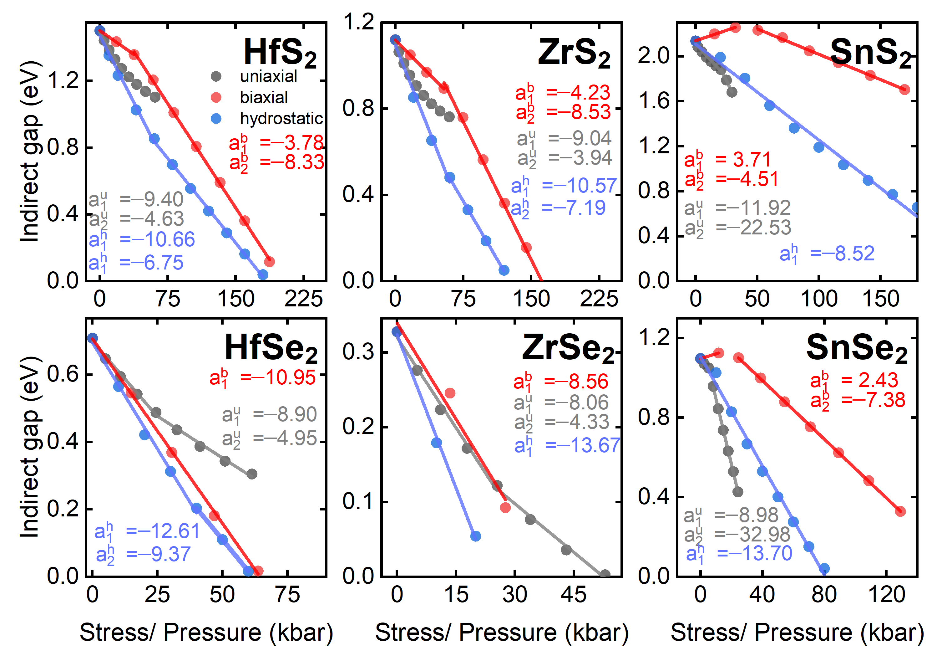
After selecting the direct transitions at high symmetry points and band-nesting regions with non-zero intensities, we discuss the pressure coefficients assigned to them and collected in Table 2. Note that, the transition energies exhibit nonlinear trends in the whole pressure range, as exemplified on Figure 5a,c for VB-CB transition in HfS2 and SnSe2. Thus, for each compound we divide the whole pressure range into three ranges, denoted I, II, and III, where the energy trends are approximately linear (for the complete list see Table 3). Figure 5b,d present the dispersion of the pressure coefficient for VB-CB transition in HfS2 and SnSe2. In HfS2, the pressure coefficients in II and III are similar and significantly different from I at , K, L, and H points. In SnSe2 the differences are even larger. For example, the VB-CB transition at exhibits a negative pressure dependence for low pressures (0–25 kbar). In range II (25–60 kbar) the energy is nearly constant and increases at higher pressures (>60 kbar).
The five lowermost optically active transitions for each compound, are collected in Table 2. The full list of all possible transitions up to 4.5 eV upon various stresses, with corresponding pressure coefficient are presented in Tables 4–7. Most of the selected transitions are located at high symmetry k-points, with a few band-nesting transitions present on -A and A-L paths. Most of transitions exhibit in-plane polarization of the light. The Se-based compounds display higher pressure coefficients than S-based ones. In particular, for the lowermost optical transition the uniaxial coefficients have in the former ones have at least two times larger absolute values than in the latter ones.
The fundamental difference between the systems containing transition metal atoms and Sn atoms is observed in the sign of pressure coefficients. For the first ones, most of the predicted pressure coefficients are negative, whereas for the systems with Sn atoms, the positive values are obtained in the case of hydrostatic and biaxial stresses (see Figures 2 and 6). In addition for SnX2 the largest pressure coefficients are obtained for uniaxial stresses (one order of magnitude larger than the rest ones), while for the rest structures it is not conclusive.
3.2 Comparison with Experiment
To benchmark our results, we compare them to the pressure trends of absorption edge positions measured in HfS2 and HfSe2. For that purpose the commercial HfS2 and HfSe2 crystals were used, grown using the state-of-art flux zone technique at 2D Semiconductors company. In order to measure the pressure dependence of absorption spectra, crystals were exfoliated to bulk-like flakes and enclosed in a diamond anvil cell (DAC). A helium-filled membrane was used to control the thrust on the diamonds and the pressure inside the chamber. The value of pressure was determined by measuring the red shift of R1 photoluminescence line from ruby spheres using the high resolution Ocean Optics HR2000+ fiber spectrometer with 1800 g/mm grating and a silicon CCD detector. Light from standard halogen lamp was focused onto the sample with reflective objectives. The absorption spectra from the sample were measured by a second spectrometer of the same type but equipped with 300 g/mm grating.
Figure 6a,b show the pressure dependence of absorption spectra measured at room temperature for HfS2 and HfSe2, respectively. In order to extract the absorption edge, the square of absorption was plotted and extrapolated to zero. The obtained pressure dependence of absorption edge is plotted by solid circles in Figure 6c,d for HfS2 and HfSe2, respectively, together with the linear fit. The respective pressure coefficients are equal to 5.13 and 7.89 meV/kbar. According to theoretical calculations the observed absorption edge can be attributed to the direct optical transition at the point of Brillouin zone. The pressure coefficient for this transition in HfS2 and HfSe2 determined from DFT are equal, respectively, to 5.49 and 7.34 meV/kbar. Note, that these theoretical values are different than those collected in Table 2, due to different pressure ranges for linear fitting. The experimental and theoretical values are in excellent agreement, confirming a quantitative accuracy of our calculations. Basing on that we predict, with high level of credibility, that it applies also to other compounds, not investigated experimentally yet.
4 Summary
This work reports an extensive DFT investigation of band structure evolution and electronic features upon applying various pressures for the bulk MX2 compounds (M=Hf, Zr, Sn; X=S, Se) in 1T polytype. We study the trends of the fundamental indirect band gap and direct transitions energies upon application of hydrostatic, uniaxial and biaxial stresses, up to semiconductor-to-metal transition. We provide the values of pressure coefficients in the ranges of linear behavior of transitions energies. Additionally, dipole strengths and polarizations of direct transitions are computed. The observed chemical trends are discussed in terms of orbital composition of involved electronic bands. In general, the negative pressure coefficients have been determined, except the (M=Sn; X=Se,S) structures under hydrostatic and biaxial stresses. The largest pressure coefficients are predicted under uniaxial stresses for Sn containing structures. We compare the calculated pressure coefficients to the experimental values for the absorption edges of HfS2 and HfSe2, obtaining and excellent agreement. It corroborates, that our computational strategy (PBE+D3-BJ+SO for geometry optimization, mBJ+SO for band structure calculations), yields a quantitative precision for identification of optical peaks in 1T-MX2, based on their pressure evolution. Our work provides easy-to-interpret tables with electronic band structure features under applying stress. Such results provide an indispensable and complete aid for materials characterization, as they enable assignment of measured optical peaks to specific transitions in the electronic band structure.
| Point | v | c | E | |||||||||||
|---|---|---|---|---|---|---|---|---|---|---|---|---|---|---|
| L | VB | CB | 2.076 | 21 | 11 | 7.61 | 5.45 | 5.05 | 5.16 | 2.91 | 1.72 | 5.49 | 6.99 | 7.68 |
| VB | CB | 2.448 | 0 | 3 | 6.64 | 3.56 | 3.78 | 12.83 | 9.51 | 8.00 | 1.08 | -6.29 | 9.26 | |
| n.A | VB | CB | 2.687 | 67 | 0 | 4.19 | 1.71 | 0.96 | 9.16 | 7.96 | 7.03 | 1.71 | 2.07 | 2.98 |
| VB-1 | CB | 2.690 | 66 | 0 | 0.87 | 0.66 | 0.66 | 0.21 | 0.14 | 0.25 | 1.63 | 6.74 | 9.75 | |
| L | VB-1 | CB | 2.781 | 30 | 2 | 2.63 | 1.26 | 0.94 | 1.06 | 2.63 | 3.50 | 6.89 | 4.89 | 4.98 |
| VB | CB | 1.699 | 52 | 0 | 9.04 | 6.57 | 5.79 | 10.77 | 8.70 | 7.94 | 8.15 | 13.52 | 14.72 | |
| VB-1 | CB | 1.716 | 5 | 5 | 4.02 | 4.06 | 4.79 | 0.84 | 1.03 | 1.13 | 4.34 | 12.03 | 13.93 | |
| L | VB | CB | 1.758 | 14 | 14 | 10.18 | 8.11 | 6.97 | 3.32 | 2.02 | 1.26 | 8.63 | 9.98 | 9.97 |
| VB-1 | CB+1 | 1.811 | 22 | 0 | 2.92 | 2.33 | 1.96 | 0.34 | 0.71 | 0.94 | 0.40 | 2.10 | 2.58 | |
| A | VB | CB | 1.962 | 68 | 0 | 1.32 | 1.02 | 0.79 | 4.02 | 3.63 | 3.57 | 3.06 | 3.65 | 4.49 |
| VB | CB+1 | 1.777 | 4 | 0 | 5.41 | 2.53 | 1.69 | 11.51 | 8.27 | 7.22 | 3.73 | 3.09 | 2.86 | |
| L | VB | CB | 1.949 | 10 | 20 | 7.64 | 5.70 | 5.30 | 5.17 | 2.70 | 1.52 | 1.68 | 1.01 | 0.60 |
| VB-1 | CB+2 | 2.073 | 11 | 0 | 4.41 | 4.44 | 4.10 | 3.65 | 4.20 | 4.69 | 1.18 | 1.57 | 1.86 | |
| VB-2 | CB+1 | 2.164 | 41 | 0 | 1.37 | 0.96 | 0.78 | 0.16 | 0.23 | 0.40 | 0.05 | 0.09 | 0.16 | |
| A | VB | CB | 2.209 | 61 | 0 | 1.36 | 1.11 | 1.13 | 2.96 | 2.67 | 2.63 | 0.96 | 1.00 | 1.04 |
| VB | CB+1 | 1.151 | 14 | 0 | 6.76 | 3.50 | 2.46 | 8.29 | 5.75 | 4.92 | 2.92 | 3.48 | 0.60 | |
| n.A | VB | CB | 1.252 | 54 | 0 | 5.31 | 2.36 | 1.46 | 10.08 | 7.87 | 7.06 | 3.62 | 10.30 | 12.88 |
| VB-1 | CB | 1.252 | 53 | 0 | 2.87 | 2.88 | 5.39 | 1.34 | 1.38 | 1.34 | 1.65 | 12.33 | 9.91 | |
| L | VB | CB | 1.320 | 23 | 6 | 10.03 | 7.75 | 7.10 | 3.25 | 1.86 | 0.98 | 9.22 | 10.43 | 10.32 |
| A | VB | CB | 1.460 | 60 | 0 | 1.64 | 1.33 | 0.89 | 4.46 | 3.91 | 3.87 | 2.94 | 3.10 | 3.34 |
| VB | CB | 2.595 | 0 | 61 | 4.73 | 0.22 | 1.28 | 28.59 | 25.78 | 24.78 | 13.08 | 1.03 | 1.09 | |
| L | VB-2 | CB | 3.786 | 3 | 35 | 2.20 | 4.21 | 8.71 | 4.56 | 1.89 | 0.30 | 4.32 | 1.38 | 2.14 |
| H | VB | CB | 3.871 | 4 | 0 | 3.01 | 3.00 | 2.85 | 2.63 | 3.11 | 3.71 | 3.84 | 2.21 | 1.42 |
| H | VB-1 | CB | 3.889 | 7 | 0 | 2.89 | 3.01 | 2.85 | 2.48 | 2.99 | 3.60 | 3.78 | 2.16 | 1.38 |
| K | VB | CB | 3.953 | 20 | 0 | 3.87 | 2.52 | 1.65 | 1.38 | 0.96 | 0.55 | 2.64 | 1.52 | 0.96 |
| VB | CB | 1.446 | 8 | 67 | 5.31 | 0.15 | 1.17 | 34.07 | 31.48 | 32.20 | 11.54 | 0.14 | 2.98 | |
| VB-2 | CB | 1.959 | 112 | 0 | 3.18 | 8.11 | 8.06 | 6.45 | 5.74 | 2.35 | 4.45 | 0.08 | 2.75 | |
| H | VB | CB | 2.969 | 3 | 3 | 2.74 | 3.00 | 2.56 | 4.41 | 5.21 | 6.68 | 4.16 | 2.25 | 1.21 |
| L | VB-2 | CB | 2.986 | 14 | 14 | 4.16 | 4.95 | 4.96 | 1.36 | 5.21 | 8.35 | 1.66 | 2.95 | 4.30 |
| K | VB | CB | 3.072 | 22 | 0 | 4.17 | 3.24 | 1.43 | 0.47 | 0.52 | 1.76 | 2.73 | 1.42 | 0.69 |
Author contributions
Conceptualization, M.R. and T.W.; methodology, M.R., T.W., and A.S.; software, M.R.; validation, M.B.; formal analysis, M.R. and F.D.; investigation, M.R. and F.D.; resources, M.R., A.S., and K.J.K.; data curation, M.R. and F.D.; writing—original draft preparation, M.R.; writing—review and editing, T.W., M.B., and P.S; visualization, M.R.; supervision, R.K., P.S., and K.J.K.; project administration, M.R., R.K., P.S., and K.J.K.; funding acquisition, R.K. All authors have read and agreed to the published version of the manuscript.
Funding
K.J.K. thanks the Polish National Agency for Academic Exchange for funding in the frame of the Bekker programme (PPN/BEK/2020/1/00184). K.J.K. is also grateful for the funding from the scholarships of the Minister of Science and Higher Education (Poland) for outstanding young scientists (2019 edition, No. 821/STYP/14/2019).
Acknowledgments
M.R., T.W., K.J.K., P.S., and R.K. thank Przemysław Piekarz for helpful discussions. M.B. acknowledges support by the University of Warsaw within the project “Excellence Initiative-Research University” programme. Access to computing facilities of PL-Grid Polish Infrastructure for Supporting Computational Science in the European Research Space and of the Interdisciplinary Center of Modeling (ICM), University of Warsaw are gratefully acknowledged. M.R. acknowledges the hospitality of the Henryk Niewodniczański Institute of Nuclear Physics (of the Polish Academy of Sciences) in Kraków during his student internship.
Appendix A Appendix Band Gap Dependence on Geometrical Parameters
Previously, a comparison of mBJ and experimental band gaps for Hf and Zr-based compounds was reported by Jiang [49]. The better agreement obtained by Jiang is related to the use of experimental geometrical parameters. In Figure 7, we compare the band structures of ZrSe2 calculated on top of geometrical structures from various optimization schemes. Depending on the scheme, band gap varies from 0.33 to 0.95 eV. Particularly, following Jiang’s approach (experimental lattice constants and relaxed atomic positions) we obtain a band gap of 0.65 eV, very close to his value of 0.68 eV. It should also be noted, that the best agreement with experimental band gap is obtained from PBE optimization without vdW correction. However, this scheme is known to fail for pressure/stress calculations [15, 29].
Appendix B Appendix Stress vs. Strain Dependencies
In order to determine the stress coefficients of the systems, the modifications of the in-plane lattice constant were made in the case of biaxial stresses, and the out-of-plane lattice constant in the case of uniaxial stresses. After optimizing the remaining degrees of freedom, the applied deformations led to non-zero stress tensor components as can be seen in Figure 8.
Analyzing the chemical trends, we see that in the case of biaxial strains the stress caused by deformation is clearly higher for sulfur-based compounds and depends mainly on chalcogene atoms, while in the case of uniaxial strains, the resulting stress is similar for sulfur and selenium, but significantly different depending on whether we have transition metal or p-block metal, which is confirmed by the values of elastic constants obtained in the literature for these systems [40, 70, 71].
Appendix C Appendix Indirect Transition
The fundamental band gaps of all the studied compounds are indirect. At ambient pressure, the VBM and CBM are located at and points, respectively. The pressure/stress behavior of the indirect band gaps is presented in Figure 9.
As in Section 3, the pressure ranges are divided into arbitrary sections, where the dependencies can be approximated linearly. Tabulated values of linear pressure coefficients with the corresponding ranges are summarized in Table 3. Only for compounds with tin there is a change of vertices from -L to -K (for SnSe2 A-K). For hydrostatic pressure, this transition takes place between 20 and 40 kbar for SnS2 and 10–20 kbar for SnSe2. For uniaxial stresses it is around 20 kbar for the sulfur compound and slightly larger 5 kbar for the material with selenium. For biaxial stresses, the discussed transition in SnS2 occurs at around 40 kbar, but for the selenium counterpart, the transition from the to L points changes into A to K already at 10 kbar. Negative values in Figure 3 mean further energy difference between these points, after exceeding band gap closing pressure.
| pressure range of (kbar) | stress range of (kbar) | stress range of (kbar) | ||||
|---|---|---|---|---|---|---|
| I | II | I | II | I | II | |
| HfS2 | [0–60] | [60–180] | [0–23.5] | [23.5–60.9] | [0–58.5] | [58.5–239.5] |
| HfSe2 | [0–40] | [40–60] | [0–24.5] | [24.5–61.3] | [0-62.9] | |
| ZrS2 | [0–60] | [60–120] | [0–23.2] | [23.2–53.01] | [0–53.8] | [53.8–169.0] |
| ZrSe2 | [0–20] | [0–25.5] | [25.5–63.5] | [0–27.56] | ||
| SnS2 | [0–180] | [0–20.6] | [20.6–29.5] | [0–32.3] | [50.5–169.8] | |
| SnSe2 | [0–80] | [0–5.26] | [8.2–25.2] | [0–11.8] | [25.6–129.2] | |
| (meV/kbar) | (meV/kbar) | (meV/kbar) | ||||
| n | I | II | I | II | I | II |
| HfS2 | 10.66 | 6.75 | 9.40 | 4.63 | 3.78 | 8.33 |
| HfSe2 | 12.61 | 9.37 | 8.90 | 4.95 | 10.95 | |
| ZrS2 | 10.57 | 7,19 | 9.04 | 3.94 | 4.23 | 8.53 |
| ZrSe2 | 13.67 | 8.06 | 3.84 | 8.56 | ||
| SnS2 | 8.52 | 11.92 | 22.53 | 3.71 | 4.51 | |
| SnSe2 | 7.19 | 13.70 | 32.98 | 2.43 | 7.38 | |
Appendix D Appendix Tables with Pressure Coefficients
The pressure coefficients of direct transitions under hydrostatic, uniaxial, and biaxial stresses for Hf, Zr, and Sn-based compounds are collected in Tables 4–7, respectively. The first column contains the position of the transition in the BZ. The next two columns indicate the valence and conduction bands between which the optical transition occurs. The ambient pressure energy and polarization of the transition are provided in fourth and fifth column. The last nine columns contain the pressure coefficients assigned for hydrostatic, uniaxial, and biaxial stress in the selected pressure ranges.
| Point | v | c | E | ||||||||||
| L | VB | CB | 2.076 | / | 7.61 | 5.45 | 5.05 | 5.16 | 2.91 | 1.72 | 5.49 | 6.99 | 7.68 |
| VB | CB | 2.448 | 6.64 | 3.56 | 3.78 | 12.83 | 9.51 | 8.00 | 1.08 | -6.29 | 9.26 | ||
| n.A | VB | CB | 2.687 | 4.19 | 1.71 | 0.96 | 9.16 | 7.96 | 7.03 | 1.71 | 2.07 | 2.98 | |
| VB-1 | CB | 2.690 | 0.87 | 0.66 | 0.66 | 0.21 | 0.14 | 0.25 | 1.63 | 6.74 | 9.75 | ||
| L | VB-1 | CB | 2.781 | / | 2.63 | 1.26 | 0.94 | 1.06 | 2.63 | 3.50 | 6.89 | 4.89 | 4.98 |
| A | VB | CB | 2.833 | 0.98 | 0.84 | 0.80 | 2.44 | 2.34 | 2.23 | 1.56 | 1.85 | 2.06 | |
| VB-2 | CB+1 | 2.842 | 1.54 | 1.06 | 1.06 | 0.26 | 0.33 | 0.54 | 0.73 | 2.32 | 2.52 | ||
| A | VB-1 | CB+1 | 2.955 | 0.86 | 0.85 | 0.85 | 2.42 | 2.37 | 2.28 | 1.85 | 1.84 | 2.18 | |
| M | VB | CB | 3.120 | 0.89 | 0.91 | 0.93 | 5.29 | 4.73 | 4.44 | 6.07 | 5.50 | 5.59 | |
| VB | CB+2 | 3.134 | 8.26 | 5.23 | 3.57 | 8.88 | 5.68 | 4.29 | 4.98 | 4.13 | 2.76 | ||
| VB-1 | CB+2 | 3.356 | 4.00 | 3.50 | 2.55 | 3.10 | 3.57 | 3.65 | 6.57 | 3.70 | 2.70 | ||
| n.AL | VB-2 | CB+1 | 3.486 | 0.03 | 1.07 | 1.38 | 6.03 | 5.59 | 5.65 | 4.10 | 2.86 | 2.07 | |
| A | VB | CB+2 | 3.841 | 0.84 | 0.44 | 0.32 | 3.97 | 3.43 | 3.16 | 3.82 | 4.60 | 5.40 | |
| A | VB-1 | CB+2 | 4.082 | 0.74 | 0.37 | 0.25 | 3.97 | 3.45 | 3.18 | 3.92 | 4.67 | 5.47 | |
| VB | CB | 1.699 | 9.04 | 6.57 | 5.79 | 10.77 | 8.70 | 7.94 | 8.15 | 13.52 | 14.72 | ||
| VB-1 | CB | 1.716 | / | 4.02 | 4.06 | 4.79 | 0.84 | 1.03 | 1.13 | 4.34 | 12.03 | 13.93 | |
| L | VB | CB | 1.758 | / | 10.18 | 8.11 | 6.97 | 3.32 | 2.02 | 1.26 | 8.63 | 9.98 | 9.97 |
| VB-1 | CB+1 | 1.811 | 2.92 | 2.33 | 1.96 | 0.34 | 0.71 | 0.94 | 0.40 | 2.10 | 2.58 | ||
| A | VB | CB | 1.962 | 1.32 | 1.02 | 0.79 | 4.02 | 3.63 | 3.57 | 3.06 | 3.65 | 4.49 | |
| VB-1 | CB+2 | 2.140 | 5.78 | 4.69 | 3.47 | 3.35 | 3.89 | 4.34 | 3.46 | 2.85 | 2.77 | ||
| VB | CB+2 | 2.161 | 10.81 | 7.20 | 4.47 | 8.26 | 5.84 | 4.72 | 7.27 | 4.35 | 3.57 | ||
| L | VB-1 | CB | 2.183 | / | 9.48 | 7.63 | 6.59 | 1.24 | 1.46 | 3.00 | 5.95 | 5.51 | 5.32 |
| VB-2 | CB | 2.256 | 5.25 | 4.32 | 4.75 | 1.68 | 0.11 | 0.64 | 3.39 | 5.52 | 5.64 | ||
| A | VB-1 | CB | 2.317 | 1.35 | 1.05 | 0.81 | 3.93 | 3.52 | 3.47 | 2.93 | 3.52 | 4.36 | |
| A | VB-1 | CB+1 | 2.318 | 1.09 | 0.86 | 0.69 | 3.79 | 3.45 | 3.44 | 2.92 | 3.07 | 2.89 | |
| VB-2 | CB+1 | 2.341 | 4.15 | 2.60 | 1.92 | 2.18 | 0.21 | 0.45 | 1.34 | 4.41 | 5.71 | ||
| M | VB | CB | 2.476 | 0.15 | 0.65 | 0.82 | 6.80 | 5.87 | 5.79 | 7.30 | 7.71 | 7.66 | |
| VB-2 | CB+1 | 2.673 | / | 7.02 | 4.96 | 3.41 | 0.83 | 2.97 | 3.85 | 2.52 | 3.66 | 5.52 | |
| A | VB | CB+2 | 2.728 | 1.41 | 0.86 | 0.54 | 5.45 | 4.57 | 4.38 | 5.38 | 7.07 | 7.29 | |
| A | VB-1 | CB+2 | 3.055 | 1.45 | 0.89 | 0.57 | 5.35 | 4.46 | 4.27 | 5.25 | 6.94 | 7.15 | |
| n.AL | VB-2 | CB | 3.433 | 2.28 | 2.00 | 1.83 | 0.26 | 0.81 | 1.32 | 2.76 | 7.23 | 7.53 |
| Point | v | c | E | ||||||||||
|---|---|---|---|---|---|---|---|---|---|---|---|---|---|
| VB | CB+1 | 1.777 | 5.41 | 2.53 | 1.69 | 11.51 | 8.27 | 7.22 | 3.73 | 3.09 | 2.86 | ||
| L | VB | CB | 1.949 | / | 7.64 | 5.70 | 5.30 | 5.17 | 2.70 | 1.52 | 1.68 | 1.01 | 0.60 |
| VB-1 | CB+2 | 2.073 | 4.41 | 4.44 | 4.10 | 3.65 | 4.20 | 4.69 | 1.18 | 1.57 | 1.86 | ||
| VB-2 | CB+1 | 2.164 | 1.37 | 0.96 | 0.78 | 0.16 | 0.23 | 0.40 | 0.05 | 0.09 | 0.16 | ||
| A | VB | CB | 2.209 | 1.36 | 1.11 | 1.13 | 2.96 | 2.67 | 2.63 | 0.96 | 1.00 | 1.04 | |
| L | VB-1 | CB+1 | 2.259 | 0.83 | 1.32 | 1.45 | 2.60 | 2.09 | 2.03 | 0.84 | 0.78 | 0.80 | |
| A | VB-1 | CB+1 | 2.299 | 1.40 | 1.15 | 1.15 | 2.93 | 2.67 | 2.64 | 0.95 | 1.00 | 1.05 |
| Point | v | c | E | ||||||||||
|---|---|---|---|---|---|---|---|---|---|---|---|---|---|
| A | VB-1 | CB+2 | 2.331 | 1.32 | 0.64 | 0.48 | 5.45 | 4.53 | 4.34 | 1.76 | 1.69 | 1.72 | |
| VB | CB+2 | 2.547 | 8.45 | 5.98 | 5.00 | 5.45 | 4.29 | 2.90 | 2.51 | 1.61 | 1.15 | ||
| M | VB | CB | 2.702 | 0.07 | 0.45 | 0.82 | 6.52 | 5.76 | 5.73 | 2.11 | 2.15 | 2.27 | |
| VB-1 | CB | 2.834 | 1.38 | 1.03 | 1.55 | 0.16 | 0.16 | 0.29 | 0.05 | 0.06 | 0.11 | ||
| VB-2 | CB+2 | 2.927 | 4.41 | 4.42 | 4.08 | 3.58 | 4.21 | 4.72 | 1.16 | 1.57 | 1.87 | ||
| M | VB-1 | CB+1 | 3.366 | 5.93 | 3.13 | 3.71 | 2.94 | 0.01 | 1.80 | 0.95 | 0.01 | 0.71 | |
| n.AL | VB-2 | CB | 3.400 | 2.42 | 0.46 | 0.35 | 6.41 | 4.89 | 4.47 | 2.07 | 1.83 | 1.77 | |
| A | VB | CB+2 | 3.486 | 1.33 | 0.64 | 0.49 | 5.47 | 4.53 | 4.34 | 1.77 | 1.69 | 1.72 | |
| M | VB-2 | CB | 3.894 | / | 1.71 | 2.81 | 2.88 | 2.25 | 2.04 | 1.70 | 0.73 | 0.76 | 0.67 |
| L | VB | CB+1 | 4.272 | 0.01 | 1.55 | 1.90 | 9.14 | 7.58 | 7.38 | 2.96 | 2.83 | 2.93 | |
| VB | CB+1 | 1.151 | 6.76 | 3.50 | 2.46 | 8.29 | 5.75 | 4.92 | 2.92 | 3.48 | 0.60 | ||
| n.A | VB | CB | 1.252 | 5.31 | 2.36 | 1.46 | 10.08 | 7.87 | 7.06 | 3.62 | 10.30 | 12.88 | |
| VB-1 | CB | 1.252 | 2.87 | 2.88 | 5.39 | 1.34 | 1.38 | 1.34 | 1.65 | 12.33 | 9.91 | ||
| L | VB | CB | 1.320 | / | 10.03 | 7.75 | 7.10 | 3.25 | 1.86 | 0.98 | 9.22 | 10.43 | 10.32 |
| A | VB | CB | 1.460 | 1.64 | 1.33 | 0.89 | 4.46 | 3.91 | 3.87 | 2.94 | 3.10 | 3.34 | |
| A | VB | CB+1 | 1.465 | 1.68 | 1.35 | 0.90 | 4.49 | 3.92 | 3.87 | 2.95 | 3.01 | 3.11 | |
| VB | CB+2 | 1.513 | 11.36 | 7.40 | 3.97 | 5.66 | 2.54 | 1.15 | 10.02 | 3.77 | 0.50 | ||
| VB-1 | CB+2 | 1.604 | 7.28 | 5.86 | 3.40 | 3.19 | 4.04 | 4.75 | 6.41 | 1.67 | 2.53 | ||
| L | VB-1 | CB | 1.653 | 9.60 | 7.59 | 6.93 | 0.65 | 2.10 | 3.65 | 6.73 | 5.97 | 5.78 | |
| VB-2 | CB+1 | 1.663 | 3.23 | 1.94 | 1.76 | 0.42 | 0.65 | 0.79 | 0.23 | 3.85 | 5.16 | ||
| A | VB-1 | CB+1 | 1.798 | 1.82 | 1.47 | 1.02 | 4.37 | 3.79 | 3.72 | 2.70 | 2.77 | 2.88 | |
| VB-2 | CB+2 | 2.031 | / | 7.83 | 5.84 | 3.27 | 3.04 | 3.86 | 4.55 | 6.87 | 3.56 | 5.06 | |
| M | VB | CB | 2.133 | 0.49 | 0.12 | 0.51 | 7.90 | 6.75 | 6.63 | 7.60 | 7.90 | 7.85 | |
| A | VB | CB+2 | 2.379 | 1.63 | 0.92 | 0.45 | 7.07 | 5.78 | 5.53 | 6.55 | 8.38 | 9.36 | |
| A | VB-1 | CB+2 | 2.663 | 1.78 | 1.05 | 0.57 | 6.95 | 5.65 | 5.37 | 6.30 | 8.13 | 9.12 | |
| L | VB-1 | CB+1 | 3.939 | 0.52 | 1.86 | 2.21 | 4.54 | 2.68 | 2.17 | 7.12 | 8.78 | 8.82 | |
| L | VB | CB+2 | 4.107 | 1.98 | 3.16 | 3.19 | 7.75 | 7.38 | 7.74 | 6.45 | 4.05 | 2.07 | |
| M | VB | CB+1 | 4.272 | 9.62 | 8.37 | 7.57 | 5.71 | 4.46 | 4.00 | 4.14 | 4.85 | 4.91 | |
| H | VB-1 | CB | 4.372 | / | 2.58 | 0.12 | 0.03 | 5.76 | 5.51 | 5.96 | 2.37 | 0.99 | 0.32 |
| L | VB-1 | CB+2 | 4.413 | 2.41 | 3.33 | 3.36 | 5.16 | 3.42 | 3.12 | 8.93 | 8.51 | 6.61 | |
| K | VB-1 | CB | 4.500 | / | 5.25 | 4.87 | 4.64 | 4.69 | 4.92 | 5.46 | 9.90 | 9.73 | 1.37 |
| Point | v | c | E | ||||||||||
| VB | CB | 2.595 | 4.73 | 0.22 | 1.28 | 28.59 | 25.78 | 24.78 | 13.08 | 1.03 | 1.09 | ||
| L | VB-2 | CB | 3.786 | / | 2.20 | 4.21 | 8.71 | 4.56 | 1.89 | 0.30 | 4.32 | 1.38 | 2.14 |
| H | VB | CB | 3.871 | 3.01 | 3.00 | 2.85 | 2.63 | 3.11 | 3.71 | 3.84 | 2.21 | 1.42 | |
| H | VB-1 | CB | 3.889 | 2.89 | 3.01 | 2.85 | 2.48 | 2.99 | 3.60 | 3.78 | 2.16 | 1.38 | |
| K | VB | Cb | 3.953 | 3.87 | 2.52 | 1.65 | 1.38 | 0.96 | 0.55 | 2.64 | 1.52 | 0.96 | |
| L | VB-1 | CB | 3.960 | 11.38 | 9.33 | 3.81 | 14.60 | 18.29 | 20.07 | 1.79 | 1.56 | 1.23 | |
| A | VB-2 | CB | 4.439 | 13.55 | 9.42 | 3.37 | 9.98 | 8.16 | 7.35 | 6.32 | 4.01 | 2.43 | |
| VB | CB | 1.446 | / | 5.31 | 0.15 | 1.17 | 34.07 | 31.48 | 32.20 | 11.54 | 0.14 | 2.98 | |
| VB-2 | CB | 1.959 | 3.18 | 8.11 | 8.06 | 6.45 | 5.74 | 2.35 | 4.45 | 0.08 | 2.75 | ||
| H | VB | CB | 2.969 | / | 2.74 | 3.00 | 2.56 | 4.41 | 5.21 | 6.68 | 4.16 | 2.25 | 1.21 |
| L | VB-2 | CB | 2.986 | / | 4.16 | 4.95 | 4.96 | 1.36 | 5.21 | 8.35 | 1.66 | 2.95 | 4.30 |
| H | VB-1 | CB | 3.056 | 2.92 | 3.12 | 2.66 | 3.91 | 4.71 | 6.15 | 4.02 | 2.13 | 1.10 | |
| K | VB | CB | 3.072 | 4.17 | 3.24 | 1.43 | 0.47 | 0.52 | 1.76 | 2.73 | 1.42 | 0.69 | |
| K | VB-1 | CB | 3.158 | 3.56 | 2.52 | 2.16 | 0.38 | 1.65 | 3.34 | 2.75 | 1.42 | 0.67 | |
| A | VB-2 | CB | 3.620 | 16.97 | 12.85 | 5.78 | 14.57 | 12.49 | 11.58 | 5.25 | 2.93 | 0.86 | |
| A | VB | CB+1 | 3.676 | 0.08 | 0.27 | 5.86 | 6.28 | 6.90 | 8.13 | 4.06 | 3.08 | 2.62 | |
| A | VB-1 | CB+1 | 3.937 | 0.01 | 0.33 | 5.92 | 6.45 | 7.13 | 8.36 | 4.29 | 3.29 | 2.83 | |
| VB-1 | CB+1 | 3.955 | 6.62 | 1.84 | 1.78 | 6.22 | 7.03 | 0.44 | 7.55 | 2.74 | 2.37 | ||
| M | VB-2 | CB | 4.092 | 16.77 | 12.96 | 11.78 | 24.12 | 24.44 | 26.34 | 2.00 | 2.70 | 3.50 | |
| K | VB-2 | CB | 4.445 | 10.08 | 6.11 | 5.83 | 25.72 | 26.06 | 29.05 | 6.28 | 3.92 | 2.70 |
References
- [1] Karim Khan, Ayesha Khan Tareen, Muhammad Aslam, Renheng Wang, Yupeng Zhang, Asif Mahmood, Zhengbiao Ouyang, Han Zhang, and Zhongyi Guo. Recent developments in emerging two-dimensional materials and their applications. Journal of Materials Chemistry C, 8:387–440, 2020.
- [2] Qiaoliang Bao and Hui Ying Hoh. 2D materials for photonic and optoelectronic applications. Elsevier, 2020.
- [3] Naifeng Li, Yue Wang, Haifeng Sun, Junjie Hu, Maoyuan Zheng, Sihao Ye, Qi Wang, Yingtao Li, Deyan He, Jiatai Wang, Guangan Zhang, and Jing Qi. Resistive switching behaviors and mechanisms of HfS2 film memory devices studied by experiments and density functional theory calculations. Applied Physics Letters, 116(6):063503, 2020.
- [4] Jinde Yin, Fangxiang Zhu, Jintao Lai, Hao Chen, Mengyu Zhang, Jiaqiang Zhang, Jintao Wang, Tingchao He, Bo Zhang, Jianping Yuan, Peiguang Yan, and Shuangchen Ruan. Hafnium sulfide nanosheets for ultrafast photonic device. Advanced Optical Materials, 7(5):1801303, 2019.
- [5] Sreedevi Gedi, Vasudeva Reddy Minnam Reddy, Babu Pejjai, Chinho Park, Chan-Wook Jeon, and Tulasi Ramakrishna Reddy Kotte. Studies on chemical bath deposited SnS2 films for Cd-free thin film solar cells. Ceramics International, 43(4):3713–3719, 2017.
- [6] Tianci Feng, Dan Zhang, Xiaohui Li, Qyyum Abdul, ZhaoJiang Shi, Jiangbo Lu, Penglai Guo, Ying Zhang, Jishu Liu, and Qi Jie Wang. SnS2 nanosheets for Er-doped fiber lasers. ACS Applied Nano Materials, 3(1):674–681, Jan 2020.
- [7] Keliang He, Charles Poole, Kin Fai Mak, and Jie Shan. Experimental demonstration of continuous electronic structure tuning via strain in atomically thin mos2. Nano Letters, 13(6):2931–2936, Jun 2013.
- [8] Hongliang Shi, Hui Pan, Yong-Wei Zhang, and Boris I. Yakobson. Quasiparticle band structures and optical properties of strained monolayer MoS2 and WS2. Phys. Rev. B, 87:155304, Apr 2013.
- [9] Hiram J. Conley, Bin Wang, Jed I. Ziegler, Richard F. Haglund, Sokrates T. Pantelides, and Kirill I. Bolotin. Bandgap engineering of strained monolayer and bilayer MoS2. Nano Letters, 13(8):3626–3630, Aug 2013.
- [10] Emilio Scalise, Michel Houssa, Geoffrey Pourtois, Valery Afanas’ev, and André Stesmans. Strain-induced semiconductor to metal transition in the two-dimensional honeycomb structure of MoS2. Nano Research, 5(1):43–48, Jan 2012.
- [11] M. Ghorbani-Asl, S. Borini, A. Kuc, and T. Heine. Strain-dependent modulation of conductivity in single-layer transition-metal dichalcogenides. Phys. Rev. B, 87:235434, Jun 2013.
- [12] Andres Castellanos-Gomez, Vibhor Singh, Herre S. J. van der Zant, and Gary A. Steele. Mechanics of freely-suspended ultrathin layered materials. Annalen der Physik, 527(1-2):27–44, 2015.
- [13] Simone Bertolazzi, Jacopo Brivio, and Andras Kis. Stretching and breaking of ultrathin mos2. ACS Nano, 5(12):9703–9709, Dec 2011.
- [14] A. A. V. I. Griffith. The phenomena of rupture and flow in solids. Philos. Trans. R. Soc. Lond. A, 221:163–198, Aug 1921.
- [15] F. Dybała, M. P. Polak, J. Kopaczek, P. Scharoch, K. Wu, S. Tongay, and R. Kudrawiec. Pressure coefficients for direct optical transitions in MoS2, MoSe2, WS2, and WSe2 crystals and semiconductor to metal transitions. Scientific Reports, 6:26663, 5 2016.
- [16] Robert Oliva, Magdalena Laurien, Filip Dybala, Jan Kopaczek, Ying Qin, Sefaattin Tongay, Oleg Rubel, and Robert Kudrawiec. Pressure dependence of direct optical transitions in ReS2 and ReSe2. npj 2D Materials and Applications, 3:20, 12 2019.
- [17] R. Oliva, T. Woźniak, F. Dybala, A. Tołłoczko, J. Kopaczek, P. Scharoch, and R. Kudrawiec. Valley polarization investigation of ges under high pressure. Physical Review B, 101, 6 2020.
- [18] R. Oliva, T. Woźniak, F. Dybala, J. Kopaczek, P. Scharoch, and R. Kudrawiec. Hidden spin-polarized bands in semiconducting 2H-MoTe2. Materials Research Letters, 8:75–81, 2 2020.
- [19] Xing Pang, Qi Zhang, Yiwei Shao, Mingjie Liu, Dongliang Zhang, and Yulong Zhao. A flexible pressure sensor based on magnetron sputtered mos2. Sensors, 21(4):1130, 2021.
- [20] Chunqing Yang, Dongzhi Zhang, Dongyue Wang, Xiaoya Chen, and Huixin Luan. Ultra-sensitive, stretchable, and bidirectional wearable strain sensor for human motion detection. J. Mater. Chem. C, 10:7076–7086, 2022.
- [21] Jaesung Lee and Philip X. L. Feng. Atomically-thin MoS2 resonators for pressure sensing. In 2014 IEEE INTERNATIONAL FREQUENCY CONTROL SYMPOSIUM (FCS), IEEE International Frequency Control Symposium, pages 276–279. IEEE; UFFC; Asia Pacific Metrol Programme; Minist Sci & Technol; NAR Labs; Instrument Technol Res Ctr; Sensors & Actuators Tech; Tsing Hua Univ, 2014.
- [22] Sajedeh Manzeli, Dmitry Ovchinnikov, Diego Pasquier, Oleg V. Yazyev, and Andras Kis. 2d transition metal dichalcogenides. Nature Reviews Materials, 2(8):17033, Jun 2017.
- [23] Inturu Omkaram, Young Ki Hong, and Sunkook Kim. Transition metal dichalcogenide photodetectors. In Pramoda Kumar Nayak, editor, Two-dimensional Materials for Photodetector, chapter 2. IntechOpen, Rijeka, 2017.
- [24] Cheng Gong, Hengji Zhang, Weihua Wang, Luigi Colombo, Robert M. Wallace, and Kyeongjae Cho. Band alignment of two-dimensional transition metal dichalcogenides: Application in tunnel field effect transistors. Applied Physics Letters, 103(5):053513, 2013.
- [25] Kai Xu, Zhenxing Wang, Feng Wang, Yun Huang, Fengmei Wang, Lei Yin, Chao Jiang, and Jun He. Ultrasensitive phototransistors based on few-layered HfS2. Advanced Materials, 27(47):7881–7887, 2015.
- [26] Gianluca Fiori, Francesco Bonaccorso, Giuseppe Iannaccone, Tomás Palacios, Daniel Neumaier, Alan Seabaugh, Sanjay K. Banerjee, and Luigi Colombo. Electronics based on two-dimensional materials. Nature Nanotechnology, 9(10):768–779, oct 2014.
- [27] Xing Zhou, Lin Gan, Wenming Tian, Qi Zhang, Shengye Jin, Huiqiao Li, Yoshio Bando, Dmitri Golberg, and Tianyou Zhai. Ultrathin SnSe2 flakes grown by chemical vapor deposition for high-performance photodetectors. Advanced Materials, 27(48):8035–8041, 2015.
- [28] Eunjeong Yang, Hyunjun Ji, and Yousung Jung. Two-dimensional transition metal dichalcogenide monolayers as promising sodium ion battery anodes. The Journal of Physical Chemistry C, 119(47):26374–26380, 2015.
- [29] J Ibáñez, T Woźniak, F Dybala, R Oliva, S Hernández, and R Kudrawiec. High-pressure Raman scattering in bulk HfS2: comparison of density functional theory methods in layered MS2 compounds (M = Hf, Mo) under compression. Scientific Reports, 8(1):12757, dec 2018.
- [30] M. Grzeszczyk, J. Gawraczyński, T. Woźniak, J. Ibáñez, Z. Muhammad, W. Zhao, M.R. Molas, and A. Babiński. Pressure-Driven Phase Transitions in Bulk HfS2. Acta Physica Polonica A, 141(2):95–98, feb 2022.
- [31] Meiling Hong, Lidong Dai, Haiying Hu, Xinyu Zhang, Chuang Li, and Yu He. High-pressure structural phase transitions and metallization in layered HfS2 under different hydrostatic environments up to 42.1 gpa. J. Mater. Chem. C, 10:10541–10550, 2022.
- [32] S. Rahman, H. Saqib, X. Liang, D. Errandonea, A.S. Resta, A. Molina-Sanchez, G. Gao, L. Wang, Y. Tian, and H-K. Mao. Pressure-induced metallization and robust superconductivity in pristine 1T-HfSe2. Materials Today Physics, 25:100698, 2022.
- [33] G. Kresse and J. Furthmüller. Efficiency of ab-initio total energy calculations for metals and semiconductors using a plane-wave basis set. Computational Materials Science, 6(1):15–50, 1996.
- [34] N. A. W. Holzwarth, A. R. Tackett, and G. E. Matthews. A projector augmented wave (paw) code for electronic structure calculations, part i: atom paw for generating atom-centered functions. Comput. Phys. Comm., 135:329–347, 2001.
- [35] Joachim Paier, Robin Hirschl, Martijn Marsman, and Georg Kresse. The perdew–burke–ernzerhof exchange-correlation functional applied to the g2-1 test set using a plane-wave basis set. The Journal of Chemical Physics, 122(23):234102, 2005.
- [36] H. J. Monkhorst and J. D. Pack. Special points for brillouin-zone integrations. Phys. Rev. B, 13:5188–5192, 1976.
- [37] M. Birowska, K. Milowska, and J. A. Majewski. Van Der Waals Density Functionals for Graphene Layers and Graphite. Acta Physica Polonica A, 120:845–848, 2011.
- [38] Magdalena Birowska, Maciej E. Marchwiany, Claudia Draxl, and Jacek A. Majewski. Assessment of approaches for dispersive forces employing semihydrogenated graphene as a case study. Computational Materials Science, 186:109940, 2021.
- [39] Stefan Grimme, Stephan Ehrlich, and Lars Goerigk. Effect of the damping function in dispersion corrected density functional theory. Journal of Computational Chemistry, 32(7):1456–1465, 2011.
- [40] Qiyi Zhao, Yaohui Guo, Keyu Si, Zhaoyu Ren, Jintao Bai, and Xinlong Xu. Elastic, electronic, and dielectric properties of bulk and monolayer ZrS2, ZrSe2, HfS2, HfSe2 from van der waals density-functional theory. physica status solidi (b), 254(9):1700033, 2017.
- [41] Lars Hedin. On correlation effects in electron spectroscopies and the gw approximation. Journal of Physics: Condensed Matter, 11(42):R489–R528, oct 1999.
- [42] Axel D. Becke and Erin R. Johnson. A simple effective potential for exchange. The Journal of Chemical Physics, 124(22):221101, 2006.
- [43] Fabien Tran and Peter Blaha. Accurate band gaps of semiconductors and insulators with a semilocal exchange-correlation potential. Phys. Rev. Lett., 102:226401, Jun 2009.
- [44] Julia Gusakova, Xingli Wang, Li Lynn Shiau, Anna Krivosheeva, Victor Shaposhnikov, Victor Borisenko, Vasilii Gusakov, and Beng Kang Tay. Electronic properties of bulk and monolayer tmds: Theoretical study within dft framework (gvj-2e method). physica status solidi (a), 214(12):1700218, 2017.
- [45] Robert Oliva, Tomasz Wozniak, Paulo E. Faria, Filip Dybala, Jan Kopaczek, Jaroslav Fabian, Paweł Scharoch, and Robert Kudrawiec. Strong substrate strain effects in multilayered WS2 revealed by high-pressure optical measurements. ACS Applied Materials & Interfaces, 14:19857–19868, 5 2022.
- [46] M. Gajdo, K. Hummer, G. Kresse, J. Furthmüller, and F. Bechstedt. Linear optical properties in the projector-augmented wave methodology. Phys. Rev. B, 73:045112, Jan 2006.
- [47] F. J. Manjón, A. Segura, V. Muñoz Sanjosé, G. Tobías, P. Ordejón, and E. Canadell. Band structure of indium selenide investigated by intrinsic photoluminescence under high pressure. Phys. Rev. B, 70:125201, Sep 2004.
- [48] D. Errandonea, A. Segura, F. J. Manjón, A. Chevy, E. Machado, G. Tobias, P. Ordejón, and E. Canadell. Crystal symmetry and pressure effects on the valence band structure of -InSe and -GaSe: Transport measurements and electronic structure calculations. Phys. Rev. B, 71:125206, Mar 2005.
- [49] Hong Jiang. Band gaps from the Tran-Blaha modified Becke-Johnson approach: A systematic investigation. The Journal of Chemical Physics, 138(13):134115, apr 2013.
- [50] A R Beal, J C Knights, and W Y Liang. Transmission spectra of some transition metal dichalcogenides. II. group VIA: trigonal prismatic coordination. Journal of Physics C: Solid State Physics, 5(24):3540–3551, dec 1972.
- [51] Nihit Saigal, Vasam Sugunakar, and Sandip Ghosh. Exciton binding energy in bulk MoS2: A reassessment. Applied Physics Letters, 108(13):132105, 2016.
- [52] Ashish Arora, Matthias Drüppel, Robert Schmidt, Thorsten Deilmann, Robert Schneider, Maciej R Molas, Philipp Marauhn, Steffen Michaelis de Vasconcellos, Marek Potemski, Michael Rohlfing, and Rudolf Bratschitsch. Interlayer excitons in a bulk van der Waals semiconductor. Nature Communications, 8(1):639, dec 2017.
- [53] Eilho Jung, Jin Cheol Park, Yu-Seong Seo, Ji-Hee Kim, Jungseek Hwang, and Young Hee Lee. Unusually large exciton binding energy in multilayered 2H-MoTe2. Scientific Reports, 12(1):4543, dec 2022.
- [54] Magdalena Birowska, Paulo E. Faria Junior, Jaroslav Fabian, and Jens Kunstmann. Large exciton binding energies in as a case study of a van der waals layered magnet. Phys. Rev. B, 103:L121108, Mar 2021.
- [55] Mauro Brotons-Gisbert, Alfredo Segura, Roberto Robles, Enric Canadell, Pablo Ordejón, and Juan F. Sánchez-Royo. Optical and electronic properties of under pressure: Revealing the spin-polarized nature of bulk electronic bands. Phys. Rev. Materials, 2:054602, May 2018.
- [56] David T. Hodul and Angelica M. Stacy. Anomalies in the properties of Hf(S2-xTex)1-y and Hf(Se2-xTex)1-y near the metal-insulator transition. Journal of Solid State Chemistry, 54(3):438–446, 1984.
- [57] D.L. Greenaway and R. Nitsche. Preparation and optical properties of group iv–vi2 chalcogenides having the CdI2 structure. Journal of Physics and Chemistry of Solids, 26(9):1445–1458, 1965.
- [58] K. Terashima and I. Imai. Indirect absorption edge of ZrS2 and HfS2. Solid State Communications, 63(4):315–318, 1987.
- [59] Christof Gaiser, Thorsten Zandt, Alica Krapf, Ralf Serverin, Christoph Janowitz, and Recardo Manzke. Band-gap engineering with . Phys. Rev. B, 69:075205, Feb 2004.
- [60] P.A. Lee, G. Said, R. Davis, and T.H. Lim. On the optical properties of some layer compounds. Journal of Physics and Chemistry of Solids, 30(12):2719–2729, 1969.
- [61] Larbi Roubi and Cosmo Carlone. Resonance raman spectrum of and . Phys. Rev. B, 37:6808–6812, Apr 1988.
- [62] H I Starnberg, H E Brauer, and H P Hughes. Photoemission studies of the conduction band filling in and cs-intercalated and. Journal of Physics: Condensed Matter, 8(9):1229–1234, feb 1996.
- [63] Mohamed Moustafa, Thorsten Zandt, Christoph Janowitz, and Recardo Manzke. Growth and band gap determination of the single crystal series. Phys. Rev. B, 80:035206, Jul 2009.
- [64] C. Julien, M. Eddrief, I. Samaras, and M. Balkanski. Optical and electrical characterizations of SnSe, SnS2 and SnSe2 single crystals. Materials Science and Engineering: B, 15(1):70 – 72, 1992.
- [65] C. Y. Fong and Marvin L. Cohen. Electronic energy-band structure of Sn and Sn. Phys. Rev. B, 5:3095–3101, Apr 1972.
- [66] Xueting Zhang, Bo Liu, Shuang Liu, Juanying Li, Ran Liu, Peng Wang, Qing Dong, Shujia Li, Hui Tian, Quanjun Li, and Bingbing Liu. Semiconductor-to-metal transition in HfSe2 under high pressure. Journal of Alloys and Compounds, 867:158923, 2021.
- [67] Hang Zhai, Zhen Qin, Dan Sun, Jianyun Wang, Chang Liu, Nan Min, and Quan Li. Pressure-induced phase transition, metallization and superconductivity in ZrS2. Phys. Chem. Chem. Phys., 20:23656–23663, 2018.
- [68] Edoardo Martino, David Santos-Cottin, Florian Le Mardelé, Konstantin Semeniuk, Michele Pizzochero, Kristians Čerņevičs, Benoît Baptiste, Ludovic Delbes, Stefan Klotz, Francesco Capitani, Helmuth Berger, Oleg V. Yazyev, and Ana Akrap. Structural phase transition and bandgap control through mechanical deformation in layered semiconductors 1T–ZrX2 (X = S, Se). ACS Materials Letters, 2(9):1115–1120, Sep 2020.
- [69] Xinyu Zhang, Lidong Dai, Haiying Hu, Meiling Hong, and Chuang Li. Pressure-induced coupled structural–electronic transition in SnS2 under different hydrostatic environments up to 39.7 gpa. RSC Adv., 12:2454–2461, 2022.
- [70] Zhi-Qiang Zhen and Hai-Yan Wang. Density functional study of the electronic, elastic, and lattice dynamic properties of SnS2. Acta Physica Polonica A, 137:1095–1100, 06 2020.
- [71] Y. Javed, Sikander M. Mirza, and M. A. Rafiq. Effect of pressure on mechanical and thermal properties of SnSe2. International Journal of Thermophysics, 42(10):146, Jul 2021.