A possible electronic state quasi-half-valley-metal in monolayer
Abstract
One of the key problems in valleytronics is to realize valley polarization. Ferrovalley (FV) semiconductor and half-valley-metal (HVM) have been proposed, which possess intrinsic spontaneous valley polarization. Here, we propose the concept of quasi-half-valley-metal (QHVM), including electron and hole carriers with only a type of carriers being valley polarized. The QHVM may realize separation function of electron and hole. A concrete example of monolayer is used to illustrate our proposal through the first-principle calculations. To better realize QHVM, the electric field is applied to tune related valley properties of . Within considered electric field range, is always ferromagnetic (FM) ground state, which possesses out-of-plane magnetization by calculating magnetic anisotropy energy (MAE) including magnetic shape anisotropy (MSA) and magnetocrystalline anisotropy (MCA) energies. These out-of-plane FM properties guarantee intrinsic spontaneous valley polarization in . Within a certain range of electric field, the QHVM can be maintained, and the related polarization properties can be effectively tuned. Our works pave the way toward two-dimensional (2D) functional materials design of valleytronics.
I Introduction
In analogy to charge/spin of electronics/spintronics, the valley has been recognized as an extra degree of freedom for carriers, widely known as valleytronicsb0 . The valley is characterized by a local energy extreme in the conduction band or valence band. In a material, two or more degenerate but inequivalent valley states should exist to encode, store and process informationb1 ; b2 . For nonmagnetic valleytronic materials, 2H-transition-metal dichalcogenides (TMD) have attracted extensive attentionq8-1 ; q8-2 ; q8-3 ; q9-1 ; q9-2 ; q9-3 ; q9-4 , because they have a pair of degenerate but inequivalent valleys and the large intervalley distance. However, these 2D materials lack spontaneous valley polarization. Although various strategies, such as optical pumping, magnetic field, magnetic substrates and magnetic dopingq8-1 ; q8-2 ; q8-3 ; q9-1 ; q9-2 ; q9-3 ; q9-4 , have been executed to artificially induce valley polarization, these methods destroy the intrinsic energy band structures and crystal structures.
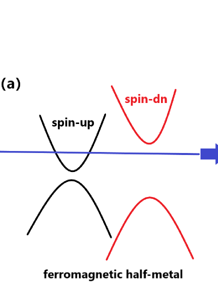
Fortunately, FV semiconductor with spontaneous spin and valley polarizations has been proposedq10 , which breaks time-reversal and space-inversion symmetry with perfect coupling of the valley with charge and spin. The FV semiconductors have been predicted in many 2D materialsq10 ; q11 ; q12 ; q13 ; q13-1 ; q19 ; gsd ; q14 ; q14-0 ; q14-0-1 ; q14-0-2 ; q14-0-3 ; q14-1 ; q17 ; q18 ; q14-2 ; q14-3 ; q14-4 ; q15 ; q16 , which can overcome these shortcomings of the extrinsic valley polarization materials. Recently, in analogy to half-metals in spintronics (see Figure 1), the concept of HVM has been proposedq10-1 . The conduction electrons of HVM are intrinsically 100% valley polarized and 100% spin polarized even when including spin-orbit coupling (SOC). The electron correlation effect or strain can induce the FV semiconductor to HVM transition in some special 2D materialsq14-0 ; q10-1 ; q10-2 ; a6 ; a7 , which is generally related to topological phase transitions. However, the HVM is just at one point, not a region of electron correlation strength or strain, which may be difficult to achieve in experiment.
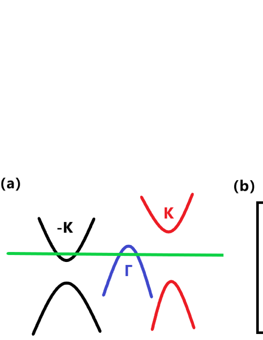
In this work, we propose a concept of QHVM, where electron and hole carriers simultaneously exist with only a type of carrier being valley polarized (see Figure 2). In QHVM, the Fermi level slightly touches the conduction band minima (CBM) and valence band maxima (VBM), and the Berry curvature in 2D Brillouin zone (BZ) only occurs around -K and K valleys with opposite signs and unequal magnitudes. Under an in-plane longitudinal electric field , the nonzero Berry curvature makes the carriers of -K valley obtain the general group velocity and the anomalous transverse velocity xd ; qqq :
| (1) |
where () is along the electric field direction (perpendicular to the electric field and out-of-plane directions). However, carriers of valley only obtain the general group velocity . The QHVM may be used to separate electron and hole carriers.
Recently, 2D family with a septuple-atomic-layer structure has been establisheda11 ; a12 with diverse properties from common semiconductor to FV semiconductor to topological insulator to Ising superconductor, and and of them have been achieved experimentally by the chemical vapor deposition method. Taking the monolayer as an example, the QHVM can be realized by electric filed. Within considered electric field range, the out-of-plane FM properties guarantee intrinsic spontaneous valley polarization in . The QHVM can be maintained in a certain range of electric field, and the related polarization properties can be effectively tuned. Our findings may be extended to other FV semiconductors, and the QHVM can be achieved by electric field tuning.
The rest of the paper is organized as follows. In the next section, we shall give our computational details and methods. In the next few sections, we shall present structure and stabilities, magnetic anisotropy (MA) and electronic structures and electric field effects on physical properties of monolayer. Finally, we shall give our discussion and conclusion.
II Computational detail
Within density-functional theory (DFT)1 , the spin-polarized first-principles calculations are performed by employing the projected augmented wave method, as implemented in Vienna ab initio simulation package (VASP)pv1 ; pv2 ; pv3 . We use the generalized gradient approximation of Perdew-Burke-Ernzerhof (PBE-GGA)pbe as exchange-correlation functional. The on-site Coulomb correlation of V atoms is considered by the GGA+ method in terms of the on-site Coulomb interaction of 3.0 eV, as widely used in V-based familyq14 ; q14-0-1 ; q14-0-2 ; q14-0-3 . The GGA+ adopts the rotationally invariant approach proposed by Dudarev et alu , in which only the effective () based on the difference between the on-site Coulomb interaction parameter and exchange parameters is meaningful.
To attain accurate results, we use the energy cut-off of 500 eV, total energy convergence criterion of eV and force convergence criteria of less than 0.0001 on each atom. A vacuum space of more than 20 is used to avoid the interactions between the neighboring slabs. A -centered 16 161 k-point meshs in the BZ are used for these calculations of structure optimization, electronic structures and elastic constants, and a 9161 Monkhorst-Pack k-point meshs for calculating FM/antiferromagnetic (AFM) energy with rectangle supercell, as shown in FIG.1 of electronic supplementary information (ESI) along with the first BZ. The SOC effect is explicitly included to investigate MCA and electronic properties of monolayer.
Through the direct supercell method, the interatomic force constants (IFCs) using GGA+ are calculated with the 551 supercell. Based on calculated harmonic IFCs, the phonon dispersions are obtained by using Phonopy codepv5 . The elastic stiffness tensor are carried out by using strain-stress relationship (SSR), and the 2D elastic coefficients have been renormalized by =, in which the is the length of unit cell along z direction. The Berry curvatures are directly calculated from wave functions based on Fukui’s methodbm by using VASPBERRY codebm1 ; bm2 .
III Structure and stability
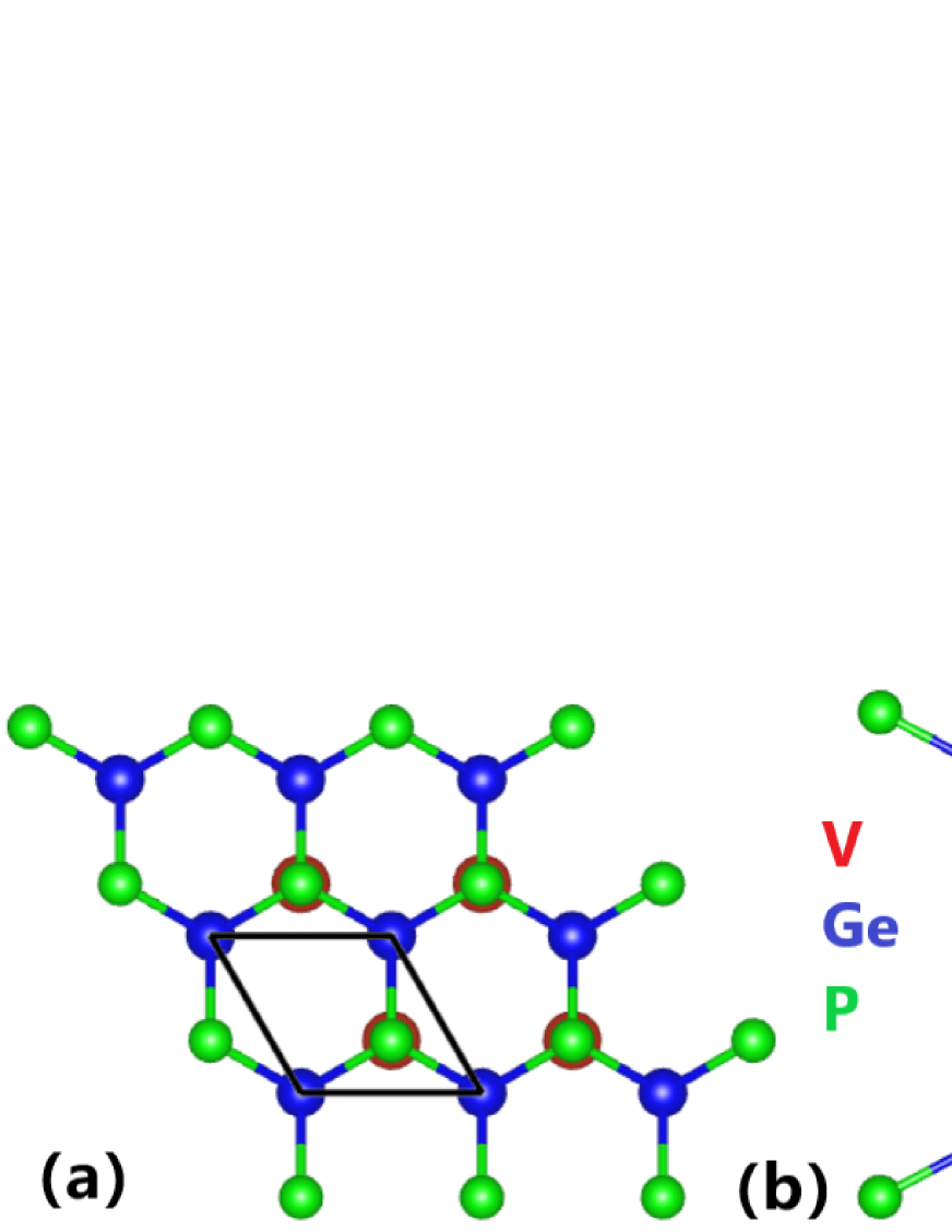
The crystal structures of monolayer are shown in Figure 3. Different from experimentally synthesized with phasea11 , the structure becomes favorable for a12 . Despite this difference, both and structures lack inversion symmetry with a space group of (No.187), which allows spontaneous valley polarization. The can be built by mirroring double layers of with respect to the vertical surface. This crystal includes seven covalently bonded atomic layers in the order of P-Ge-P-V-P-Ge-P along the axis. In other words, a -like layer is sandwiched between two slightly buckled honeycomb GeP layers. The optimized lattice constants of is 3.56 , which agrees well with with previous theoretical valuea12 . To obtain the magnetic ground state, the total energy difference between AFM and FM ordering by using rectangle supercell (FIG.1 of ESI) is calculated, and prefers FM state.
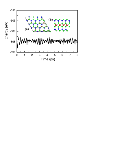
The dynamical stability of the monolayer is proved by analyzing the phonon spectra, as shown in Figure 3. There are eighteen optical and three acoustical phonon branches, corresponding to a total of twenty-one branches due to seven atoms per cell. It is found that all phonon frequencies are positive in 2D BZ, confirming the dynamical stability of at 0 K. Therefore, can exist as a free-standing monolayer. From the application point of view, the mechanical stability of is checked by elastic constants . Due to hexagonal symmetry, the has two independent elastic constants of and , and the calculated values are =182.68 and =51.16 . These of satisfy the Born criteria of mechanical stability ( and )ela , confirming its mechanical stability. The Ab initio molecular dynamics (AIMD) simulations are performed to assess the thermal stability of the monolayer at room temperature. Figure 4 shows the free energy as a function of the simulation time, along with the snapshots of the geometric structure at the end of AIMD simulation at 300 K. The free energy is fluctuated around the equilibrium values without any sudden changes, and the small distortions in the final configuration are observed. This confirms the thermodynamical stability of at room temperature, suggesting the possible room temperature applicability.
IV magnetic anisotropy and electronic structures
The magnetization of can affect its symmetry. For out-of-plane FM state, all possible vertical mirror symmetry is broken, but the horizontal mirror symmetry is preserved, allowing the spontaneous valley polarizationq14-0 ; q10-1 ; q10-2 ; a6 ; a7 . The MAE can be used to decide the orientation of magnetization of . The negative/positive MAE means an easy axis along the in-plane/out-of-plane direction. The MAE mainly includes MCA energy and MSA energy (). The SOC can produce a link between the crystalline structure and the direction of the magnetic moments, giving rise to . Based on GGA++SOC calculations, the can be obtained by , where and mean that spins lie in the plane and out-of-plane. Firstly, a collinear self-consistent calculation is performed to obtain the convergent charge density without SOC . Secondly, the convergent charge density is used to carry out noncollinear non-self-consistent calculation of two different magnetization directions (in-plane and out-of-plane) within SOC. The is due to the anisotropic dipole-dipole (D-D) interactiona1-7 ; a7-1 :
| (2) |
where the represent the local magnetic moments of V atoms, and vectors connects the sites and .
For a collinear FM monolayer, the Equation 2 for in-plane case can be expressed as:
| (3) |
where is the angle between the and . For out-of-plane situation, the Equation 2 can further be simplified as:
| (4) |
The ()can be written as :
| (5) |
It is clearly seen that the crystal structure and local magnetic moment decide . Generally, the MSA tends to make spins directed parallel to the monolayer.
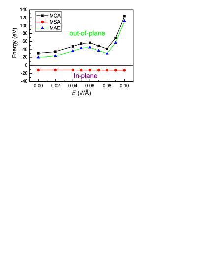
For V-based , has important effects on their magnetization directiongsd ; a7-1-1 ; a7-1-2 . For monolayer, an out-of-plane ferromagnet is predicted, when only is consideredq14 . However, the will prefer in-plane case with including gsd . Calculated results show that is a FV semiconductor for out-of-plane case using GGA+ (= 3 eV), and it will become a common magnetic semiconductor for in-plane situationgsd ; q14 . So, the is considered to decide magnetization direction of . Calculated results show that the MAE is 19 with and being 31 and -12 , and the positive MAE means that the easy magnetization axis of is out-of-plane.
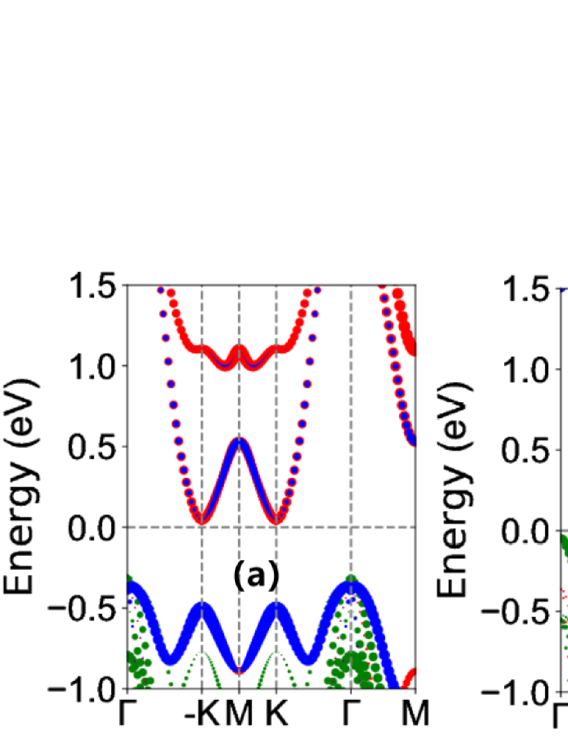
The spin-polarized band structures of monolayer by using both GGA+ and GGA++SOC are calculated. In a trigonal prismatic crystal field environment, the V- orbitals split into orbital, + and + orbitals, and these orbital characters energy band structures without SOC and with SOC are plotted in Figure 5. Based on Figure 5 (a) and (b), a distinct spin splitting can be observed due to the exchange interaction. It is found that is an indirect band gap semiconductor of 0.091 eV, and its VBM and CBM are provided by the spin-dn and spin-up. The energies of -K and K valleys for both conduction and valence bands are degenerate, and no spontaneous valley polarization is observed.
The spontaneous valley polarization is induced by SOC. Calculated results show observable valley splitting between -K and K valleys in the conduction bands, and neglectful valley splitting in the valence bands. This difference can be explained by the distribution of V- orbitals. According to Figure 5, it is found that + orbitals dominate -K and K valleys of conduction bands, while the ones of valence bands are mainly from orbitals. A simple perturbation theory can be used to further elucidate the essence of the valley polarization with SOC Hamiltonian of out-of-plane magnetization q18 ; v2 :
| (6) |
in which and are the orbital angular moment along direction and coupling strength. In light of the orbitals’ contribution to -K and K valleys and their wave vector symmetry, the basis functions are chosen as:
| (7) |
| (8) |
where the subscript , and represent conduction bands, valence bands and valley index (). The energy levels at -K and K valleys are then defined as:
| (9) |
According to the distribution of V- orbitals, the valley splitting in the bottom conduction and top valence bands are given byq18 ; v2 :
| (10) |
| (11) |
The perturbation theory results are in excellent consistency with the first-principle calculations.
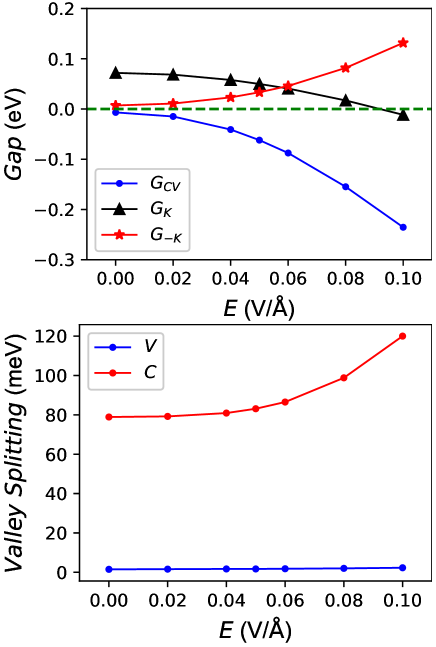
According to Figure 5 (c), the becomes a metal with a negative gap () of -7 meV, when the SOC is included. The Fermi level slightly touches the CBM (-K valley) and VBM ( valley), but has no contact with K valley. Therefore, monolayer is a QHVM. To describe properties of QHVM, two other gaps are defined. One is the Fermi level minus the energy of -K valley in the conduction bands (), which can describe concentration of electron carriers. Another is the energy of K valley in the conduction bands minus the Fermi level (), which describes how easy the carriers of -K valley jump to K valley. The plus equals to valley splitting in the conduction bands. For , the is only about 7 meV, so it needs to be regulated through the external field, for example electric field.
V electric field effects
Electric field can induce a semiconductor to metal transition in bilayer and apl . Moreover, the increasing electric field can result in a transition of MA from in-plane to out-of-plane in jmcc . In view of these facts, electric field may tune physical properties of QHVM in . Firstly, we confirm the magnetic ground state under the electric field by the energy differences (per formula unit) between AFM and FM ordering, which are plotted in FIG.2 of ESI. Within considered range, the FM ordering is always ground state. The MAE along with and as a function of are plotted in Figure 6. It is found that the is positive within considered range, which firstly increases, then decreases, and then increases with increasing . The can be obtained by Equation 5. FIG.3 of ESI shows the local magnetic moment of V atom () as a function of . It is found that the has very little effects on within considered range, and the change is only 0.021 , which leads to the small change of from -11.58 to -12.03 . Finally, we calculate the MAE by =+. It is clearly seen that and have the same trend with respect to . In considered range, is always positive, implying that possesses out-of-plane MA. This confirms spontaneous valley polarization in within considered range.
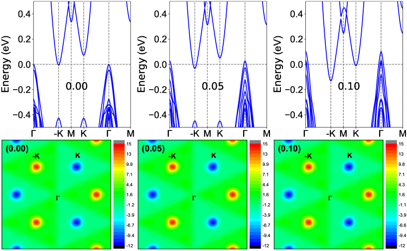
The energy band structures and Berry curvature distribution of under electric field are investigated, and some representative ones are plotted in Figure 7. The evolutions of related gap (, and ) and valley splitting for both valence and condition bands as a function of are shown in Figure 8. With increasing , the increases, which means that concentration of electron carriers increases. However, the decreases, which means that the carriers of -K valley more easily jump to K valley. When 0.09 , the Fermi energy level simultaneously touches the -K and K valleys, and the QHVM will disappear. It is found that the increasing can enhance valley splitting of conduction bands. So, the electric field can effectively tune physical properties of QHVM in . By applying an in-plane longitudinal in , anomalous velocity of Bloch electrons at -K valley is related with Berry curvature (see Figure 7):xd ; qqq . The Berry curvature of -K valley forces the electron carriers to accumulate on one side of the sample, and the hole carriers of valley move in a straight line. When an out-of-plane electric fields is applied, the carrier concentration can be effectively tuned.
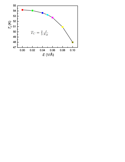
To estimate Curie temperature of , it can be simply considered as a Ising spin system. The transition temperature can be expressed as by using the mean-field approximations (MFA)re8 , where and are the nearest-neighboring exchange parameter and Boltzmann constant, respectively. The can be obtained from the energy difference between AFM () and FM () orderings. According to the FM and AFM configurations, the and can be written as:
| (12) |
| (13) |
in which is the total energy of systems without magnetic coupling. The corresponding can be attained:
| (14) |
The vs is plotted in Figure 9. Within range, the predicted is larger than 48 K.
VI Discussion and Conclusion
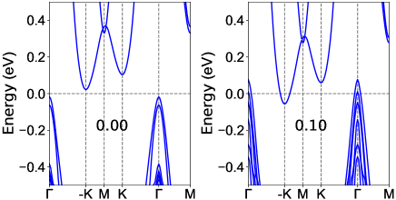
For a given material, the correlation strength should be determined from future experiment. Here, the = 4 eV is also used to investigate related properties of to confirm that the QHVM can indeed be achieved by electric field tuning. FIG.4 of ESI shows that the FM ordering is ground state, when 0.19 . The , and along with the local magnetic moment of V atom () as a function of are plotted in FIG.5 and FIG.6 of ESI. When 0.19 , the positive implies that has out-of-plane MA. The evolutions of related gap (, and ) as a function of are shown in FIG.7 of ESI. The representative energy band structures at 0.00 and 0.10 are plotted in Figure 10. Without electric field, is a FV semiconductor with an indirect band gap of 0.040 eV. The increasing can induce FV semiconductor to QHVM transition with critical of about 0.05 . However, when 0.15 , the QHVM will disappear. For example =0.10 , the is a QHVM with , and being -0.133 eV, 0.056 eV and 0.060 eV. When correlation strength is in the reasonable range of 3 eV to 4 eV, the can be tuned into QHVM by electric field.
In summary, we have proposed the concept of QHVM, which may be realized in monolayer with dynamical, mechanical and thermal stabilities. The electric field can be used tune the related physical properties of QHVM in . For a certain electric field region, QHVM properties can be maintained, and the carrier concentration of -K valley can be effectively tuned. When in-plane and out-of-plane electric fields are applied, the electron carriers of -K valley transversely drift and eventually accumulate on one edge of the sample, while the hole carriers of valley longitudinally move along the in-plane electric field direction. Our findings can inspire more works to search for QHVM.
Conflicts of interest
There are no conflicts to declare.
Acknowledgements.
This work is supported by Natural Science Basis Research Plan in Shaanxi Province of China (2021JM-456). We are grateful to Shanxi Supercomputing Center of China, and the calculations were performed on TianHe-2.References
- (1) J. R. Schaibley, H. Yu, G. Clark, P. Rivera, J. S. Ross, K. L. Seyler, W. Yao and X. Xu, Nat. Rev. Mater. 1, 16055 (2016).
- (2) L. J. Sham, S. J. Allen, A. Kamgar, and D. C. Tsui, Phys. Rev. Lett. 40, 472 (1978).
- (3) S. A. Wolf, D. D. Awschalom, R. A. Buhrman, J. M. Daughton, S. von Molnr, M. L. Roukes, A. Y. Chtchelkanova, and D. M. Treger, Science 294, 1488 (2001).
- (4) A. Srivastava, M. Sidler, A. V. Allain, D. S. Lembke, A. Kis, and A. Imamoglu, Nat. Phys. 11, 141 (2015).
- (5) K. F. Mak, K. He, J. Shan, and T. F. Heinz, Nat. Nanotechnol. 7, 494 (2012).
- (6) H. Zeng, J. Dai, W. Yao, D. Xiao, and X. Cui, Nat. Nanotechnol. 7, 490 (2012).
- (7) 8 H. Zeng, J. Dai, W. Yao, D. Xiao and X. Cui, Nat. Nanotechnol. 7, 490 (2012).
- (8) M. Zeng, Y. Xiao, J. Liu, K. Yang and L. Fu, Chem. Rev. 118, 6236 (2018).
- (9) C. Zhao, T. Norden, P. Zhang, P. Zhao, Y. Cheng, F. Sun, J. P. Parry, P. Taheri, J. Wang, Y. Yang, T. Scrace, K. Kang, S. Yang, G. Miao, R. Sabirianov, G. Kioseoglou, W. Huang, A. Petrou and H. Zeng, Nat. Nanotechnol. 12, 757 (2017).
- (10) D. MacNeill, C. Heikes, K. F. Mak, Z. Anderson, A. Kormnyos, V. Zlyomi, J. Park and D. C. Ralph, Phys. Rev. Lett. 114, 037401 (2015).
- (11) W. Y. Tong, S. J. Gong, X. Wan, and C. G. Duan, Nat. Commun. 7, 13612 (2016).
- (12) Y. B. Liu, T. Zhang, K. Y. Dou, W. H. Du, R. Peng, Y. Dai, B. B. Huang, and Y. D. Ma, J. Phys. Chem. Lett. 12, 8341 (2021).
- (13) Z. Song, X. Sun, J. Zheng, F. Pan, Y. Hou, M.-H. Yung, J. Yang, and J. Lu, Nanoscale 10, 13986 (2018).
- (14) J. Zhou, Y. P. Feng, and L. Shen, Phys. Rev. B 102, 180407(R) (2020).
- (15) P. Zhao, Y. Ma, C. Lei, H. Wang, B. Huang, and Y. Dai, Appl. Phys. Lett. 115, 261605 (2019).
- (16) S. D. Guo, J. X. Zhu, W. Q. Mu and B. G. Liu, Phys. Rev. B 104, 224428 (2021).
- (17) S. D. Guo, Y. L. Tao, K. Cheng, B. Wang and Y. S. Ang, J. Phys.: Condens. Matter (2022). https://doi.org/10.1088/1361-648X/ac9c3d
- (18) X. Y. Feng, X. L. Xu, Z. L. He, R. Peng, Y. Dai, B. B. Huang and Y. D. Ma, Phys. Rev. B 104, 075421 (2021).
- (19) S. Li, Q. Q. Wang, C. M. Zhang, P. Guo and S. A. Yang, Phys. Rev. B 104, 085149 (2021).
- (20) Q. R. Cui, Y. M. Zhu, J. H. Liang, P. Cui and H. X. Yang, Phys. Rev. B 103, 085421 (2021).
- (21) Y. L. Wang and Y. Ding, Appl. Phys. Lett. 119, 193101 (2021).
- (22) X. Zhou, R. Zhang, Z. Zhang, W. Feng, Y. Mokrousov and Y. Yao, npj Comput. Mater. 7, 160 (2021).
- (23) H. X. Cheng, J. Zhou, W. Ji, Y. N. Zhang and Y. P. Feng, Phys. Rev. B 103, 125121 (2021).
- (24) W. Du, Y. Ma, R. Peng, H. Wang, B. Huang, and Y. Dai, J. Mater. Chem. C 8, 13220 (2020).
- (25) R. Li, J. W. Jiang, W. B. Mi and H. L. Bai, Nanoscale 13, 14807 (2021).
- (26) K. Sheng, Q. Chen, H. K. Yuan and Z. Y. Wang, Phys. Rev. B 105, 075304 (2022).
- (27) P. Jiang, L. L. Kang, Y. L. Li, X. H. Zheng, Z. Zeng and S. Sanvito, Phys. Rev. B 104, 035430 (2021).
- (28) K. Sheng, H. K. Yuan and B. K. Zhang, Nanoscale (2022).DOI: 10.1039/d2nr03860a
- (29) Y. Zang, Y. Ma, R. Peng, H. Wang, B. Huang, and Y. Dai, Nano Res. 14, 834 (2021).
- (30) R. Peng, Y. Ma, X. Xu, Z. He, B. Huang, and Y. Dai, Phys. Rev. B 102, 035412 (2020).
- (31) H. Hu, W. Y. Tong, Y. H. Shen, X. Wan, and C. G. Duan, npj Comput. Mater. 6, 129 (2020).
- (32) K. Sheng, B. K. Zhang, H. K. Yuan and Z. Y. Wang, Phys. Rev. B 105, 195312 (2022).
- (33) S. D. Guo, J. X. Zhu, M. Y. Yin and B. G. Liu, Phys. Rev. B 105, 104416 (2022).
- (34) S. D. Guo, W. Q. Mu and B. G. Liu, 2D Mater. 9, 035011 (2022).
- (35) X. Xu, W. Yao, D. Xiao and T. F. Heinz, Nat. Phys. 10, 343 (2014).
- (36) D. Xiao, M. C. Chang, and Q. Niu, Rev. Mod. Phys. 82, 1959 (2010).
- (37) Y. L. Hong, Z. B. Liu, L. Wang T. Y. Zhou, W. Ma, C. Xu, S. Feng, L. Chen, M. L. Chen, D. M. Sun, X. Q. Chen, H. M. Cheng and W. C. Ren, Science 369, 670 (2020).
- (38) L. Wang, Y. Shi, M. Liu, A. Zhang, Y.-L. Hong, R. Li, Q. Gao, M. Chen, W. Ren, H.-M. Cheng, Y. Li, and X.- Q. Chen, Nat. Commun. 12, 2361 (2021).
- (39) P. Hohenberg and W. Kohn, Phys. Rev. 136, B864 (1964); W. Kohn and L. J. Sham, Phys. Rev. 140, A1133 (1965).
- (40) G. Kresse, J. Non-Cryst. Solids 193, 222 (1995).
- (41) G. Kresse and J. Furthmller, Comput. Mater. Sci. 6, 15 (1996).
- (42) G. Kresse and D. Joubert, Phys. Rev. B 59, 1758 (1999).
- (43) J. P. Perdew, K. Burke and M. Ernzerhof, Phys. Rev. Lett. 77, 3865 (1996).
- (44) S. L. Dudarev, G. A. Botton, S. Y. Savrasov, C. J. Humphreys and A. P. Sutton, Phys. Rev. B 57, 1505 (1998).
- (45) A. Togo, F. Oba, and I. Tanaka, Phys. Rev. B 78, 134106 (2008).
- (46) T. Fukui, Y. Hatsugai and H. Suzuki, J. Phys. Soc. Japan. 74, 1674 (2005).
- (47) H. J. Kim, https://github.com/Infant83/VASPBERRY, (2018).
- (48) H. J. Kim, C. Li, J. Feng, J.-H. Cho, and Z. Zhang, Phys. Rev. B 93, 041404(R) (2016).
- (49) E. Cadelano and L. Colombo, Phys. Rev. B 85, 245434 (2012).
- (50) X. B. Lu, R. X. Fei, L. H. Zhu and L. Yang, Nat. Commun. 11, 4724 (2020).
- (51) K. Yang, G. Y. Wang, L. Liu , D. Lu and H. Wu, Phys. Rev. B 104, 144416 (2021).
- (52) S. D. Guo, W.-Q. Mu, J.-H. Wang, Y.-X. Yang, B. Wang and Y.-S. Ang, Phys. Rev. B 106, 064416 (2022).
- (53) D. Dey, A. Ray and L. P. Yu, Phys. Rev. Materials 6, L061002 (2022).
- (54) P. Zhao, Y. Dai, H. Wang, B. B. Huang and Y. D. Ma, ChemPhysMater, 1, 56 (2022).
- (55) Q. Y. Wu, L. M. Cao, Y. S. Ang and L. K. Ang, Appl. Phys. Lett. 118, 113102 (2021).
- (56) S. D. Guo, X. S. Guo, G. Z. Wang, K. Cheng and Y. S. Ang, J. Mater. Chem. C (2022). https://doi.org/10.1039/D2TC03293G
- (57) L. Ke, B. N. Harmon, and M. J. Kramer, Physical Review B 95, 104427 (2017).