Phase-Space Ab-Initio Direct and Reverse Ballistic-Electron Emission Spectroscopy: Schottky Barriers Determination for Au/Ge(100)
Abstract
We develop a phase-space ab-initio formalism to compute Ballistic Electron Emission Spectroscopy current-voltage I(V)’s in a metal-semiconductor interface. We consider injection of electrons into the conduction band for direct bias () and injection of holes into the valence band or injection of secondary Auger electrons into the conduction band for reverse bias (). Here, an ab-initio description of the semiconductor inversion layer (spanning hundreds of Angstroms) is needed. Such formalism is helpful to get parameter-free best-fit values for the Schottky barrier, a key technological characteristic for metal-semiconductor rectifying interfaces. We have applied the theory to characterize the Au/Ge(001) interface; a double barrier is found for electrons injected into the conduction band – either directly or created by the Auger process – while only a single barrier has been identified for holes injected into the valence band.
I Introduction
An accurate value for the metal-semiconductor Schottky barrier () is of paramount importance to characterize the rectifying performance of solid-state semiconductor devices Sze and Kwok (2006). Furthermore, the increasing trend in miniaturization highlights the need for techniques that can provide values for related to the microscopic active Schottky region of interest in each case. Ballistic Electron Emission Microscopy (BEEM) is the foremost technique to obtain precise microscopic values for the Schottky barrier Bell and Kaiser (1988); Bannani et al. (2008), and to study the influence of interface coupling on the electronic properties Cook et al. (2015); Wong et al. (2020), but also to study magnetic materials, organic layers, electronic band structure and hot-carrier scattering Bell (2016) and molecular semiconductors Zhou et al. (2021).
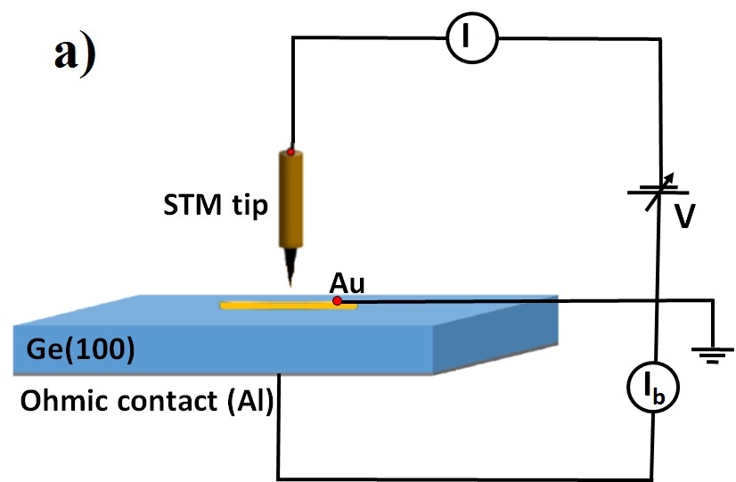
BEEM is a scanning tunnelling microscopy (STM)-based technique that can directly measure the barrier height at the metal/semiconductor interface with spatial nanoscale resolution Yi et al. (2009); Bobisch et al. (2009); Bobisch and Möller (2012); Qin et al. (2012); Parui et al. (2013); Nolting et al. (2016). The STM tip at bias injects ballistic electrons into a thin metal overlayer at constant tunnelling current (Figure 1-a). When the electron’s kinetic energy of the injected electrons is higher than the local Schottky barrier formed between the metal and the semiconductor, the electrons can overcome the local barrier and a current is transmitted across the sample and collected through the backside Ohmic contact (Figure 1-a) Wu et al. (2013); Janardhanam et al. (2019). Accurate Ballistic Electron Emission Spectroscopy (BEES) determination for the Schottky threshold relies on a best-fit where experimental measurements are compared with a theoretical model where currently the state-of-the-art standard claims accuracies between 10 and 30 meV Gerbi et al. (2020); Rogers et al. (2021). Such a procedure has been successfully used before in other fields, like structural work related to diffraction techniques, and requires the use of theory as accurate as possible and free of adjustable parameters to avoid spurious correlations in the determination of the value of . A serious description of BEES must consider four basic steps: (i) tunnelling from the STM tip to the metal base, (ii) transport through the metal base, (iii) transmission and reflection at the interface and (iv) injection into the semiconductor conduction (, electrons) or valence (, holes) bands. The Keldysh non-equilibrium Greens functions formalism developed in Claveau et al. (2017) performs such tasks. Such theory has been complemented with an ab-initio LCAO procedure Lewis et al. (2011) to build the relevant Hamiltonians making the calculations free from a particular parametrization and more general Gerbi et al. (2018). Further, the whole procedure has been used to analyse experiments on Ge/Au and Ge/Pt for the injection of electrons on the semiconductor conduction band (, direct BEES) Gerbi et al. (2020).
Such analysis is incomplete if the injection of holes in the semiconductor valence band is not included (i.e. reverse BEES, ) Balsano et al. (2013); Filatov et al. (2014, 2018). In this paper, we extend our previous work to such a new domain. The analysis of reverse experimental I(V) curves shows the necessity to include two new processes that were neglected for :
-
1.
The energy losses by quasi-elastic electron-phonon interaction in the depletion layer and,
-
2.
The formation of electron-hole pairs due to secondary Auger-like inelastic electron-electron interaction.
The value of the effective phase-space volume, , includes an ab-initio calculation for each pair of metal-semiconductor interfaces that has to be determined independently for the conduction and valence band. In addition, we derive the modification of because of the aforementioned two inelastic processes. is approximately increased by because of phonons and by because of Auger electrons. Finally, attenuation due to inelastic electron-electron scattering and multiple reflections in the metal base has been thoroughly analyzed in the literature and are necessary ingredients to a complete theoretical description Reuter et al. (2000); Parui et al. (2013).
In summarizing, the formalism presented here provides a simple expression to compute I(V)’s for the whole domain of voltages within the phase-space approach. It returns accurate parameter-free values of Schottky barriers for positive and negative bias, allowing the characterization of Schottky barriers with respect to both the conduction and valence bands. Therefore, we have generalized the previous phenomenological ideas by Kaiser and Bell and Ludeke Bell et al. (1991); Ludeke (1993a), providing an improved level of analysis for experimental data. Finally, as a by-product of the work done to check and illustrate our theory, we study germanium as a promising material for high performance devices Hu et al. (2011); Scappucci et al. (2013) and we obtain relevant values for the technologically important Schottky interface Au/Ge by comparing with experiments.
II Experimental
BEES IVs have been taken on Au/Ge(100) with Ge substrates at three different doping levels (n-type, Sb-doped, MTI Corporation). Samples were cut into pieces of 10 mm 5 mm sizes and cleaned with acetone and 2-propanol. In order to remove the native oxide, we immersed the samples in hot water at C, Furthermore, we immediately dried it with nitrogen. We then dipped it in an HF solution at 3% to remove the residual \ceGeOx not soluble in hot water and to obtain a hydrogen-terminated Ge(100) surface. The cleaned Ge pieces were loaded within a few minutes into the UHV deposition chamber for the Au contact fabrication, obtained by Physical Vapor Deposition (PVD) from a tungsten coil through a shadow mask (vacuum pressure torr, the deposition rate was nm min-1). A representative set of five averaged spectra was considered. Spectra 1 and 2 correspond to the high doping regime n-Ge case, i.e. to -cm. The three other spectra correspond to different n-Ge doping regimes: (i) to -cm for spectrum 3 ( cm-3, high-doping regime), (ii) - -cm for spectrum 4 ( cm-3, medium-doping regime) and (iii), - -cm for spectrum 5 ( cm-3, low-doping regime). The nominal thicknesses of the metal contacts was in the range to nm for the low doping level samples and it was intentionally kept smaller, to nm, for the high doping level. As discussed below, the doping level and the metal contact thickness are critical parameters that control the detection of ballistic holes or the generation of secondary Auger-like electrons in BEES reverse bias voltage. The contact area was 2.4 mm2 for all devices. The Ohmic back contact was fabricated by depositing a thick Al film by pulsed laser deposition at room temperature from a high-purity target Gerbi et al. (2014); Buzio et al. (2018). Immediately after contact with the active area of the diode was established we have transferred the sample to the UHM LT-STM chamber for BEEM measurements. We have performed the experiments using a modified commercial STM equipped with an additional low-noise variable-gain current amplifier Gerbi et al. (2018); Buzio et al. (2020). Data were taken in the dark and at K to improve the signal-to-noise ratio. For the acquisition of each BEEM spectrum, the tip voltage was ramped under feedback control, keeping the tunnelling current constant. Noise current fluctuations in individual raw spectra amounted to fA rms. We find that such a low noise level is required for the accurate determination of Schottky barriers by comparing theory and experiment.
III Results and discussion
III.1 BEES analysis from the phenomenological Bell-Kaiser model
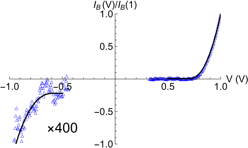
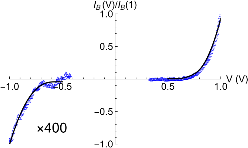
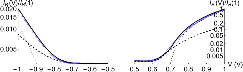
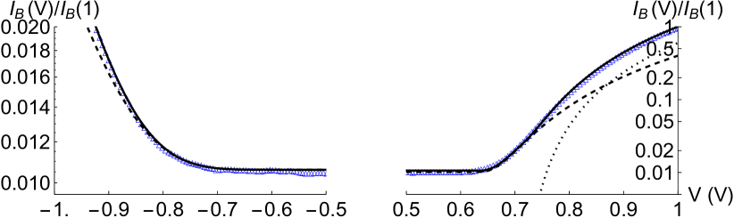
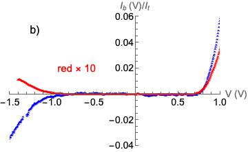
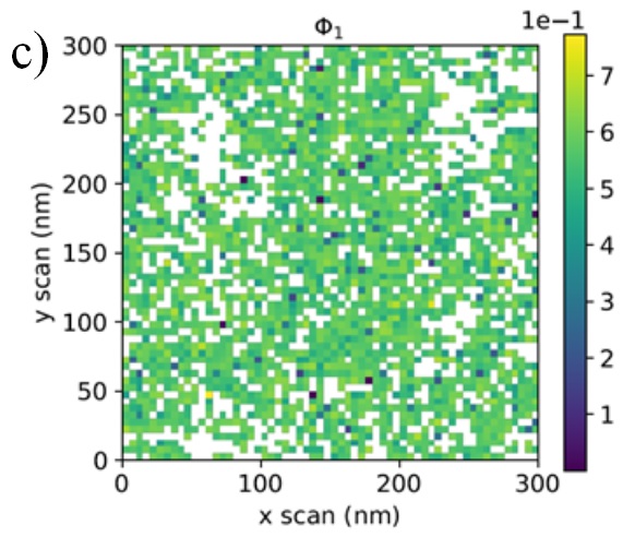
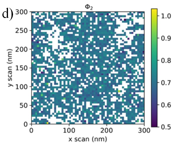
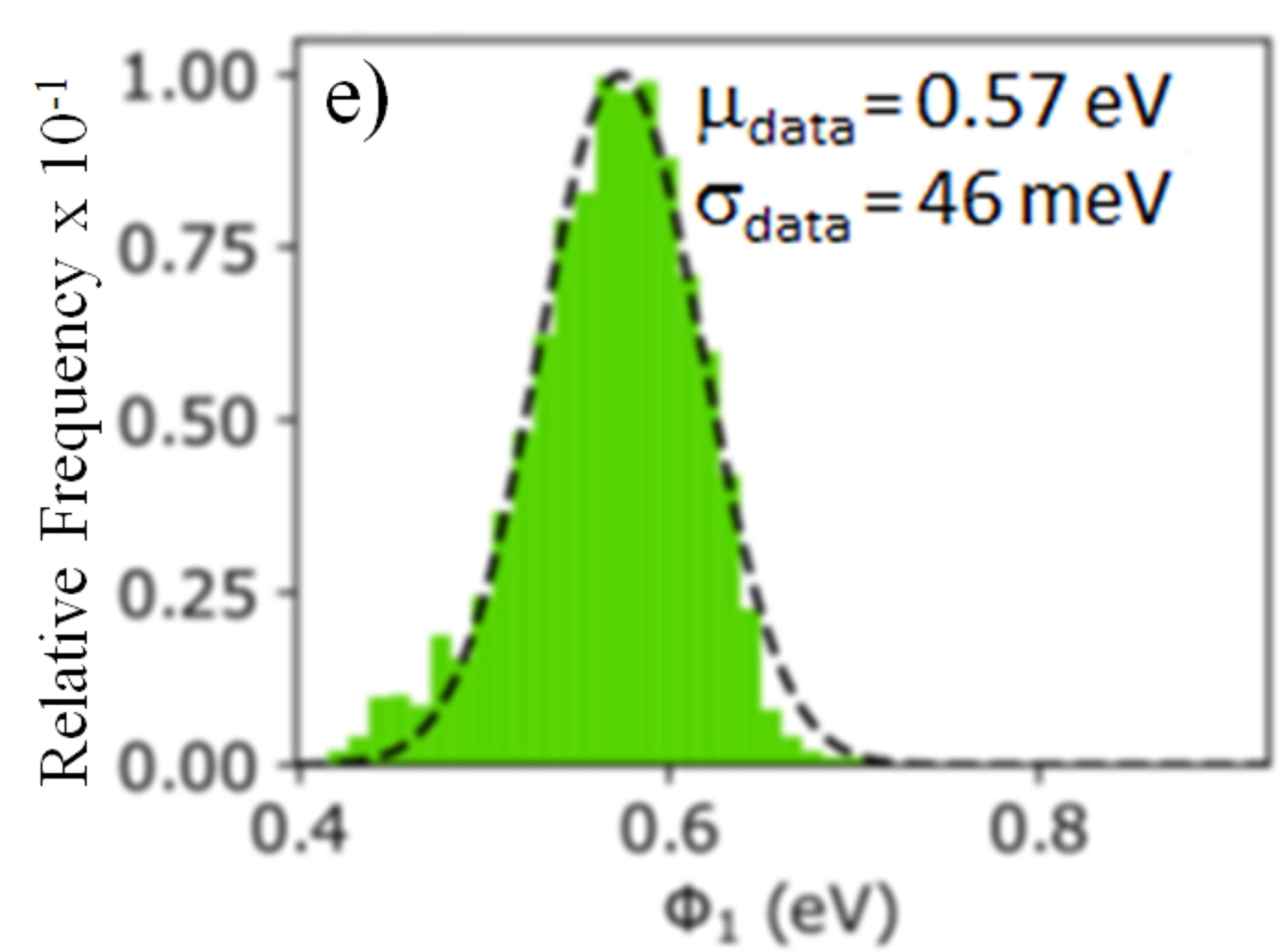
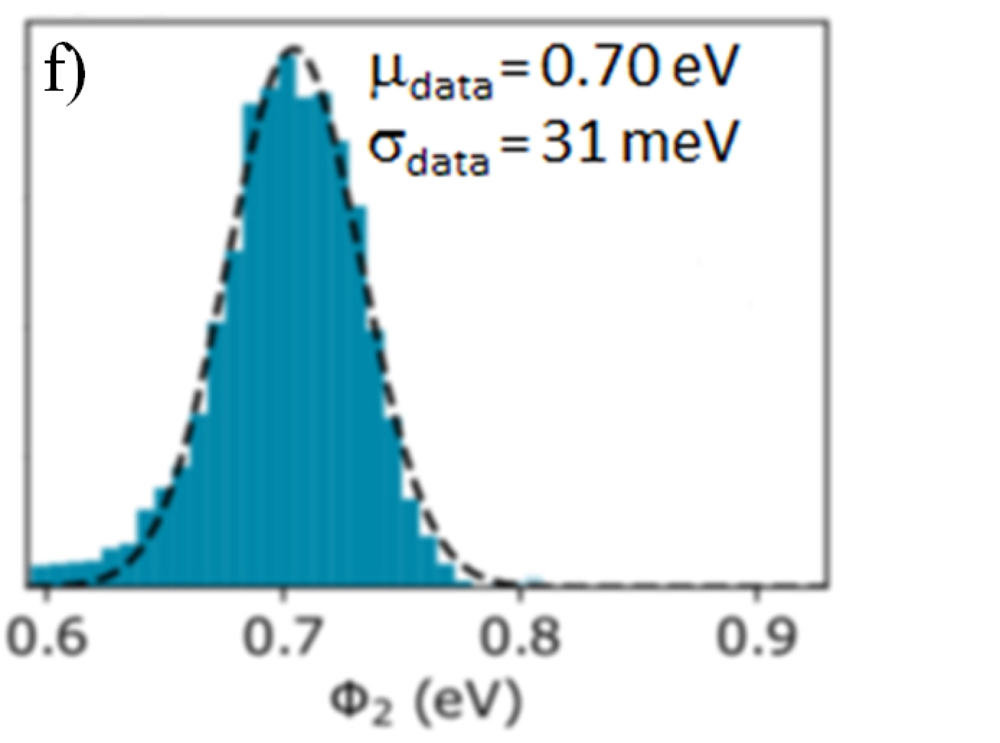
The local Schottky barrier, , is obtained from a best-fit analysis of the variation of the collector current in a small interval near the onset, versus , both for the direct BEEM (DBEEM) and for the reverse BEEM (RBEEM). In Figure 1-b, we show representative spectra acquired on two different devices, where the hole injection (blue curve, high doping regime) or Auger-like injection (red curve, low doping regime) are the dominant mechanisms in reverse polarization ( and , respectively). Briefly, we have observed hole injection only for (i) diodes prepared on high doping substrates and, (ii) at the edges of the active region of the diode, where the metal thickness is reduced just to a few nm. Under such specific conditions we have observed the inversion of the current () in the RBEEM spectra for about 25% of the cases. However, we were unable to spatially resolve the phenomenon. In all other situations, the Auger-like injection mechanism () was dominant in RBEEM spectra. According to previous phenomenological ideas by Kaiser and Bell, and Ludeke Bell and Kaiser (1988); Ludeke (1993b), in the case of Auger-like injection one can get quantitative information on the local Schottky barrier height by fitting an ensemble of about raw spectra acquired on a grid of points (Figures 1-c,d), using a double barrier Bell-Kaiser model with n=4 for RBEEM, . We estimate from histogram analysis a double barrier distribution centred at eV and eV (Figures 1-e,f), with spatially resolved statistics. These values are slightly different from the full theoretical calculation we present below because they are obtained by comparing against a phenomenological model which uses a mere approximation to the actual volume in phase-space available for injection of carriers and, it does not include the effect of temperature. Nevertheless, such model provides a quick way to analyze data and as we shall see, it is remarkably close to a more complete theoretical description.
III.2 Phase-Space formalism
We continue our phase-space ballistic-electron formalism for the direct bias () injection of electrons from the tip to the semiconductor band Gerbi et al. (2020) to the inverse polarization domain (). First, we obtain the effective phase-space volume near the Schottky onset for injecting into the semiconductor electrons (conduction band) or holes (valence band). These values are obtained from an ab-initio Keldysh’s Greens functions calculation. They are represented by a characteristic value of in Eq. (1), which only depends on the particular metal-semiconductor interface pair.
Inelastic processes merely attenuate the intensity of electrons injected into the conduction band (), which can be easily accounted for by introducing an exponential factor that depends on a characteristic mean free path for electrons, . The scenario for reverse bias, however, becomes more involved. First, the current of holes ( for ) can only be detected for highly doped samples ( cm-3). Indeed, the current of holes injected into the semiconductor valence band under reverse bias voltage is heavily attenuated w.r.t. the current of ballistic electrons for positive voltage, as demonstrated by taking the ratio of experimental intensities (e.g., cf. Figs 7 and 8). As we shall see, quasi-elastic phonon-hole interaction inside the inversion layer is mainly responsible for such behaviour. Second, the appearance of Auger-like electron-hole pairs excitations create a secondary current of electrons injecting into the conduction band () that eventually dominate the negative current of holes injecting into the valence band (e.g., cf. Figs 9, 10, and 11). As explained in A.2 and A.3, we take into account those effects by modifying the effective phase-space volume by adding a power-law term in Equation 1. For the interaction of ballistic holes with phonons, we obtain , while for the generation of secondary Auger electrons, we get . Therefore, the phase-space formula for the reverse BEES can again be written in a simple closed-form as,
| (1) |
where, is the value for the onset (Schottky barrier) to be sought (eV), is the tip voltage measured w.r.t to the onset (eV), is the absolute temperature (K), is a proportionality constant used to normalise the current, is the effective dimension of the equivalent ballistic phase space determined from ab-initio calculations, determines a power-law approximation to the probability of scattering with other quasiparticles, e.g. phonons or secondary Auger electrons, as discussed in detail in A.1 and A.3, is a baseline current below the onset due to noise fluctuations, and and Li are the incomplete Euler Gamma function and the Jonquière’s function respectively Weisstein (2018).
One advantage of subsuming an accurate but complex ab-initio calculation in a simple analytical formula such as Eq. 1 is the flexibility to include new physical effects. The importance of interfaces in performing devices cannot be overstated, and their continuing influence is foreseen in new challenging domains like spintronics Hervé et al. (2013a, b) and devices based on molecular semiconductors, in particular the determination of the metal/molecule energy and the electronic transport gap Zhou et al. (2021). In that direction, the next step to developing Eq. 1 will be to study spin-polarized effects.
III.3 BEES analysis from phase-space formalism
We have analysed results for five different ensemble-averaged spectra, acquired at specific spots of the Schottky metal pad. Spectra 1 and 2 correspond to the high doping case ( to -cm) and to the thin regions nearby the edge of the pad, where electron-electron inelastic effects for reverse injection are negligible. Therefore, the injection of holes in the valence band dominates the reverse current. On the other hand, spectra 3, 4 and 5 correspond to the central regions of the metal pad and show strong Auger-like strong re-injection of electrons in the semiconductor conduction band under reverse polarisation.
III.3.1 Injection of electrons in the semiconductor conduction band (direct polarisation)
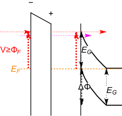
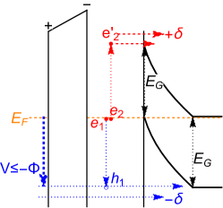
First, let us consider the injection of electrons from the tip into empty states in the semiconductor conduction band (cf. Figure 2, top-left diagram, for ). As a reasonable approximation, we neglect tunnelling through the space-charge layer owing to its extension. Thermal excitation of carriers is described by the Fermi-Dirac distribution, which is embedded in our analytical result in Eq. (1). Therefore, for direct bias (), we are only concerned with the injection of electrons in the available empty states in the conduction band. In Section III.3.3, we shall consider the injection of secondary Auger electrons, also into the conduction band, making a positive current for negative bias polarization.
We apply the ab-initio approach developed in Gerbi et al. (2018, 2020); for Au/Ge we have , resulting in the values in Table 1 (for comparison, in the Pt/Ge we get and for the Au/Si interface we have determined ). The main finding is the values for two onsets, at and eV. The second onset for spectra 3, 4 and 5 draws off about ten times more electrons than the first one, as judged by the ratio between intensities . On the other hand, for the spectra 1 and 2, the ratio goes up to 30 or 60. In a previous paper, we have extensively discussed the role of interfacial structural contributions to the origin of the double barrier Gerbi et al. (2020). Both ab-initio modelling and X-ray diffraction support the existence of two different atomic registries at the metal-semiconductor interface resulting in a shift in the Schottky barriers of eV. Such value is in good agreement with our experimental findings. Nonetheless, using our current BEES analysis only, we cannot confidently exclude electronic effects associated with different conduction band minima as suggested in Prietsch and Ludeke (1991).
The attenuation of currents of ballistic electrons is related to the thickness of the metal base layer. It can be estimated by considering the ratio of intensities between a thin and a thick sample. As an example, we take the red and blue curves in Figure 1-b ( and respectively) . We get for the ratio of experimental intensities , where the mean and the standard deviation have been estimated by considering the small interval eV around eV. This value can be reconciled with the following simple model: a theoretical mean free path in Au, Å, an estimated length difference between the thick and the thin samples of Å, a transmission factor at the metal-semiconductor interface of , and five multiple internal reflectionsReuter et al. (2000),
| (2) |
| S | |||
|---|---|---|---|
| 1 | 0.9995 | ||
| 2 | 0.9986 | ||
| 3 | 0.9996 | ||
| 4 | 0.9994 | ||
| 5 | 0.9999 | ||
| A |
III.3.2 Injection of holes in the semiconductor valence band (reverse polarisation)
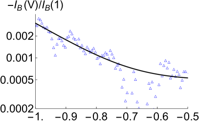
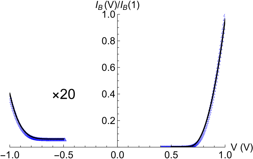
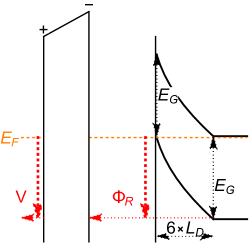
Second, we consider the injection of holes into the semiconductor valence band ( and ), demonstrated in spectra 1 and 2. As comented while discussing Equation 1, the reverse current of holes is weaker than the direct current of electrons. The main scattering mechanism responsible for such a strong attenuation is the quasi-elastic interaction with phonons in the inversion layer. The attenuation ratio can vary in a wide range depending on the characteristics of the sample, e.g. from in Figure 1-b (blue curve) to in Figures 7 and 8. Such sensitivity is related to the short mean free path for holes. We have computed in Section A.4.1 that for a doping of cm3 we have Å and a typical width for the inversion layer of Å. These values depend significantly on the amount of doping and, for a higher doping of cm3 the inversion layer becomes merely Å. Therefore, the need to include the attenuation due to phonons to describe ballistic currents of holes, as explained in the discussion of Equation 1. The following stringent conditions must be attained to observe the reverse current of holes: high doping, low temperature, and low noise-to-signal ratio. As discussed in the next section, a short metal base width is also necessary to minimize the generation of secondary Auger electrons that oppose and cancel the current of holes. For intermediate and low dopings of cm-3, the inversion layer goes up to Å, precluding the observation of ballistic holes. In conclusion, high doping and a thin metal base are critical factors in detecting holes, as demonstrated by our experiments.
As described in Section III.2, for Au/Ge and ballistic holes we use . We include the effect of the electron-phonon interaction by adding , as described in Equation 1. Here we find a single onset at eV (Table 2). However, caution is in order; intensities for hole injection in the valence band are about weaker than for injection of ballistic electrons in the conduction band. The noise-to-signal ratio is correspondingly higher, making it challenging to identify a double threshold that may exist but is not seen. Since the Fermi level is below the conduction band minimum by to eV for some doping between to cm-3, we expect the direct barrier for electrons to exceed the reverse barrier for holes by that amount. Of the two barriers found for electrons, the second one dominates for voltages above that second threshold. Therefore, we tentatively associate the single barrier we have identified for holes with the second barrier for electrons, giving a minimum difference of eV, which is inside the error bars.
| S | ||
|---|---|---|
| 1 | 0.86 | |
| 2 | 0.9895 | |
| A |
III.3.3 Injection of Auger-like electrons into the semiconductor conduction band
| S | (eV) | n | ||
|---|---|---|---|---|
| 3 | 0.99999 | |||
| 4 | 0.99999 | |||
| 5 | 0.99998 | |||
| A |
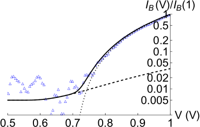
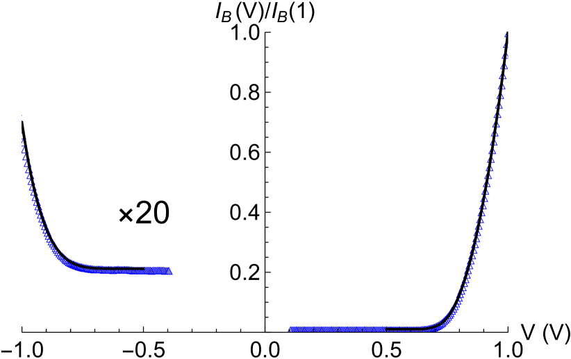
Finally, the width of the metal base determines not only the attenuation in that region but also the rate of creation for secondary Auger-like electrons near the onset, as can be seen in Figure 1-b comparing the blue and red curves where changes from negative to positive for . Doping of the semiconductor and the corresponding marginal layer’s width also plays a role since the intensity due to holes, in the opposite direction to Auger electrons, depends on these parameters. However, comparing results for samples 3 to 5 in Figures 9, 10, and 11, we conclude that the main parameter controlling the generation of Auger electrons corresponds to the width of the metal base. Given some mean free path , the probability for having an Auger process in some distance can be estimated as . The ratio of probabilities between a wide metal base, e.g. , to a thin one, , can be expanded for small x to obtain . To form an estimate we take Å (mean free path for inelastic processes in Au) and Å, which suggest that a wider metal base can have about times more probability to generate Auger processes, and therefore a corresponding stronger secondary current of electrons. Such is the case we observe in spectra 3, 4 and 5.
Since the relevant phase space here is related to the conduction band, we use again the value for injection of ballistic electrons and we add the probability of the inelastic loss that could create an Auger-like secondary electron, . Such value is close enough to the power we have used in Figure 1 to analyse the probability distribution of two barriers using the Bell-Kaiser model ( K), and it validates a posteriori the use of such an approximation. We recover two onsets, and eV, which are compatible with our previous findings for the injection of elastic ballistic electrons. The variation in the onsets with the different dopings is inside error bars, and we cannot confidently conclude about the dependence of the Schottky barrier with the semiconductor doping. However, the tendency for the onset values is compatible with what is expected. As revealed by k-space ab-initio Monte-Carlo simulation, electron-electron inelastic interaction opposes the focusing effect of diffraction due to the propagation through a periodic lattice and tends to defocus beams of secondary Auger electronsHohenester et al. (1997); de Andres et al. (2001). However, propagation of these electrons by more than ten layers of the metal base restore wavefunctions similar to the ones for ballistic electrons via the elastic interaction with the metallic periodic lattice, making these secondary electrons quite similar to the primary ones.
Finally, the semiconductor can also sustain Auger processes, but only for higher voltages, which are not relevant in our best-fit determination of that only uses a small interval of voltages near the onset. Therefore, these processes are not considered here.
IV Conclusions
We have developed an ab-initio phase-space formalism to describe currents of holes injected at negative voltages and secondary electrons formed via inelastic Auger processes. To that end, we have included the role of phonons interacting with holes probing the valence band and the Auger-like secondary beam, probing the conduction. Except for the ab-initio determination of the effective phase-space volume around the conduction band minima or the valence band maxima, the formalism is simple enough, as shown by Equation 1. It allows an accurate parameter-free determination of the onsets that characterize the Schottky barrier. Such an advantage over phenomenological models allows extracting Schottky barrier information from BEES in a technologically interesting but not-trivial situation, namely the two barriers found for injection of electrons in the conduction band in Au/Ge.
For the particular Au/Ge interface, we have found that direct injection of electrons into the conduction band shows two onsets at and eV, which agrees with our previous findings. Secondary Auger-like electrons injected into the conduction band also show two onsets at and eV, also in good agreement with our previous findings. However, for the injection of holes into the valence band, we have identified only a single onset at eV. Given the weakness of those currents, we cannot confidently conclude that this is a physical effect rather than the consequence of the higher noise-to-signal ratio.
Acknowledgments. This work was supported by the Spanish Ministry of Science (PID2020-113142RB-C21, MCIN/AEI/10.13039/501100011033). PdA acknowledges a Mobility Grant from the Spanish Ministry of Education.
References
- Sze and Kwok (2006) S. M. Sze and K. N. Kwok, Physics of Semiconductor Devices (John Wiley and Sons, 2006), ISBN 9780471143239.
- Bell and Kaiser (1988) L. D. Bell and W. J. Kaiser, Phys. Rev. Lett. 61, 2368 (1988).
- Bannani et al. (2008) A. Bannani, C. A. Bobisch, M. Matena, and R. Möller, Nanotechnology 19, 375706 (2008).
- Cook et al. (2015) M. Cook, R. Palandech, K. Doore, Z. Ye, G. Ye, R. He, and A. J. Stollenwerk, Phys. Rev. B 92, 201302 (2015).
- Wong et al. (2020) C. P. Y. Wong, C. Troadec, A. T. Wee, and K. E. J. Goh, Phys. Rev. Applied 14, 054027 (2020).
- Bell (2016) L. D. Bell, Journal of Vacuum Science & Technology B 34, 040801 (2016).
- Zhou et al. (2021) X. Zhou, K. Meng, T. Geng, J. Miao, X. Sun, and Q. Zhou, Organic Electronics 94, 106164 (2021), ISSN 1566-1199.
- Yi et al. (2009) W. Yi, A. Stollenwerk, and V. Narayanamurti, Surface Science Reports 64, 169 (2009), ISSN 0167-5729.
- Bobisch et al. (2009) C. A. Bobisch, A. Bannani, Y. M. Koroteev, G. Bihlmayer, E. V. Chulkov, and R. Möller, Phys. Rev. Lett. 102, 136807 (2009).
- Bobisch and Möller (2012) C. A. Bobisch and R. Möller, CHIMIA 66, 23 (2012).
- Qin et al. (2012) H. L. Qin, K. E. J. Goh, M. Bosman, K. L. Pey, and C. Troadec, Journal of Applied Physics 111, 013701 (2012).
- Parui et al. (2013) S. Parui, P. S. Klandermans, S. Venkatesan, C. Scheu, and T. Banerjee, Journal of Physics: Condensed Matter 25, 445005 (2013).
- Nolting et al. (2016) W. Nolting, C. Durcan, A. J. Narasimham, and V. P. LaBella, Journal of Vacuum Science & Technology B 34, 04J110 (2016).
- Wu et al. (2013) H. Wu, W. Huang, W. Lu, R. Tang, C. Li, H. Lai, S. Chen, and C. Xue, Applied Surface Science 284, 877 (2013), ISSN 0169-4332.
- Janardhanam et al. (2019) V. Janardhanam, H.-J. Yun, I. Jyothi, S.-H. Yuk, S.-N. Lee, J. Won, and C.-J. Choi, Applied Surface Science 463, 91 (2019), ISSN 0169-4332.
- Gerbi et al. (2020) A. Gerbi, R. Buzio, C. González, N. Manca, D. Marrè, S. Marras, M. Prato, L. Bell, S. Di Matteo, F. Flores, et al., ACS Applied Materials & Interfaces 12, 28894 (2020).
- Rogers et al. (2021) J. Rogers, W. Nolting, C. Durcan, R. Balsano, and V. P. LaBella, AIP Advances 11, 025108 (2021), eprint https://doi.org/10.1063/5.0038328, URL https://doi.org/10.1063/5.0038328.
- Claveau et al. (2017) Y. Claveau, S. D. Matteo, P. L. de Andres, and F. Flores, Journal of Physics: Condensed Matter 29, 115001 (2017).
- Lewis et al. (2011) J. P. Lewis, P. Jelinek, J. Ortega, A. A. Demkov, D. G. Trabada, B. Haycock, H. Wang, G. Adams, J. K. Tomfohr, E. Abad, et al., physica status solidi (b) 248, 1989 (2011).
- Gerbi et al. (2018) A. Gerbi, C. González, R. Buzio, N. Manca, D. Marrè, L. D. Bell, D. G. Trabada, S. Di Matteo, P. L. de Andres, and F. Flores, Phys. Rev. B 98, 205416 (2018).
- Balsano et al. (2013) R. Balsano, A. Matsubayashi, and V. P. LaBella, AIP Advances 3, 112110 (2013).
- Filatov et al. (2014) D. Filatov, D. Guseinov, I. Antonov, A. Kasatkin, and O. Gorshkov, RSC Adv. 4, 57337 (2014).
- Filatov et al. (2018) D. O. Filatov, D. V. Guseinov, V. Y. Chalkov, S. A. Denisov, and V. G. Shengurov, Semiconductors 52, 590 (2018).
- Reuter et al. (2000) K. Reuter, U. Hohenester, P. L. de Andres, F. J. García-Vidal, F. Flores, K. Heinz, and P. Kocevar, Phys. Rev. B 61, 4522 (2000).
- Bell et al. (1991) L. D. Bell, W. J. Kaiser, M. H. Hecht, and L. C. Davis, Journal of Vacuum Science and Technology B: Microelectronics and Nanometer Structures Processing, Measurement, and Phenomena 9, 594 (1991).
- Ludeke (1993a) R. Ludeke, Phys. Rev. Lett. 70, 214 (1993a).
- Hu et al. (2011) J. Hu, H.-S. P. Wong, and K. Saraswat, MRS Bull. 36, 112 (2011).
- Scappucci et al. (2013) G. Scappucci, G. Capellini, W. M. Klesse, and M. Y. Simmons, Nanoscale 5, 2600 (2013).
- Gerbi et al. (2014) A. Gerbi, R. Buzio, A. Gadaleta, L. Anghinolfi, M. Caminale, E. Bellingeri, A. S. Siri, and D. Marré, Advanced Materials Interfaces 1, 1300057 (2014).
- Buzio et al. (2018) R. Buzio, A. Gerbi, E. Bellingeri, and D. Marré, Applied Physics Letters 113, 141604 (2018).
- Buzio et al. (2020) R. Buzio, A. Gerbi, Q. He, Y. Qin, W. Mu, Z. Jia, X. Tao, G. Xu, and S. Long, Advanced Electronic Materials 6, 1901151 (2020).
- Ludeke (1993b) R. Ludeke, Journal of Vacuum Science and Technology A 11, 786 (1993b).
- Weisstein (2018) E. W. Weisstein, Polylogarithm, MathWorld – A Wolfram Web Resource (2018), http://mathworld.wolfram.com/Polylogarithm.html.
- Hervé et al. (2013a) M. Hervé, S. Tricot, Y. Claveau, G. Delhaye, B. Lépine, S. Di Matteo, P. Schieffer, and P. Turban, Applied Physics Letters 103, 202408 (2013a).
- Hervé et al. (2013b) M. Hervé, S. Tricot, S. Guézo, G. Delhaye, B. Lépine, P. Schieffer, and P. Turban, Journal of Applied Physics 113, 233909 (2013b).
- Prietsch and Ludeke (1991) M. Prietsch and R. Ludeke, Phys. Rev. Lett. 66, 2511 (1991).
- Hohenester et al. (1997) U. Hohenester, P. Kocevar, P. L. de Andres, and F. Flores, Phys. Stat. Sol. B 204, 397 (1997), cond-mat/9710151.
- de Andres et al. (2001) P. de Andres, F. Garcia-Vidal, K. Reuter, and F. Flores, Progress in Surface Science 66, 3 (2001), ISSN 0079-6816.
- Quinn (1962) J. J. Quinn, Phys. Rev. 126, 1453 (1962).
- Ladstädter et al. (2003) F. Ladstädter, P. F. de Pablos, U. Hohenester, P. Puschnig, C. Ambrosch-Draxl, P. L. de Andrés, F. J. García-Vidal, and F. Flores, Phys. Rev. B 68, 085107 (2003).
- Brown and Bray (1962) D. M. Brown and R. Bray, Phys. Rev. 127, 1593 (1962).
Appendix A Supplementary Information
A.1 Ab-initio determination of for hole injection
To determine the effective phase-space volume related to the injection of holes in the semiconductor valence band, we use our ab-initio approach to compute BEES I(V) for the interface Au/Ge under reverse bias conditions Gerbi et al. (2018). A critical point in this calculation is the band bending that appears on the semiconducting side. To simulate this effect, we have included a large number of layers ( Å) in the description of the semiconductor. The large depletion layer is connected to a bulk-like structure, obtained with the decimation technique Claveau et al. (2017), and the bending of bands has been modelled using quadratic interpolation. In our approach, the electronic states of each layer were shifted layer by layer in small energetic steps from the original position of the Fermi level at the interface to the final energy at the end of the intermediate area just before the semiconducting bulk. The resulting BEES curve was then fitted in the same way as previously explained for the injection of electrons Gerbi et al. (2018). For the pure ballistic current of holes (virtually no attenuation and K), we obtain for Au/Ge , cf. Figure 3.
A.2 Modification of due to phonons
Next, we study the attenuation of the ballistic current due to phonons which are the main source of attenuation in the low-energy region, as commented in Section III.2.
Let us consider the propagation through the marginal layer of a hole injected at the top of the valence band, . Any loss of energy due to quasi-elastic interactions with phonons should prevent the hole from getting to the bulk of the semiconductor. The probability for such a hole to traverse the width of the marginal layer, , without interacting with phonons is , where is the average rate of scattering with phonons determined by the mean free path . Therefore, we apply such probability as an attenuation factor for holes with energy in the interval , with a typical frequency for optical phonons ( eV).
We are interested in a small interval of energies near the onset which is helpful to obtain a best fit for the value for the Schottky barrier. In such an interval, e.g. eV, holes interacting with more than five phonons do not have enough energy to be injected into the valence band and can be neglected. Furthermore, in such a small interval of energies takes values that vary slowly and for the sake of simplicity can be approximated by its averaged value over that interval, Å.
We model the probability of the carrier interacting with phonons while being propagated through the marginal layer by a Poisson distribution,
| (3) |
where is the average mean rate of phonons expected in the length and is the greatest integer less than or equal to , i.e. the maximum number of possible phonons for each . Figure 4 compares with the power-law interpolating function , which justifies the use of up to eV to describe the quasi-elastic interaction between holes and phonons.

A.3 Modification of due to Auger electrons
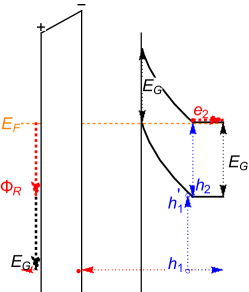
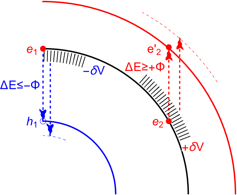
Figure 2 (bottom-left) shows an energy scheme for the generation of Auger electrons in the metal. A ballistic hole travelling with enough energy to be injected near the top of the valence band of the semiconductor () interacts inelastically with an electron near the Fermi surface transfering that energy to another electron , also near the Fermi surface, which uses the transferred energy to form a secondary electron with enough energy to be injected near the minimum of the conduction band. A qualitative argument based on the scheme displayed in Figure 5 shows how simultaneous conservation of momentum and energy for electrons inside an spherical shell of width recombining with holes , can transfer the right momentum and energy to electrons inside a spherical shell of width , to get enough energy to be injected near the minimum of the conduction band. Such a process increases the phase-space volume by the width of some spherical shell of width for and again for , hence . This qualitative argument agrees with the probability of inelastic interaction between electrons and so loses energy decaying to and can use it to be promoted to level . Such process has been computed long ago using the low-energy excitation spectra of free-electron metals by Quinn Quinn (1962). A full ab-initio calculation for Au and Pd by Ladstädter et al. Ladstädter et al. (2003) confirms Quinn’s arguments for free-electrons metals like Au. It becomes proportional to,
| (4) |
This value can be interpreted as the rate of energy loss due to Coulomb interaction, and yields again for in agreement with previous qualitative arguments in the literature Bell et al. (1991); Ludeke (1993b).
For the sake of completitude, Figure 2-(bottom-right) shows the corresponding energy scheme for the generation of Auger electrons in the semiconductor. Since this case only contributes to the current for , which is outside the interval of interest for our best-fit determination of , we do not include it in our calculations.
A.4 Ge
Here, we compute values for Ge at K and different doping leves that have been used in the paper. Sze and Kwok (2006)
For intrinsic Ge, the number of electrons in the conduction band at a given T is,
| (5) |
where is the Fermi-Dirac integral, and, is the effective density of states in the conduction band (T= 80 K),
| (6) |
where is the number of equivalent minima in the conduction band ( for Ge) and is the density of states effective mass for electrons ( for Ge, with the electron mass in vacuum). The number of holes near the top of the valence band, , is given by similar expressions, with (T= 80 K).
The intrinsic Fermi level is obtained by using . We have (T= 80 K),
| (7) |
where midgap is . The variation of the gap with temperature is described by the simple function, , which gives for K.
Finally, the intrinsic carrier density is (T=80 K).
For our heavily n-doped samples, is in the range to (0.001-0.01 cm). For these values the respective saturation temperatures are and K. Therefore, we are operating in the ionization regime and impurities dominate the conductivity of the semiconductor.
In the doped material the Fermi level adjusts to preserve charge neutrality, . Assuming that donor impurities with a concentration are located at below the conduction band ( eV for Au/Ge) we have,
| (8) |
Therefore, the charge neutrality condition reads,
| (9) |
which can be solved numerically, to obtain: eV for , eV for , and eV for .
Finally, we use Debye’s length, to estimate the size of the corresponding depletion layer. For Ge, ( the vacuum permitivity). At K we get Å for and Å for . For an abrupt junction, the inversion layer in Ge is estimated to be about .
The Fermi level moves from the low to the high doping sample closer to the conduction band by eV. This effect has not been seen in the corresponding values for the Schottky barrier because it falls inside error bars.
A.4.1 Mean free path of holes in Ge
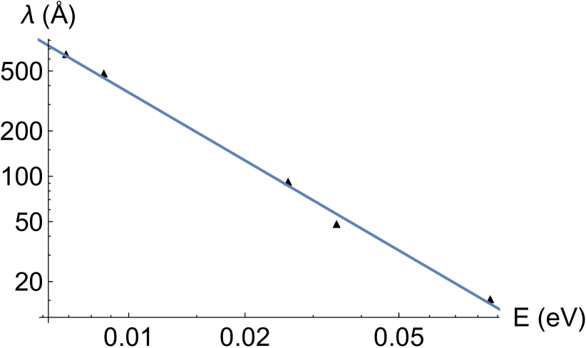
We derive values for the low-energy mean free path of holes injected in the semiconductor valence using values for the mobility reported by Brown and Bray Brown and Bray (1962),
| (10) |
Where and are the mass and charge of holes in the valence band and is a typical velocity used to convert lifetimes in mean free paths. Figure 6 shows how the mean free path changes from about Å for the typical optical phonon frequency of eV to about Å for the energy of five phonons, eV, which determines the interval of energies used in our analysis to determine the Schottky onset.
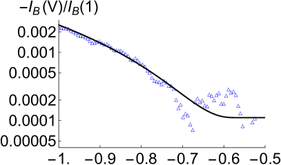
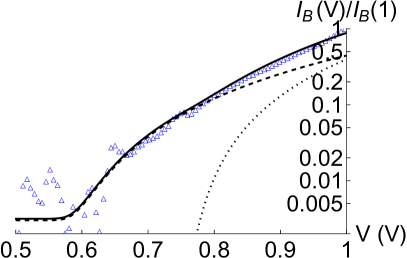
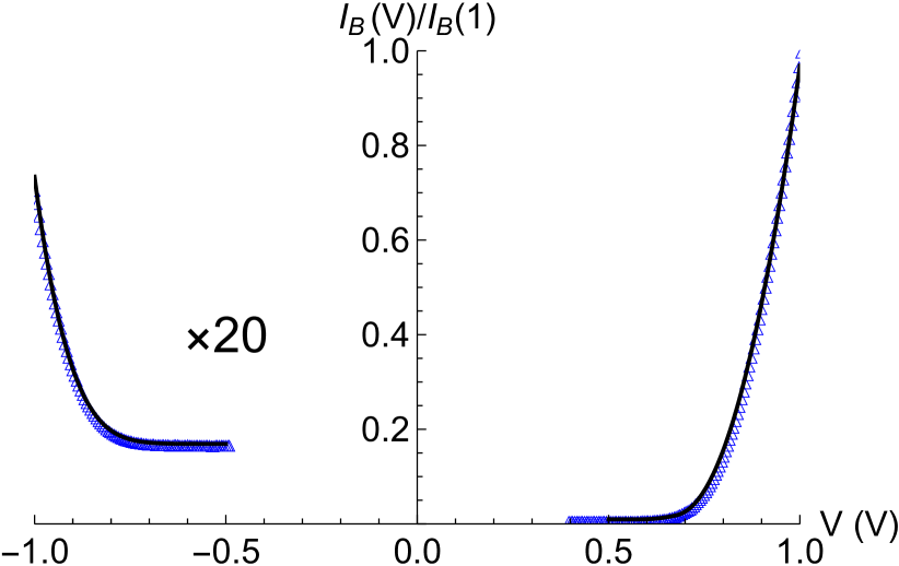
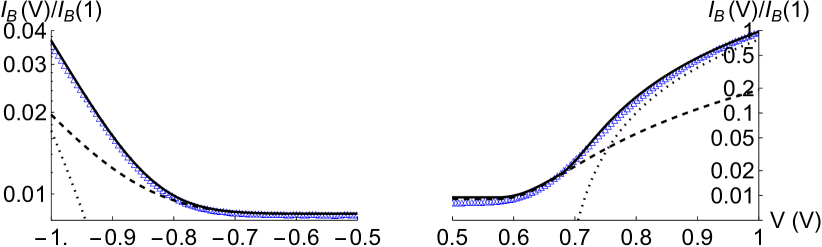
A.5 Best fits
Best fits for spectra 1 to 5 are shown in Figs. 7, 8, 9, 10 and, 11. The central sub-threshold region has been modelled as a constant noisy contribution that has been calculated by a simple average over the region, taken separately for positive and negative voltage. To facilitate the analysis the sub-threshold offset has been subtracted from the experimental data, and intensities have been normalized to the value to bring all data on a similar scale.