High-temperature Josephson diode
Abstract
Symmetry plays a critical role in determining various properties of a material. Semiconducting p-n junction diodes exemplify the engineered skew electronic response and are at the heart of contemporary electronic circuits. The non-reciprocal charge transport in a diode arises from doping-induced breaking of inversion symmetry. Breaking of time-reversal, in addition to inversion symmetry in some superconducting systems, leads to an analogous device – the superconducting diode. Following the pioneering first demonstration of the superconducting diode effect (SDE) [1], a plethora of new systems showing similar effects have been reported [2, 3, 4, 5, 6, 7, 8, 9, 10]. SDE lays the foundation for realizing ultra-low dissipative circuits, while Josephson phenomena-based diode effect (JDE) can enable realization of protected qubits [11, 12]. However, SDE and JDE reported thus far are at low temperatures ( K or lower) and impede their adaptation to technological applications. Here we demonstrate a Josephson diode working up to 77 K using an artificial Josephson junction (AJJ) of twisted layers of Bi2Sr2CaCu2O8+δ (BSCCO). The non-reciprocal response manifests as an asymmetry in the magnitude of switching currents as well as their distributions, and appears for all twist angles. The asymmetry is induced by and tunable with a very small magnetic field applied perpendicular to the junction. We report a record asymmetry of 60 % at 20 K. We explain our results within a vortex-based scenario. Our results provide a path toward realizing superconducting quantum circuits at liquid nitrogen temperature.
Introduction
Breaking of inversion and time-reversal symmetry is typically required to realize SDE [13]. Several proposals for realizing the superconducting analogue of the diode effect [14, 15, 16] have been explored. It was followed by successful demonstrations in various systems such as non-centrosymmetric superconductors [1, 2, 3], two-dimensional electron gases [4], patterned superconductors [5, 6], superconductor/ferromagnet multilayers [7, 8], and twisted graphene systems [9, 17]. Although several different mechanisms [3, 18, 19, 20, 21, 22] have been proposed to describe the observations across systems, the theories are still at their early stage of development. The SDE/JDE, which is the result of non-reciprocal response in these systems, manifests in terms of different magnitudes of superconducting switching currents () in the two opposite polarities. The effect has been demonstrated as magnetic field induced [1, 5, 6, 3, 2, 4] and field free [7, 8, 9] in nature. In terms of practical usability, however, all reports to date require very low temperatures, 4 K or less, to operate. We overcome this challenge using c-axis Josephson junctions (JJ) between flakes of a high- cuprate superconductor.
We demonstrate JDE in an artificially created Josephson junction (AJJ) by twisting two layers of BSCCO [23] that can be exfoliated to atomically flat flakes [24, 25, 26, 27] sustaining superconductivity down to the monolayer limit [28]. The difference between the magnitude of positive () and negative () switching currents and their statistical distributions, in these junctions, are tunable with a very small magnetic field applied perpendicular to the plane of the junction. The asymmetry persists from low temperature up to the superconducting transition temperature (, 77 K) of the junction and increases as temperature decreases, reaching a value as high as at 20 K. The diode behavior is demonstrated in terms of the half-wave rectification of a square wave current.
Heterostructures, assembled by twisting two layers of van der Waals materials offer a new platform for emergent electronic responses, entirely different from the constituent materials. In a similar spirit, a recent study [29] proposes the possibility of realizing time reversal symmetry broken high-temperature topological superconductivity at the interface of two 45° twisted BSCCO layers. Thus twisted BSCCO JJs offer a natural platform to explore the physics of JDE. Notably, our work demonstrates that JDE is a feature of the artificial c-axis JJs and does not require a special angle, 45°, as long as inversion symmetry is broken.
Fabricating twisted BSCCO junctions, however, is extremely challenging, and many of the junction properties are sensitive to fabrication methods. In the past, there have been numerous studies on artificially created twisted junctions of BSCCO to study the pairing symmetry of the superconducting order parameter. But the fabrication process involved high-temperature oxygen annealing to sustain the superconductivity at the interface. This led to observations of no [30, 31, 32] or different [33, 34] angular dependence of the Josephson coupling, different than the anticipated -wave superconductivity in BSCCO [35, 36]. Recently, there has been progress in making twisted BSCCO JJs using room temperature exfoliation [32, 34] and employing cryogenic exfoliation [37].
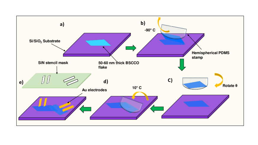
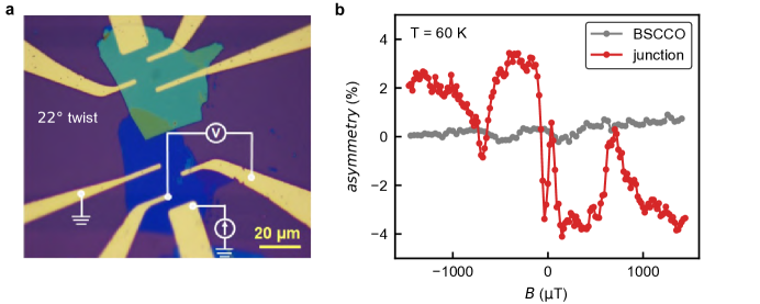
We fabricate twisted BSCCO JJs following Zhao et al. [37]. The junctions are created by re-exfoliating a relatively thicker BSCCO flake into two pieces and stacking them, which ensures alignment of the crystal axis and a well-defined twist angle (with an accuracy of ). The re-exfoliation is done inside an Ar-filled glove box with a low-temperature stage. To avoid any chemical contamination, Au contacts are directly deposited on the flake through a pre-aligned SiN mask. More details of the device fabrication are discussed in the methods section.
Experimental data
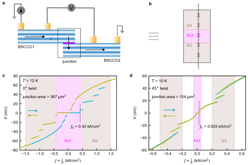
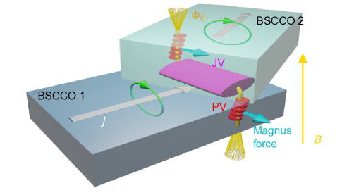
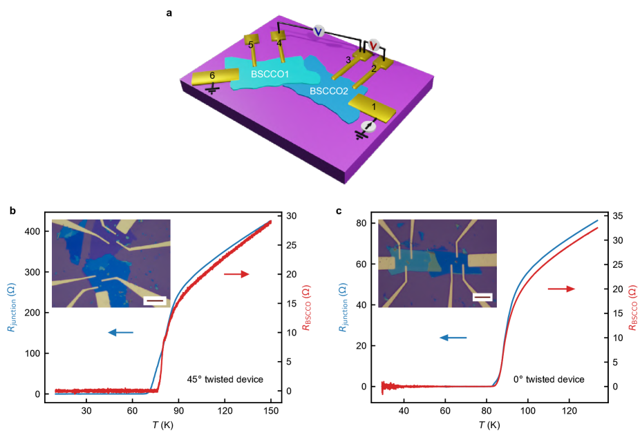
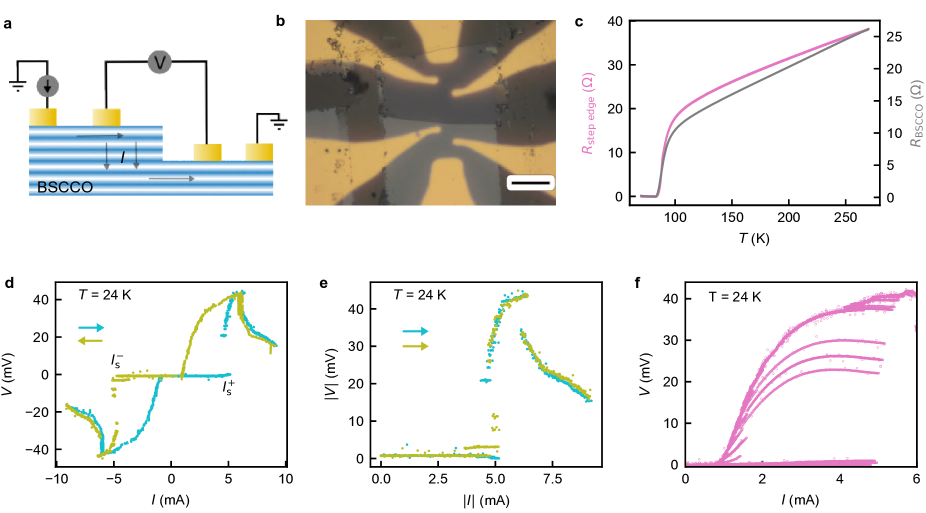
Fig. 1a and b show the schematic of the twisted BSCCO crystal structure and the device geometry of the artificial JJ, respectively. The crystal structure of BSCCO is such that it has its own IJJ. The superconducting Cu-O planes in this material, separated by the insulating SrO/BiO buffer layers (green slabs in Fig. 1a), are Josephson coupled and constitute a series of IJJs in the material structure [38]. By twisting two individual layers of BSCCO, we create an AJJ at the interface, as indicated in Fig. 1a. The twist angle controls [34, 37] the switching current density (), and consequently the Josephson energy, of the AJJs (maximum for 0°, and minimum for 45° twist) due to -wave symmetry of the superconducting order parameter in the system.
We made 10 AJJs with different twist angles (four 45°, four 0°, and two 22°). In the main text, we present data of one of 45° (D1) and 0° (D2) twisted junctions, and data of other twisted junctions are shown in Supplementary Information Fig. S6 and Extended Data Fig. 4 (22°, D5). The JDE is observed in all of the devices with different twist angles, an important aspect of our work. We design our devices such that we can simultaneously measure the junction properties and the two flakes that make the junction (Fig. 1b). We do this to ensure that there is no degradation during the fabrication. First, we check the four terminal resistance across the junction as a function of temperature which shows similar to the pristine BSCCO flake, as shown in the Supplementary Information, Fig. S3. The pristine nature of the fabricated junctions is evident from the fact that the 0° twisted junction has magnitude of switching current density () similar to the IJJs formed between the Cu-O planes in BSCCO (see Extended data Fig. 1).
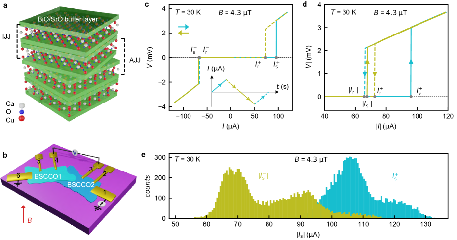
Fig. 1c shows across the junction at 30 K and at fixed µT, perpendicular to the junction plane (see Fig. 1b). Temperature dependence of is shown in Supplementary Information Fig. S11. We discuss the detailed field dependence later. The two colored line plots are for different sweep directions of the bias current as indicated by the arrows. The bias current is swept in the order as shown in the inset. We identify switching () and retrapping currents () in positive and negative bias range with and , as shown in Fig. 1c. The magnitude of is different from . The observed hysteresis between and is a well-understood physics of an underdamped JJ [39].
To clearly see the difference between the two switching currents and , we plot the curves of the negative bias branch by flipping their signs in Fig. 1d. From the plot, it is clear that is larger than . This means that at bias currents , , the system will dissipate energy and act like a resistive element in negative bias and be superconducting in positive bias. To quantify the difference between and we define an asymmetry factor, as . The value of for the data, shown in Fig. 1d at 30 K, is .
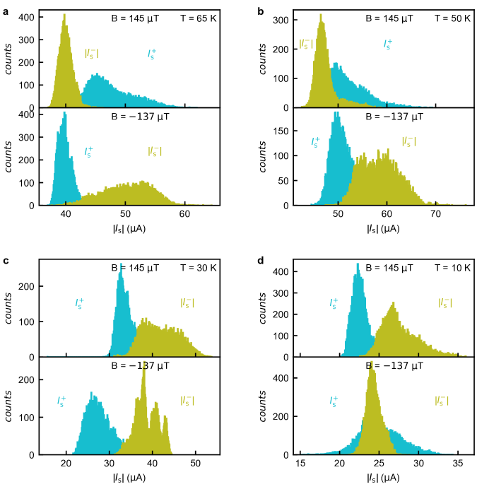
Switching of JJs from superconducting to resistive state is stochastic and has a finite distribution at a fixed temperature [40]. To probe the switching statistics for and in our twisted JJ, we measure switching events for both positive and negative bias currents and compare their distributions. The measurement protocol for switching distribution is discussed in the methods section. As seen in Fig. 1e, the median value of the distribution also shows asymmetry, as was seen in a single sweep. In addition, as we tune , the spread of the distributions becomes asymmetric – an aspect we discuss later.
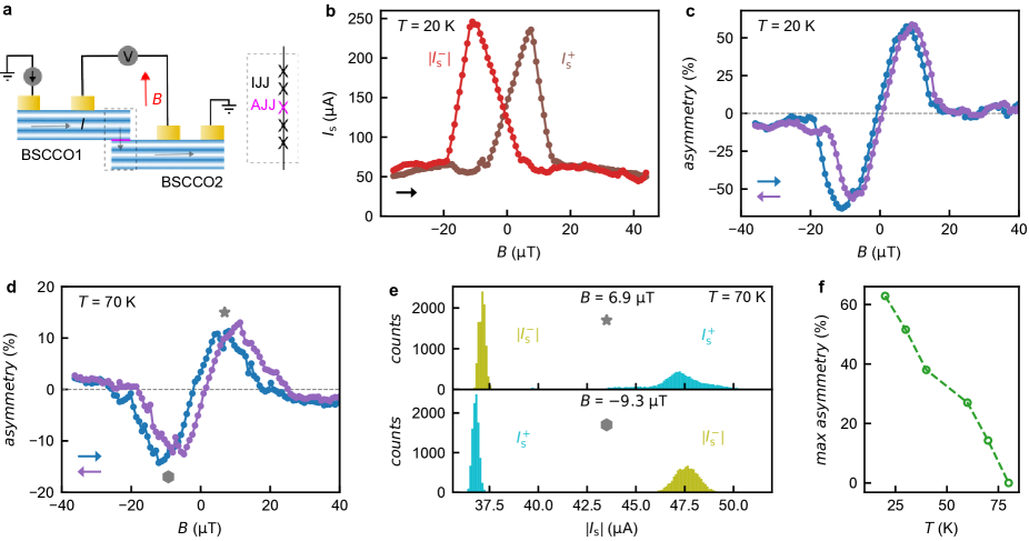
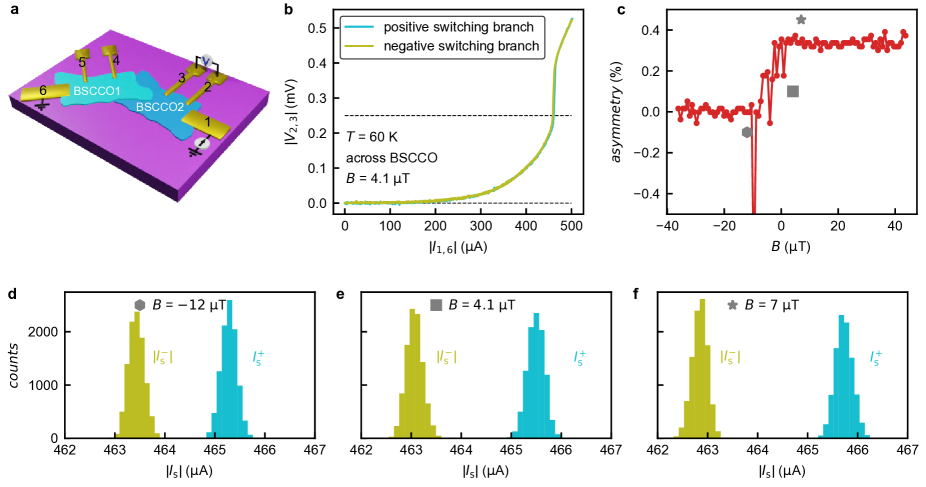
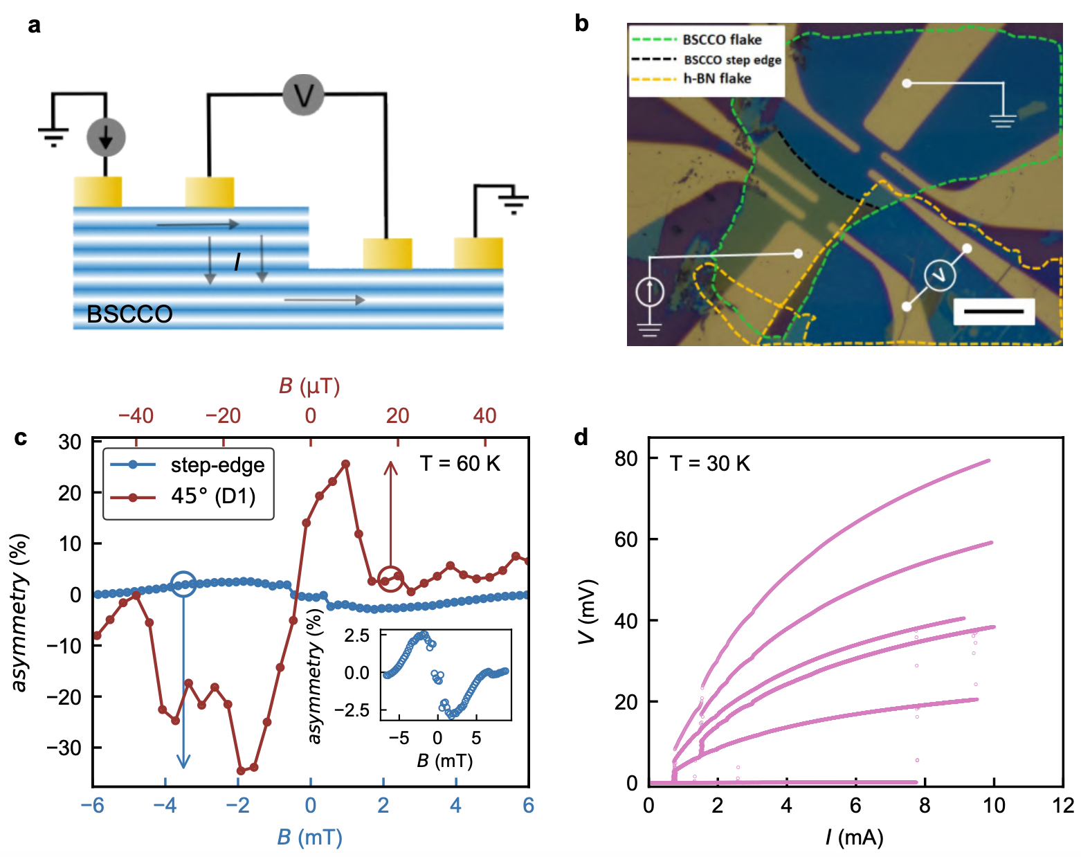
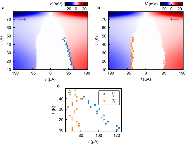
We next study the current asymmetry at different temperatures and with an external magnetic field , applied perpendicular to the plane of the junction. Fig. 2a shows the cross-sectional schematic of the device showing the IJJs formed between Cu-O planes and the AJJ, formed artificially. As depicted in Fig. 2a, the direction of the current across the AJJ is along the c-axis, parallel to applied . Fig. 2b shows the variation of and with at 20 K. At each value, we record 100 switching events with the help of a counter and average it out to get and , which are plotted in Fig. 2b. The measurement protocol is discussed in the methods section. Importantly, we note a pronounced change of and with a very small magnetic field. Variations of and show peaks that are shifted from each other along the axis. The difference in between the two peaks corresponds to a few flux quanta through the junction area. We calculate from this data. Fig. 2c,d show the evolution of calculated with at 20 and 70 K, respectively. The line plots with different colors are for two sweep directions of as indicated by the inset arrows. Here, we note the main observation. is antisymmetric in , and peaks at specific fields in both positive and negative directions of . This implies that is larger than at and smaller at . The field modulation of the asymmetry means that the effect we observe is field induced in nature and can be tuned/controlled by a very small magnetic field 10 µT. We have measured this device in cryogenic setup 1 using a homemade electromagnet to generate very small fields (see Supplementary Information, section S12 for details).
Additionally, we find the antisymmetric behavior with is not restricted to the magnitude of but is also reflected in the switching distribution widths of and . To see this, we record switching events for specific values (indicated in Fig. 2d by star and hexagon). Fig. 2e shows the distributions of the two switching currents in and at 70 K. From the plots, we clearly see the spread of the distribution for and is flipped with flipping the sign of . This behavior is present at all temperatures below (see Supplementary Information, Fig. S4).
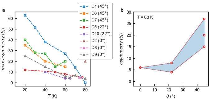
To see how varies with temperature, we determine its maximum value from the sweep at each temperature. The extracted value of maximum asymmetry is plotted with temperature in Fig. 2f. Importantly, the asymmetry persists till very close to and increases as the temperature is lowered below , reaching a value as high as at 20 K. This value of asymmetry factor is the highest reported so far at this temperature across systems showing SDE/JDE (see Supplementary Information, Section S4 for a comparison of the asymmetry factors and operating temperatures for different systems).
Half-wave rectification of the superconducting diode
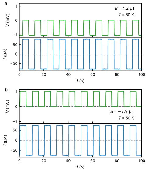
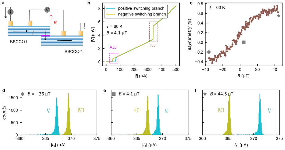
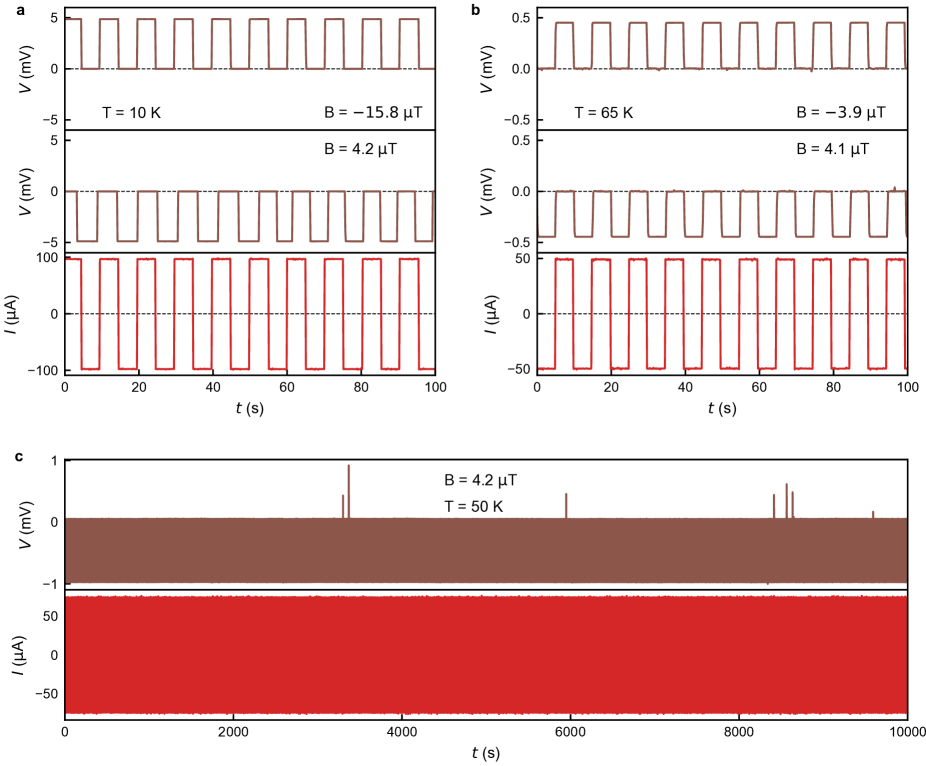
To show actual diode-like behavior, we demonstrate the half-wave rectification of an current. For that, we send a square wave excitation current of specific magnitude and frequency 0.1 Hz, and the voltage drop across the junction is measured. The magnitude of the current is such that it is larger than one of the switching currents ( or ) and smaller than the other. The results at 50 K are shown in Fig. 3. Rectification data at other temperatures are shown in Supplementary Information, Fig. S5. We see half-wave rectification of the negative half-cycle of the supercurrent at µT in Fig. 3a. By an externally applied , the asymmetry of switching currents can be reversed, which in turn changes the rectification nature of the junction. Fig. 3b shows rectification of the positive half-cycle of the supercurrent in presence of µT. The rectification ratio, as defined by , is very high () at 50 K.
Control experiments
All the observations described so far are exclusive to the AJJ at the interface of the two BSCCO flakes. We do several control checks to conclude this. We see negligibly small () and no significant effect of on switching current distributions for the pristine BSCCO flake in the same device away from the junction, as shown in the Extended data Fig. 2. Our device geometry and contacts configuration for the measurements are such that the measured response across the junction region includes junction properties at the interface as well as contributions from IJJs of bulk BSCCO flake, as seen in Fig. 2a. However, at smaller bias currents, only the artificial junction contributes by switching from superconducting to a normal state. As the current is increased further, the IJJs come into picture and switch one by one. Crucially, we observe asymmetry in of AJJs and small asymmetry () of IJJs in the same device. Also, the switching current distributions of IJJ do not show any tunability with applied . The data is shown in the Extended data Fig. 3. From all this evidence, it is very clear that the diode behavior arises from the artificial junction created by twisting two flakes of BSCCO at the interface.
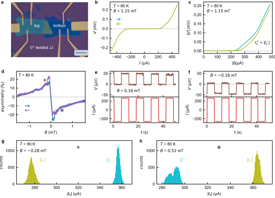
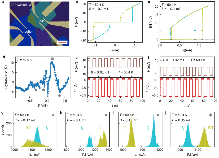
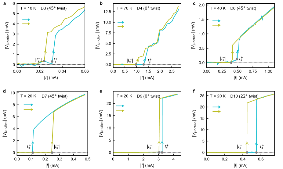
So far, we have discussed the results of a 45° twisted device, but the effect we see is not restricted to this specific twist angle. We observe the diode behavior in a 0° twisted device as well. Fig. 4a shows the optical image of the 0° twisted device, and Fig. 4b and c show the asymmetric nature of and . The asymmetry is tunable with (Fig. 4d), as was the case with the 45° twisted device discussed earlier. Fig. 4e and f show the rectification data at 80 K and its tunability with . In addition, the switching current distribution is tuned by . This indicates the key role of the magnetic field in the underlying mechanism of the JDE. Response of the 0° twisted device implies that the JDE effect is generic to AJJ at the interface and that the order-parameter symmetry does not play a significant role. However, the order parameter controls the magnitude of the switching current for different twist angles. The data from the 0° twisted device, where our alignment accuracy is , suggests that even the inadvertent breaking of interfacial inversion symmetry is crucial. As an additional control test, we fabricated a natural step-edge device where we see small switching current asymmetry (see Supplementary Information, Fig. S7 and S8). Moreover, the asymmetry is largest in twisted device and decreases with a decrease in twist angle (see Extended Data Fig. 5).
Importantly, we observe large asymmetry in our devices for out-of-plane and no asymmetry for in-plane (see Supplementary Information Fig. S13). For large in-plane we observe a typical Fraunhofer pattern for a JJ (see Supplementary Fig. S12). We note the out-of-plane range over which we see asymmetry tunability is smaller in twisted devices than devices (see table in section S11 in Supplementary Information).
Mechanisms for SDE
We now discuss possible mechanisms underlying the JDE in twisted BSCCO JJ (see Extended data Fig. 6 for a schematic and Supplementary Information section S17 for additional details). The data indicate that the diode response originates from the interface between top and bottom crystals (AJJ). This interface breaks inversion symmetry due to misalignment of crystal axes as well as uncorrelated defect distributions. Moreover, the diode response occurs when applying a magnetic field, which breaks time-reversal symmetry. Along with the observation of a stronger asymmetry in switching than retrapping, this suggests an origin in the current-phase relation [41].
We estimate that the Josephson penetration depth ( µm) is large compared to the width of the junctions [37]. In this situation, the spatial dependence of the gauge-invariant phase difference across the AJJ is governed by the externally applied magnetic field. The phase difference depends on the magnetic-field component parallel to the plane as well as differences in vortex configuration between the top and bottom flakes. The critical current of the junction is governed by the resulting Fraunhofer-like interference [39].
In the experiment, the field is applied along the -axis. As the London penetration depth µm is small compared to the width of the flakes, this field induces stacks of pancake vortices in the top and/or bottom flakes of the junction. The stacks will tend to pin at different locations in top and bottom flake due to uncorrelated defect configurations. At the AJJ, the magnetic flux of these vortex stacks either escapes or connects (via a Josephson vortex) within the plane [42, 43, 44, 45]. The difference in the vortex configurations as well as the field along the -plane (Josephson vortex) generate a spatially dependent phase difference, affecting the critical current of the junction (see Extended data Fig. 6). From the sample geometry, we see the bias current has a component flowing in the plane. This current induces an asymmetry in the switching current due to the associated magnetic field in the plane and the resulting Magnus force acting on the stacks of pancake vortices. The induced field modifies the Fraunhofer interference asymmetrically in bias-current direction [46]. We estimate a resulting asymmetry in the percent range, considerably below the maximal observed asymmetries (see Supplementary Information section S18C for details). Larger asymmetries can be induced by Magnus forces on the vortex stacks by the bias current. This force acts in opposite directions for the two bias directions, inducing significant and asymmetric rearrangements of the vortex configuration, with a concurrent change of the Fraunhofer interference.
This scenario is consistent with the central observations: (i) The asymmetry sets in at low fields when the first vortices enter along the -axis. With increasing , the variation in phase difference increases along with the number of vortices, reducing the amplitude of the Fraunhofer interference and hence the asymmetry. (ii) Fields along the -axis are effectively focused into the -plane. No corresponding focusing occurs for fields applied along the -plane due to the much larger and smaller sample cross-section. This explains the absence of asymmetry when applying the field along the -plane. (iii) With increasing twist angle, the Josephson coupling between vortex stacks in top and bottom flakes weakens due to the -wave nature of superconductivity. This implies weaker correlations between vortices in the bottom and top flakes and thus larger variations in the phase difference, explaining the trend to lower onset fields as the twist angle increases. (iv) Vortex pinning induces a weakly hysteretic -field dependence of the asymmetry, as regularly observed. (v) Multistabilities of the vortex configuration induce asymmetry and multiple humps in the distribution of the switching current.
Vortex-induced mechanisms have also been discussed for diode effects in the bulk critical current of thin-film superconductors [47, 48]. While the critical current of our junctions is governed by Fraunhofer interference, it is controlled by vortex flow (and asymmetric edge barriers for vortices [49, 50, 51]) in the case of the superconducting thin films. We note that a possible edge barrier effect is very small in our samples as we observe only weak asymmetry ( %) in pristine BSCCO flakes in the same device away from the junction. We can also eliminate a contribution coming from magnetochiral anisotropy (MCA) [1] in our case as we see JDE with parallel to both the current flowing directions () and the axis of broken inversion symmetry at the junction.
Conclusions
In summary, we report and explain the Josephson diode effect in artificially created Josephson junctions of twisted BSCCO. Our work demonstrates the highest asymmetry in magnitudes of switching currents reported so far of at 20 K. While the magnitude of the switching current is tuned by twist angle and sets the Josephson energy of these junctions, the asymmetry on the other hand is tuned by an independent knob – a very small magnetic field ( 10 µT) applied perpendicular to the junction plane. The asymmetry persists even at 80 K for some twist angles. Demonstration of Josephson diode effect above liquid nitrogen boiling point (77 K) is a significant advancement that will ease its adaptation to real applications in circuits with ultra-low dissipation. The required small fields to tune asymmetry can be generated on-chip allowing greater design flexibility. Protected qubits [11, 12] based on the Josephson diode operating at higher temperatures could lead to a new architecture for quantum devices.
Methods
Device fabrication
We developed the cryogenic exfoliation setup for fabrication of the BSCCO Josephson junctions. It is a completely dry pick-up and transfer method and can be employed to exfoliate various 2D materials. The cryogenic exfoliation technique allows re-exfoliation of a relatively thicker BSCCO flake, which is pre-exfoliated on a Si/SiO2 chip. Re-exfoliation from the same flake ensures the alignment of the crystal axis. The re-exfoliated flake is rotated by a specific angle and immediately transferred onto the same flake to form a twisted junction. The low-temperature exfoliation method is very efficient in preventing the degradation of interfacial superconductivity.
Inside an Ar-filled glove box, we exfoliate BSCCO from an optimally doped bulk crystal by scotch tape technique on plasma-cleaned Si/SiO2 substrate. The Si/SiO2 substrate is heated inside the Ar-filled glove box overnight before exfoliation to remove any adsorbed gases. The substrate with exfoliated BSCCO is then placed on a cold stage under a microscope. We pass liquid nitrogen through the stage to cool it. Once the temperature of the stage reaches C, we attach hemispherical polydimethylsiloxane (PDMS) stamp with the appropriately identified thicker BSCCO flake. The temperature of the stage is lowered further. At around C the PDMS stamp goes through its glass transition point. Consequently, it gets detached automatically from the substrate by partially cleaving thick BSCCO flake into two pieces. Next, we quickly rotate the upper stage on which PDMS is mounted by a specified angle (with accuracy) and re-assemble it. The cold stage is then warmed slowly to C and the hemispherical stamp is detached. After the stack reaches room temperature, we take it out and align it with a SiN mask inside a clean room for contact deposition. 70 nm Au contacts are deposited by e-beam evaporation. For more details on cryogenic exfoliation, see Supplementary Information, Section S1. The thicknesses of all measured devices are tabulated in Supporting Information, section S11.
Measurements
dc I-V measurements
voltage from NI DAQ is fed to a series resistor (10 k). The outcoming current is sent through the device by the current injecting electrode. The current is then collected by a current-to-voltage converter and measured with NI DAQ. The voltage drop across the device is also measured with the DAQ after amplification by a voltage preamplifier.
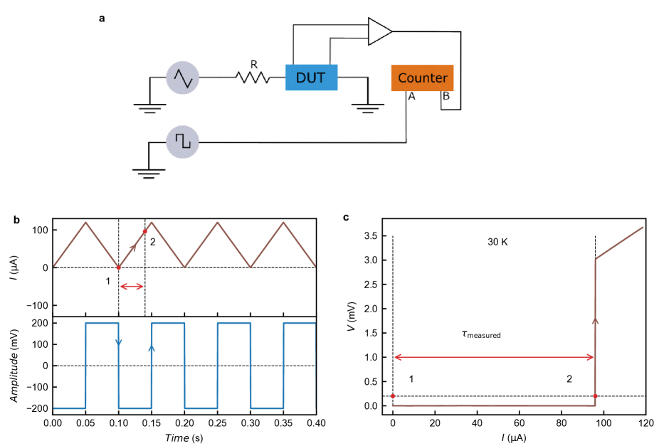
Measurement of switching current distributions
For distributions of switching currents with switching events, we employ a counter (Tektronix FCA 3100) for faster measurements. A symmetric triangular wave current (larger than ) of frequency 10 Hz from a Keysight 33600A function generator is sent through the device. A offset current is added to the triangular current. The offset makes the triangular current go from to or to . The minimum and maximum value of the triangular current ensures the device switches from superconducting to the normal state and again returns to the superconducting state in each cycle of the triangular current. The counter measures the time interval between two events – when the voltage drop across the device is zero at and when it reaches a non-zero pre-defined value because of switching from superconducting to normal state. From the measured time interval, we convert it to switching currents ( and ). More details are provided in Supplementary Information, Section S2.
Measurement of switching currents with
Instead of taking single curves and finding out and , we take 100 switching events with a counter and average them to get and at each . Here, is the slow axis for the measurement. A homemade electromagnet was used to get a very small . The device, along with the electromagnet, was enclosed inside a cryoperm box to shield the device from outside stray fields. Extreme care has been taken to calibrate the actual fields inside the shielded cryoperm box. Details are provided in Supplementary Information, section S12.
Data availability
The data supporting the findings of this study are available from the corresponding authors upon reasonable request.
References
- [1] Ando, F. et al. Observation of superconducting diode effect. Nature 584, 373–376 (2020). URL https://www.nature.com/articles/s41586-020-2590-4. Number: 7821 Publisher: Nature Publishing Group.
- [2] Zhang, E. et al. Nonreciprocal superconducting NbSe2 antenna. Nature Communications 11, 5634 (2020). URL https://www.nature.com/articles/s41467-020-19459-5. Number: 1 Publisher: Nature Publishing Group.
- [3] Wakatsuki, R. et al. Nonreciprocal charge transport in noncentrosymmetric superconductors. Science Advances 3, e1602390 (2017). URL https://www.science.org/doi/10.1126/sciadv.1602390. Publisher: American Association for the Advancement of Science.
- [4] Baumgartner, C. et al. Supercurrent rectification and magnetochiral effects in symmetric Josephson junctions. Nature Nanotechnology 17, 39–44 (2022). URL https://www.nature.com/articles/s41565-021-01009-9. Number: 1 Publisher: Nature Publishing Group.
- [5] Lyu, Y.-Y. et al. Superconducting diode effect via conformal-mapped nanoholes. Nature Communications 12, 2703 (2021). URL https://www.nature.com/articles/s41467-021-23077-0. Number: 1 Publisher: Nature Publishing Group.
- [6] Bauriedl, L. et al. Supercurrent diode effect and magnetochiral anisotropy in few-layer NbSe2. Nature Communications 13, 4266 (2022). URL https://www.nature.com/articles/s41467-022-31954-5. Number: 1 Publisher: Nature Publishing Group.
- [7] Narita, H. et al. Field-free superconducting diode effect in noncentrosymmetric superconductor/ferromagnet multilayers. Nature Nanotechnology (2022). URL https://www.nature.com/articles/s41565-022-01159-4.
- [8] Wu, H. et al. The field-free Josephson diode in a van der Waals heterostructure. Nature 604, 653–656 (2022). URL https://www.nature.com/articles/s41586-022-04504-8. Number: 7907 Publisher: Nature Publishing Group.
- [9] Lin, J.-X. et al. Zero-field superconducting diode effect in small-twist-angle trilayer graphene. Nature Physics 1–7 (2022). URL https://www.nature.com/articles/s41567-022-01700-1. Publisher: Nature Publishing Group.
- [10] Trahms, M. et al. Diode effect in Josephson junctions with a single magnetic atom. Nature 1–6 (2023). URL https://www.nature.com/articles/s41586-023-05743-z. Publisher: Nature Publishing Group.
- [11] Larsen, T. et al. Parity-Protected Superconductor-Semiconductor Qubit. Physical Review Letters 125, 056801 (2020). URL https://link.aps.org/doi/10.1103/PhysRevLett.125.056801. Publisher: American Physical Society.
- [12] Schrade, C., Marcus, C. M. & Gyenis, A. Protected Hybrid Superconducting Qubit in an Array of Gate-Tunable Josephson Interferometers. PRX Quantum 3, 030303 (2022). URL https://link.aps.org/doi/10.1103/PRXQuantum.3.030303. Publisher: American Physical Society.
- [13] Tokura, Y. & Nagaosa, N. Nonreciprocal responses from non-centrosymmetric quantum materials. Nature Communications 9, 3740 (2018). URL https://www.nature.com/articles/s41467-018-05759-4. Number: 1 Publisher: Nature Publishing Group.
- [14] Hu, J., Wu, C. & Dai, X. Proposed Design of a Josephson Diode. Physical Review Letters 99, 067004 (2007). URL https://link.aps.org/doi/10.1103/PhysRevLett.99.067004. Publisher: American Physical Society.
- [15] Chen, C.-Z. et al. Asymmetric Josephson effect in inversion symmetry breaking topological materials. Physical Review B 98, 075430 (2018). URL https://link.aps.org/doi/10.1103/PhysRevB.98.075430. Publisher: American Physical Society.
- [16] Misaki, K. & Nagaosa, N. Theory of the nonreciprocal Josephson effect. Physical Review B 103, 245302 (2021). URL https://link.aps.org/doi/10.1103/PhysRevB.103.245302. Publisher: American Physical Society.
- [17] Diez-Merida, J. et al. Magnetic Josephson Junctions and Superconducting Diodes in Magic Angle Twisted Bilayer Graphene (2021). URL http://arxiv.org/abs/2110.01067. ArXiv:2110.01067 [cond-mat].
- [18] Yuan, N. F. Q. & Fu, L. Supercurrent diode effect and finite-momentum superconductors. Proceedings of the National Academy of Sciences 119, e2119548119 (2022). URL https://www.pnas.org/doi/full/10.1073/pnas.2119548119. Publisher: Proceedings of the National Academy of Sciences.
- [19] Daido, A., Ikeda, Y. & Yanase, Y. Intrinsic Superconducting Diode Effect. Physical Review Letters 128, 037001 (2022). URL https://link.aps.org/doi/10.1103/PhysRevLett.128.037001.
- [20] Davydova, M., Prembabu, S. & Fu, L. Universal Josephson diode effect. Science Advances 8, eabo0309 (2022). URL https://www.science.org/doi/full/10.1126/sciadv.abo0309. Publisher: American Association for the Advancement of Science.
- [21] Zhang, Y., Gu, Y., Li, P., Hu, J. & Jiang, K. General Theory of Josephson Diodes. Physical Review X 12, 041013 (2022). URL https://link.aps.org/doi/10.1103/PhysRevX.12.041013. Publisher: American Physical Society.
- [22] Tanaka, Y., Lu, B. & Nagaosa, N. Theory of giant diode effect in $d$-wave superconductor junctions on the surface of a topological insulator. Physical Review B 106, 214524 (2022). URL https://link.aps.org/doi/10.1103/PhysRevB.106.214524. Publisher: American Physical Society.
- [23] Maeda, H., Tanaka, Y., Fukutomi, M. & Asano, T. A New High-Tc Oxide Superconductor without a Rare Earth Element. Japanese Journal of Applied Physics 27, L209 (1988). URL https://iopscience.iop.org/article/10.1143/JJAP.27.L209/meta. Publisher: IOP Publishing.
- [24] Liao, M. et al. Superconductor–Insulator Transitions in Exfoliated Flakes. Nano Letters 18, 5660–5665 (2018). URL https://doi.org/10.1021/acs.nanolett.8b02183. Publisher: American Chemical Society.
- [25] Sterpetti, E., Biscaras, J., Erb, A. & Shukla, A. Comprehensive phase diagram of two-dimensional space charge doped . Nature Communications 8, 2060 (2017). URL https://www.nature.com/articles/s41467-017-02104-z. Number: 1 Publisher: Nature Publishing Group.
- [26] Zhao, S. F. et al. Sign-Reversing Hall Effect in Atomically Thin High-Temperature Superconductors. Physical Review Letters 122, 247001 (2019). URL https://link.aps.org/doi/10.1103/PhysRevLett.122.247001. Publisher: American Physical Society.
- [27] Ghosh, S. et al. On-Demand Local Modification of High-Tc Superconductivity in Few Unit-Cell Thick . Advanced Materials 32, 2002220 (2020). URL https://onlinelibrary.wiley.com/doi/abs/10.1002/adma.202002220. _eprint: https://onlinelibrary.wiley.com/doi/pdf/10.1002/adma.202002220.
- [28] Yu, Y. et al. High-temperature superconductivity in monolayer . Nature 575, 156–163 (2019). URL https://www.nature.com/articles/s41586-019-1718-x. Number: 7781 Publisher: Nature Publishing Group.
- [29] Can, O. et al. High-temperature topological superconductivity in twisted double-layer copper oxides. Nature Physics 17, 519–524 (2021). URL https://www.nature.com/articles/s41567-020-01142-7. Number: 4 Publisher: Nature Publishing Group.
- [30] Li, Q. et al. Bicrystal -Axis Twist Josephson Junctions: A New Phase-Sensitive Test of Order Parameter Symmetry. Physical Review Letters 83, 4160–4163 (1999). URL https://link.aps.org/doi/10.1103/PhysRevLett.83.4160. Publisher: American Physical Society.
- [31] Latyshev, Y. I., Orlov, A. P., Nikitina, A. M., Monceau, P. & Klemm, R. A. -axis transport in naturally grown cross-whisker junctions. Physical Review B 70, 094517 (2004). URL https://link.aps.org/doi/10.1103/PhysRevB.70.094517. Publisher: American Physical Society.
- [32] Zhu, Y. et al. Presence of -Wave Pairing in Josephson Junctions Made of Twisted Ultrathin Flakes. Physical Review X 11, 031011 (2021). URL https://link.aps.org/doi/10.1103/PhysRevX.11.031011. Publisher: American Physical Society.
- [33] Takano, Y. et al. d-like symmetry of the order parameter and intrinsic Josephson effects in cross-whisker junctions. Physical Review B 65, 140513 (2002). URL https://link.aps.org/doi/10.1103/PhysRevB.65.140513. Publisher: American Physical Society.
- [34] Lee, J. et al. Twisted van der Waals Josephson Junction Based on a High-Tc Superconductor. Nano Letters 21, 10469–10477 (2021). URL https://doi.org/10.1021/acs.nanolett.1c03906. Publisher: American Chemical Society.
- [35] Shen, Z.-X. et al. Anomalously large gap anisotropy in the a-b plane of . Physical Review Letters 70, 1553–1556 (1993). URL https://link.aps.org/doi/10.1103/PhysRevLett.70.1553. Publisher: American Physical Society.
- [36] Gu, Q. et al. Directly visualizing the sign change of d-wave superconducting gap in by phase-referenced quasiparticle interference. Nature Communications 10, 1603 (2019). URL https://www.nature.com/articles/s41467-019-09340-5. Number: 1 Publisher: Nature Publishing Group.
- [37] Zhao, S. Y. F. et al. Emergent Interfacial Superconductivity between Twisted Cuprate Superconductors. Tech. Rep. arXiv:2108.13455, arXiv (2021). URL http://arxiv.org/abs/2108.13455. ArXiv:2108.13455 [cond-mat] type: article.
- [38] Kleiner, R., Steinmeyer, F., Kunkel, G. & Müller, P. Intrinsic Josephson effects in single crystals. Physical Review Letters 68, 2394–2397 (1992). URL https://link.aps.org/doi/10.1103/PhysRevLett.68.2394. Publisher: American Physical Society.
- [39] Tinkham, M. Introduction to Superconductivity (Courier Corporation, 2004). Google-Books-ID: VpUk3NfwDIkC.
- [40] Fulton, T. A. & Dunkleberger, L. N. Lifetime of the zero-voltage state in Josephson tunnel junctions. Physical Review B 9, 4760–4768 (1974). URL https://link.aps.org/doi/10.1103/PhysRevB.9.4760. Publisher: American Physical Society.
- [41] Steiner, J. F., Melischek, L., Trahms, M., Franke, K. J. & von Oppen, F. Diode effects in current-biased Josephson junctions (2022). URL http://arxiv.org/abs/2212.06866. ArXiv:2212.06866 [cond-mat].
- [42] Golubov, A. A. & Ustinov, A. V. Interaction energy of Abrikosov and Josephson vortices in a long Josephson junction. Physics Letters A 162, 409–414 (1992). URL https://www.sciencedirect.com/science/article/pii/037596019290064S.
- [43] Blatter, G., Feigel’man, M. V., Geshkenbein, V. B., Larkin, A. I. & Vinokur, V. M. Vortices in high-temperature superconductors. Reviews of Modern Physics 66, 1125–1388 (1994). URL https://link.aps.org/doi/10.1103/RevModPhys.66.1125. Publisher: American Physical Society.
- [44] Grigorenko, A., Bending, S., Tamegai, T., Ooi, S. & Henini, M. A one-dimensional chain state of vortex matter. Nature 414, 728–731 (2001). URL https://www.nature.com/articles/414728a. Number: 6865 Publisher: Nature Publishing Group.
- [45] Cole, D. et al. Ratchet without spatial asymmetry for controlling the motion of magnetic flux quanta using time-asymmetric drives. Nature Materials 5, 305–311 (2006). URL https://www.nature.com/articles/nmat1608.
- [46] Golod, T. & Krasnov, V. M. Demonstration of a superconducting diode-with-memory, operational at zero magnetic field with switchable nonreciprocity. Nature Communications 13, 3658 (2022). URL https://www.nature.com/articles/s41467-022-31256-w. Number: 1 Publisher: Nature Publishing Group.
- [47] Hou, Y. et al. Ubiquitous Superconducting Diode Effect in Superconductor Thin Films. Tech. Rep. arXiv:2205.09276, arXiv (2022). URL http://arxiv.org/abs/2205.09276. ArXiv:2205.09276 [cond-mat] type: article.
- [48] Brandt, E. H. Thin superconductors and SQUIDs in perpendicular magnetic field. Physical Review B 72, 024529 (2005). URL https://link.aps.org/doi/10.1103/PhysRevB.72.024529. Publisher: American Physical Society.
- [49] Vodolazov, D. Y. & Peeters, F. M. Superconducting rectifier based on the asymmetric surface barrier effect. Physical Review B 72, 172508 (2005). URL https://link.aps.org/doi/10.1103/PhysRevB.72.172508. Publisher: American Physical Society.
- [50] Sivakov, A. G., Turutanov, O. G., Kolinko, A. E. & Pokhila, A. S. Spatial characterization of the edge barrier in wide superconducting films. Low Temperature Physics 44, 226–232 (2018). URL https://aip.scitation.org/doi/full/10.1063/1.5024540. Publisher: American Institute of Physics.
- [51] Suri, D. et al. Non-reciprocity of vortex-limited critical current in conventional superconducting micro-bridges. Applied Physics Letters 121, 102601 (2022). URL https://aip.scitation.org/doi/full/10.1063/5.0109753. Publisher: American Institute of Physics.
- [52] Pal, B. et al. Josephson diode effect from Cooper pair momentum in a topological semimetal. Nature Physics 1–6 (2022). URL https://www.nature.com/articles/s41567-022-01699-5. Publisher: Nature Publishing Group.
- [53] Shin, J. et al. Magnetic Proximity-Induced Superconducting Diode Effect and Infinite Magnetoresistance in van der Waals Heterostructure (2021). URL http://arxiv.org/abs/2111.05627. ArXiv:2111.05627 [cond-mat].
- [54] Hänggi, P., Talkner, P. & Borkovec, M. Reaction-rate theory: fifty years after kramers. Rev. Mod. Phys. 62, 251–341 (1990). URL https://link.aps.org/doi/10.1103/RevModPhys.62.251.
Acknowledgments
We thank Eli Zeldov, Abhay Pasupathy, Vibhor Singh, Pratap Raychaudhuri, Satyajit Banerjee, Sophie Gueron, Hélène Bouchiat, R. Vijay, Vladimir Krasnov, Subhajit Sinha, and Joydip Sarkar for helpful discussions and comments. We thank Amit P. Shah for his help in making SiN membranes for shadow masks. We acknowledge Department of Science and Technology (DST), Nanomission grant SR/NM/NS-45/2016, CORE grant CRG/2020/003836, and Department of Atomic Energy (DAE) of Government of India 12-R&D-TFR-5.10-0100 for support. Work in Berlin was supported by Deutsche Forschungsgemeinschaft through CRC 183 (project C02) as well as TWISTGRAPH.
Author contributions
S.G. and V.P. fabricated the devices. A.B., K. and A.D. helped in device fabrication. S.G. and A.B. did the measurements. D.A.J., R.K., and A.T. grew the BSCCO crystals. J.F.S. and F.v.O. developed the theoretical interpretation. S.G., F.v.O. and M.M.D. wrote the manuscript. All authors provided inputs to the manuscript. M.M.D. supervised the project.
Competing interests
The authors declare no competing financial interests.
Supplementary Information: High-temperature Josephson diode
S1 Cryogenic exfoliation to make twisted BSCCO JJ
Some 2D materials are chemically unstable in the atmosphere. Therefore, the device fabrication of those 2D materials is challenging. In this work, we developed cryogenic exfoliation, pick-up, and transfer methods for 2D materials following Zhao et al. [37]. BSCCO degrades with time; hence we used hemispherical PDMS dry transfer techniques for the twisted device fabrication in the glove box environment. The hemispherical PDMS stamp is made using Sigma Aldrich Sylgard 184 silicon elastomer base and curing agent mixture with a ratio of 10:1. After that, we cut Gel-Pak (part no- 40x40-0170-X4) PDMS into cylindrical pieces with a diameter of mm and put the viscous mixture of Sylgard 184 on those pieces, then baked at 100° C for 15 min. For the exfoliation of BSCCO crystal, we used a Si/SiO2 substrate, which was cleaned by O2 plasma for 90 s and heated at 150° C overnight. Then we exfoliate BSSCO (Bi-2212) crystal by the mechanical scotch tape method and transfer the exfoliated BSCCO flake onto the pre-cleaned Si/SiO2 substrate. Then we put the substrate on the cryogenic stage and search for thick ( 40-60 nm), flat, and uniform BSCCO flake through the optical microscope. Once we identify the desired flake, we cool down the cryogenic setup using liquid nitrogen. When the temperature reaches C, we attach a hemispherical PDMS stamp to the BSCCO flake and wait for the temperature to reach C. At this temperature, the PDMS goes through the glass transition state. Because of that, the PDMS meniscus automatically detaches from the BSCCO flake. During this detachment, some part of the flake cleaves and attaches to the PDMS stamp. Then we quickly rotate the PDMS stamp at an angle (with an accuracy of ) and drop the PDMS-attached BSCCO flake on top of the bottom flake, as shown in Fig. S1. Then, we warm the cold stage to C and slowly remove the hemispherical PDMS stamp. Finally, we align a SiN mask with the flakes and deposit 70 nm thick gold (Au) metal electrodes by e-beam evaporation. After completing device fabrication, we immediately load the device in a high vacuum cryostat for measurement.
S2 Protocol for measuring switching currents with counter
Tektronix FCA 3100 frequency counter and Keysight 33600A waveform generator are used to measure the statistics of switching currents. This measurement protocol is much faster than taking several characteristics and then finding out the distributions. The counter measures the time interval between two events. From the measured time interval, we then convert it to the switching current. We send a symmetric triangular current wave of frequency 10 Hz and a magnitude larger than the switching currents, through the device. A offset current with appropriate magnitude is added to the triangular current. For example, in Fig. S2b the triangular current goes from 0 to the positive maximum value after adding an offset. The role of the offset current is to ensure that at each cycle of the triangular current, the system goes from superconducting to the normal state. We feed a square wave reference signal with arbitrary amplitude but with the same frequency of 10 Hz to one of the ports (port A in Fig. S2a) of the counter. A 90° phase difference is added to the triangular current with respect to the square reference signal. As a result, the triangular current has a rising edge when the reference square wave has a falling edge, as shown in Fig. S2a. We configure the counter such that it triggers at this point and starts measuring the time. At this point, the system is in the superconducting state. This is the first event. The voltage drop (due to the triangular current wave) across the device is fed to the other port of the counter (port B in Fig. S2a). The second event triggers when the voltage drop across the device (fed to port B of the counter) reaches a predefined value, as indicated by the dashed horizontal line in Fig. S2c. This predefined trigger value is not fixed and varies from device to device depending on the normal state resistance of the devices. At this point, the system has switched to the normal state. We calculate the switching currents from this measured time interval between the two events. At each cycle, the counter measures the time interval. We take such counts for the distributions.
S3 Superconducting transition temperature () of artificially made JJ and pristine BSCCO
We measure four probe vs across the artificial junction and pristine BSCCO for all the devices. Fig.S3a and Fig.S3b show the vs of the 45° (D1) and 0° (D2) devices of the main manuscript. The superconducting transition temperatures () of the junction and that of the pristine BSCCO flake are close for both 45° and 0° devices.
S4 Comparison of maximum current asymmetry and operating temperature with earlier reports
A variety of systems have been used to probe the superconducting diode effect. Here we tabulate some of the key results showing the reported values of maximum asymmetry and the operating temperatures.
| Author | System | Maximum asymmetry () | Maximum operational temperature |
|---|---|---|---|
| Ando et al. [1] | Nb/V/Ta | 1.8 % at 4.2 K | 4.35 K |
| Narita et al. [7] | Nb/V/Co/V/Ta | 3.9% at 1.9 K at -0.04 T | 2.4 K |
| Wu et al. [8] | NbSe2/Nb3Br8/ NbSe2 | 14.2% at 35 mT, 20 mK | 3.86 K |
| Bauriedl et al. [6] | hBN/NbSe2/hBN | 35 % at 35 mT at 1K | 4.3 K |
| Lin et al. [9] | MATTLG | 55% at T= 20 mK | 1.6 K |
| Pal et al. [52] | Nb/NiTe2/Nb | 30% at By = 12 mT at 60 mK | 4 K |
| Shin et al. [53] | CrPS4/NbSe2/CrPS4 | 7-9 % at B=10 mT at 1.55 K | 4.5 K |
| Our device | twisted BSCCO JJ | 60 % at 20 K | 80 K |
S5 Tunability of switching distributions with magnetic field
As shown in the main manuscript, the asymmetry is antisymmetric in . The antisymmetric nature is also reflected in the distribution spread of switching currents and . In the main manuscript, we have shown the spread of the distribution changes with a change in sign of near maximum asymmetry . We observe similar behavior away from maximum as well. Fig. S4a-d show the switching current distributions at higher values at different temperatures; there is a very small asymmetry between the magnitude of and for the 45° twisted device. At all temperatures, the spread of the distributions of and flips with the change in sign of . The substructures in the switching distributions are a consequence of the multistability of vortex configurations in these twisted devices which is discussed in S17.2.
S6 Half-wave rectification at various temperatures by 45° twisted device (D1)
Fig. S5 shows the half-wave rectification of a square wave current by the 45° twisted junction (D1) at different temperatures. The rectification nature is tunable with applied magnetic field , as shown in Fig. S5a, and b. In Fig. S5c, we show half-wave rectification of 1000 cycles at 50 K. Out of 1000 cycles, we see 7 events where the switching happened in the positive cycle.
S7 Asymmetric for other of , and twisted JJs
We have fabricated multiple devices with twist angles , , and . characteristics and the asymmetry in the switching current of these devices are shown in Fig. S6. We have done a detailed field dependence study on these devices except D3 and D4. The temperature and angle dependence of the maximum asymmetry of all these devices are shown in Extended Data Fig. 5 in the main manuscript.
S8 Control experiment in a BSCCO step edge device
As an additional control test, we study the response of IJJs where there is no artificial junction. We use a natural step edge BSCCO flake to do this. The natural step edge appears stochastically during the exfoliation process. Gold electrodes are deposited to make electrical contacts to the flake using the shadow mask evaporation technique. Fig. S7a, b show cross-sectional schematic and optical micrograph of the step edge device. As shown in Fig. S7a, the current path will involve IJJs along the c-axis at the step edge. Fig. S7c shows vs across the natural step edge and pristine BSCCO. In Fig. S7d, dc characteristics of the step edge device are shown for two opposite sweep directions of bias current. The negative bias switching branch is plotted by flipping its sign along with the positive bias switching branch in Fig. S7e. No significant difference is seen between and , as was the case for IIJs of the twisted devices in the main manuscript. Fig. S7f shows the branching in the dc characteristics at 24 K, a signature for c-axis transport involving IJJs [38].
S9 Control experiment in a BSCCO step edge device with B
We made another step-edge device to measure the dependence of the switching current asymmetry. We have covered the thick part of the step-edge with h-BN (Fig. S8b) to make sure the current injecting electrode does not touch the side walls. This will ensure that the current is injected from the top surface of the thicker part of the flake to the thinner part. Fig. S8d shows branching in the characteristics across the step-edge; this is the signature of the c-axis transport involving intrinsic Josephson junctions in the BSCCO. The out-of-plane dependence of the smallest switching current asymmetry of the step-edge device is plotted in Fig. S8c along with the asymmetry of a twisted device (D1) at the same temperature (60 K). Note that the range for both of the devices are very different and plotted on two scales (top for twisted device and bottom for the step-edge device) as indicated by the arrows. We observe a small asymmetry for the step-edge device compared to the twisted device. Inset of Fig. S8c shows a zoomed-in image of the same step-edge device. The small asymmetry in step-edge devices can be due to local doping variation and inhomogeneity in BSCCO that is well known. We want to highlight the point that twist angle-dependent asymmetry (Extended Data Fig. 5) is central to our observation of JDE in twisted BSCCO devices.
S10 Checking asymmetry in the normal state of the AJJ
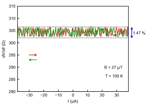
To check whether the asymmetry in switching current is due to contact related issues, normal state is measured at different magnetic fields for up and down directional sweep of biasing current. Fig. S9 shows the response at a particular . It is clear from Fig. S9 that for up and down direction biasing current sweep normal state differential resistance is not different within the noise limit. The asymmetry of switching current that we observe is not related to contacts.
S11 Thicknesses and perpendicular B range for asymmetry tunability of the twisted devices
We have performed AFM measurements to get the thicknesses of the individual BSCCO flakes. These measurements are done after we complete the electrical measurements on these devices. Thickness data are tabulated below. In the table, we also provide the areas of the twisted junctions for all the devices along with the perpendicular range over which we observe the switching current asymmetry tuning. The range for tuning asymmetry is always smaller for the twisted devices than the and twisted devices.
| Device No. | Twist angle | Top flake thickness | Bottom flake thickness | Junction area (µm2) | range for asymmetry tunability (µT) |
| D1 | 45° | 24 nm | 13 nm | 340 | 20 |
| D2 | 0° | 50 nm | 30 nm | 290 | 300 |
| D3 | 45° | 60 nm | 30 nm | 154 | not measured |
| D4 | 0° | 32 nm | 24 nm | 367 | not measured |
| D5 | 22° | 65 nm | 25 nm | 450 | 300 |
| D6 | 45° | 45 nm | 34 nm | 1387 | 30 |
| D7 | 45° | 60 nm | 30 nm | 248 | 20 |
| D8 | 0° | 150 nm | 40 nm | 720 | 250 |
| D9 | 0° | 55 nm | 18 nm | 234 | 350 |
| D10 | 22° | 90 nm | 20 nm | 187 | 400 |
S12 Measurement setup for field dependent asymmetry
We have measured our devices in two different setups. Setup 1 is a closed-cycle cryogenic probe station (Lakeshore CRX-6.5 K) with a homemade electromagnet. Setup 2 is a wet cryostat (Oxford instrument) with an inbuilt superconducting magnet.
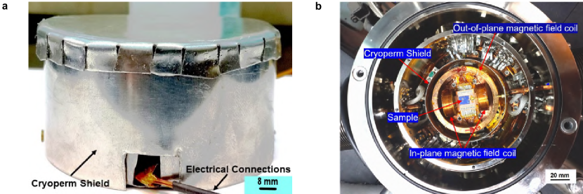
The homemade electromagnetic coil in setup 1 is a solenoidal coil made up of 1200 turns of copper wire (diameter 0.2 mm) with an inner radius of 19.5 mm, an outer radius of 24.5 mm, and a width of 12 mm. The fabricated devices are mounted at the center of this homemade solenoid coil. The direction of the generated magnetic field is perpendicular to the plane of the BSCCO flake. We also installed coils for generating an in-plane magnetic field. The electromagnet along with the device is then covered from all sides using a cryoperm magnetic shield, which prevents any stray magnetic field from affecting the device. Fig. S10a shows the cryoperm magnetic shield. We have modified the inside design of a closed-cycle cryogenic probe station (Lakeshore CRX-6.5 K) to accommodate the entire assembly of the coil and the shield, as shown in Fig. S10b. The 45° twisted device presented in the main manuscript is measured in this homemade electromagnetic setup (setup 1) inside the probe station.
Setup 2 is the Oxford instrument wet cryostat where an inbuilt superconducting magnet generates the magnetic field perpendicular to the device plane. This setup has no magnetic shielding. The data of the 0° and 22° twisted devices, presented in the main manuscript, are taken in this setup 2.
To accurately determine the actual magnetic fields at the position of the device, we calibrate the magnetic fields in both setups. The calibration is done by the Bartington Mag-01H single-axis fluxgate magnetometer with Mag G probe DR2909 sensor. The sensor has a measuring range of 0 to 2 mT with a sensitivity of 1 nT. We place the sensor at the position of the device, perpendicular to the device plane. By sending a current through a Keithley source meter (model no. 2635A) we measured the field generated by the electromagnets.
S13 Temperature dependence of and
Fig. S11a, b show temperature dependent I-V for both directions of bias current sweep for the twisted device (D1). The switching currents at different temperatures for positive bias () are shown by open blue circles in Fig. S11a. The switching currents at different temperatures for negative bias () are shown by open orange circles in Fig. S11a. Fig. S11c shows temperature dependence of and simultaneously. This is data from the same device (D1) as Fig. 1 and Fig. 2 in the main manuscript. The data has been taken with zero current in the magnet coil (for producing a magnetic field in the setup). But as we mentioned in our manuscript (Caption in Fig. 2), there is a field offset of µT in our measurement setup which accounts for the asymmetry between and even at zero externally applied .
S14 Fraunhofer modulation of switching current – a signature of Josephson tunneling
A strong signature of a Josephson junction is the Fraunhofer pattern-like modulation of its critical current in a magnetic field applied perpendicular to the Josephson current (). For our -axis twisted BSCCO devices, this will happen when the applied will be in-plane (), as shown in Fig. S12a. We observe a Fraunhofer-like pattern of the smallest switching current (attributed to the artificial Josephson junction at the interface) with in-plane as shown in Fig. S12b at 50 K for a twisted device (D5). This shows the Josephson coupling between the two twisted layers of BSCCO and the Josephson junction is in the short junction limit (Josephson penetration length ; is the width of the Josephson junction). We observe asymmetry between and in this configuration as well. However, we attribute this observed asymmetry to the contribution of the out-of-plane component of applied because of a small tilt between the sample plane and direction. It is very hard to perfectly align the sample plane with the in-plane and avoid any out-of-plane component of it. As we see in Fig. S13e and f (data from the same device as in Fig. S12) the asymmetry arises with very small out-of-plane B ( 100 µT). So even a misalignment of in-plane by a few degrees will have a significant out-of-plane component. Fig. S12d, e show distributions for 10000 switching events for and at different marked by red and grey star and hexagon in Fig. S12b. The shapes of the switching distributions for and are asymmetric.

S15 In-plane vs. out-of-plane magnetic field dependent switching current asymmetry
Fig. S13 summarizes the different behaviour of switching current asymmetry in devices with different twist angles in two different configurations of externally applied magnetic field (). In out-of-plane (Fig. S13b), we observe large asymmetry in switching current for all twist angles (Fig. S13d, f, h). When we apply the same range of in-plane (Fig. S13a), we do not see a significant asymmetry in switching current (Fig. S13c, e, g).

S16 Control experiment in pristine BSCCO without involving junction
In Fig. S14, we present a control experiment in extended pristine BSCCO away from the twisted junction. This control experiment is similar to the control experiment provided in Extended Data Fig. 2 except that the bias current now flows only in the pristine BSCCO and not through the junction. Fig. S14a shows the measurement protocol for switching current asymmetry in the pristine BSCCO. Fig. S14b shows simultaneously the asymmetry arising from the junction and pristine BSCCO. Similar to the data in Extended Data Fig. 2, we observe very small asymmetry () in pristine BSCCO. This control experiment along with the one provided in Extended Data Fig. 2 show that there is a negligible asymmetry in the pristine BSCCO flake in presence of an out-of-plane B.
S17 Theoretical scenario
S17.1 Origin of diode behavior
We provide additional background on the theoretical scenario sketched in the main text. Due to its layered structure, BSCCO has strongly asymmetric magnetic response, with m much smaller than the width of the sample and m much larger than the height of the flakes. The magnetic field applied along the -axis will thus enter in stacks of pancake vortices. The AJJ realizes an extended Josephson contact (in the -plane) with Josephson current
| (S1) |
where denotes the gauge-invariant phase difference across the junction as a function of position. Equation (S1) assumes a spatially independent coupling strength (and hence ) across the contact as well as weak coupling so that the Josephson current is sinusoidal in the phase difference.
In general, the phase difference depends on the externally applied field as well as self fields generated by the Josephson current. We estimate that self-fields are negligible since the junction width is smaller than the Josephson penetration depth m (with sample thickness , flux quantum , and critical current density taken at a twist angle of ). This is consistent with the observed Fraunhofer-like interference at large in-plane fields (Fig. S12). Thus, the phase difference is controlled by the applied magnetic field and remains uniform across the junction as long as the field is pointing along the -axis only. This is true even if the flux enters in -axis-aligned vortex stacks, for which the phase configurations of top and bottom flakes would be identical.

The phase difference is no longer spatially uniform when the vortex stacks are not passing vertically through the entire sample. At the AJJ, the Josephson coupling and hence the coupling between pancake vortices is weakest. Moreover, top and bottom flakes have uncorrelated defect contributions, favoring pinning of vortex stacks at different sample locations. As a result, magnetic flux must exit at the AJJ within the -plane or connect between vortex stacks of the top and bottom layers [42, 43]. (Effectively, the latter situation would correspond to the formation of a Josephson vortex at the AJJ, although it should be kept in mind that the flux is only weakly concentrated at the interface as the height of the flakes is small compared to .) This results in a spatially dependent phase difference and thus Fraunhofer-like interference [see Eq. (S1)], both due to the incongruent phase configurations associated with the vortices in top and bottom flakes and due to the magnetic field along the -plane.
Josephson diode behavior appears due to self-field effects or current-induced changes in the vortex configurations (Magnus force). The sample geometry is such that the bias current is effectively flowing within the -plane. Thus, self fields contribute to the flux penetrating the junction parallel to the -plane. Moreover, the bias current exerts Magnus forces on the vortex stacks in the upper and lower flake. Importantly, both the self field and the Magnus force change sign with the direction of current bias and thus affect the Fraunhofer-like interference asymmetrically. The changes in the interference pattern can be substantial when the vortex configuration changes. In contrast, we estimate below (see Sec. S17.3) that self-field effects tend to be smaller than the observed asymmetries, a fact which is consistent with the large Josephson length. We thus conclude that the diode effect is dominated by vortex rearrangements in the presence of Magnus forces exerted by the bias current.
As described in the main text, this scenario is consistent with the principal experimental observations. In the next section, we give more details on the switching-current distributions.
S17.2 Switching current distribution
The switching dynamics of the Josephson diode can be described within the model of a resistively and capacitively shunted Josephson junction (RCSJ model), see, e.g., [39, 41]. Within this model, the phase dynamics in the presence of a bias current is described by the Langevin equation
| (S2) |
for the phase difference . Here, is the junction capacitance, accounts for quasiparticle dissipation, is the associated Johnson-Nyquist noise with correlator , and denotes the current-phase relation. The Johnson-Nyquist noise induces a distribution of switching currents . The average is reduced relative to the critical current (maximum of current-phase relation) and the variance of the distribution is controlled by (the effective) temperature, (see Sec. S17.4 below). Equation (S1) gives a current-phase relation
| (S3) |
where is the average phase difference across the junction (i.e., a constant offset of ). According to the discussion in the previous section, the critical current depends on the applied magnetic field as well as the bias current .
We note that for K, one estimates A. This is close to, but smaller than the experimentally observed values. Additional nonthermal noise contributions to the Langevin current increase the width, but cannot explain the observed multiple humps and asymmetries in the width of the switching current distribution. Both of these can be understood as a consequence of multistabilities of the vortex configurations at fixed and . Multihump distributions reflect multistability of vortex configuations with sufficiently different critical currents. Asymmetries reflect the distinct (multistabilities of the) vortex configurations for the two bias corrections, which also underlie the observed asymmetry of the average switching current.
Asymmetric widths of the switching current distributions can also appear as a consequence of non-sinusoidal current-phase relations, see Sec. S17.4. An asymmetry arises for washboard potentials in which the minimum is located asymmetrically between neighboring maxima. A similar effect can occur as a result of self fields, which effectively act as a current-induced phase offset of the current-phase relationship. While this can in principle contribute to asymmetric widths, this mechanism cannot explain the multi-hump distributions and is presumably weak along with higher harmonics of the current-phase relationship and/or the self-field effects.
S17.3 Self-field effects due to the bias current
We estimate the asymmetry due to self-field effects of the bias current. The sample geometry is such that the bias current effectively flows within the -plane. A thin-plate conductor in the -plane (thickness ) with a uniform current density flowing in the -direction produces a magnetic field
| (S4) |
in the -direction, which is uniform above and below the plate, with opposite signs. Viewing the entire sample as such a thin plate conductor (on scales large compared to its thickness), we then find that it induces a field sufficiently far from the sample plane, where is the sample width in the -direction and is the current bias.
We are interested in the induced field in the junction region. For the purpose of an estimate, we simplify considerations by assuming that the system and the magnetic-field configuration is uniform in the -direction. Then, the Josephson current in the -direction can be expressed as
| (S5) |
where we assume that the junction extends between and in the -direction (i.e., is the phase difference at the center of the junction). Here, denotes the flux penetrating the junction in the -direction between and . Due to the inhomogeneous field distribution originating from the vortex configuration, this will usually not be a linear function of .
We want to compute the currents in the upper and lower electrodes. We first note that the currents are approximately uniform in the -direction, since the thickness of the flakes is small compared to the London penentration depth. The cross section at any must be passed by the current . Correspondingly, we write the current in the -direction in the lower flake as and in the upper flake as . Continuity implies
| (S6) |
This should be supplemented by the boundary conditions and .
We can now obtain
| (S7) |
with the condition that
| (S8) |
Note that this condition basically determines the phase difference across the junction. We enclose, say, the lower flake by an Amperian loop to obtain the induced magnetic field within the junction. This gives
| (S9) |
This field in turn affects the phase difference, so that we should use
| (S10) |
Here, the effective thickness is of the order of the thickness of the sample in the -direction.
Estimating the contribution of the induced field to the flux penetrating the junction (total sample thickness of nm, a width of 20m, and bias current A), we estimate , which would correspond to an asymmetry of the order of a percent, considerably smaller than observed in the experiment.
S17.4 Width of switching-current distribution
We derive the switching-current distribution accounting for general current-phase relationships. Our calculation extends the calculation of the average switching current presented in Ref. [41] to the distribution function. Our notation, including the definition of dimensionless units, follows this reference.
The (dimensionless) switching rate is given by [54, 41]
| (S11) |
where is the barrier height, is the energy dissipated along the separatrix motion, and is the plasma frequency. All quantities, including temperature , are in dimensionless units, see [41]. We consider a linear ramp of the bias current from zero (ramp rate ),
| (S12) |
The sign indicates the direction of the ramp. We denote by the probability that the system is still in the trapped state at (dimensionless) time . This probability obeys the rate equation
| (S13) |
The escape rate out of the trapped state is time dependent, since the barrier height is a function of the bias current . Solving for with initial condition gives
| (S14) |
We use Eq. (S12) to replace time by current,
| (S15) |
The switching rate depends exponentially on the barrier height , which decreases with bias current. At low temperatures, the integral in the exponent is thus dominated by the upper limit. This gives
| (S16) |
The switching probability can be extracted from as
| (S17) |
which yields
| (S18) |
We expect to be a sharply peaked function, which we approximate as a Gaussian.
This is implemented by writing
| (S19) |
with
| (S20) |
We expand about its minimum at ,
| (S21) |
We have
| (S22) |
Thus, the condition yields
| (S23) |
and
| (S24) |
Furthermore, we have
| (S25) | |||||
We denote the phase differences at which the tilted washboard potential becomes maximal (minimal) as (). Using
| (S26) | |||||
we have quite generally
| (S27) |
We then find
| (S28) |
Here, we have fixed the numerical prefactor by normalization. We have added a superscript to to , since the relevant maximum depends on current direction. Similarly, we indicated the dependence of the average switching current on the direction of the bias current. Finally reverting to dimensional variables (written in capitals), we obtain
| (S29) |
As long as the Langevin fluctuations reduce the average switching current significantly below the critical current, the tilt of the washboard potential is small and we can approximate . This gives the estimate for the width of the switching current quoted above. For general tilts, this provides a lower limit to the width of the switching current distribution, which may moreover become asymmetric (but not multi-humped) for asymmetric .