Characteristics of quantum emitters in hexagonal boron nitride suitable for integration with nanophotonic platforms
Abstract
Single photon emitters in two-dimensional (2D) hexagonal boron nitride (hBN) are promising solid-state quantum emitters for photonic applications and quantum networks. Despite their favorable properties, it has so far remained elusive to determine the origin of these emitters. We focus on two different kinds of hBN samples that particularly lend themselves for integration with nanophotonic devices, multilayer nanoflakes produced by liquid phase exfoliation (LPE) and a layer engineered sample from hBN grown by chemical vapour deposition (CVD). We investigate their inherent defects and fit their emission properties to computationally simulated optical properties of likely carbon-related defects. Thereby we are able to narrow down the origin of emitters found in these samples and find that the defect fits our spectral data best. In addition, we demonstrate a scalable way of coupling LPE hBN to optical nanofibers that are directly connected to optical fibers. Our work brings us one step closer to specifying the origin of hBN’s promising quantum emitters and sheds more light onto the characteristics of emitters in samples that are particularly suited for integration with nanophotonics. This knowledge will prove invaluable for novel nanophotonic platforms and may contribute towards the employment of hBN for future quantum technologies.
1 Introduction
Quantum emitters in two-dimensional (2D) materials are gaining increasing interest due to their remarkable properties[1, 2, 4, 5, 6]. Particularly quantum emitters in hexagonal boron nitride (hBN) have been shown to be very stable over a wide temperature range [7, 8, 9], have bright emission into the zero-phonon line (ZPL) even at room temperature with Debye-Waller (DW) factors exceeding 0.8 [1] and their transition frequency can be tuned via the Stark effect[10]. Some quantum emitters in hBN may even exhibit lifetime limited emission at room temperature [11, 12], which has not been seen in any other solid-state quantum emitter so far. In addition, the 2D geometry of the host material particularly lends itself for the integration with nanophotonic devices. However, although these quantum emitters particularly around transition energies of 2.2 eV exhibit many advantageous properties, much remains unknown about their origin. A key reason is that to date direct correlation of atomic defect structure with quantum emission properties has experimentally not been achievable yet for these type of defects [13], and thus indirect methods for correlating atomic structure and quantum emission are commonly used.
Here, we aim to shed more light on these quantum emitters by comparing their experimental emission properties to those of computationally simulated defects and by comparing the properties of two different kinds of samples that are ideal for integration with different nanophotonic platforms. To fully exploit all of the advantages of solid-state emitters as single photon sources or constituents of photonic quantum networks and implement scalable devices, near-field coupling of the emission to waveguides or microcavities is key. Therefore we focus on two different kinds of samples, small hBN flakes produced by liquid-phase exfoliation (LPE) and layer-engineered hBN films grown by chemical vapour deposition (CVD). Due to their small size, LPE hBN nanoflakes in liquid suspension, are an ideal sample for integration with free-standing nanophotonic waveguides, such as optical nanofibers [14], that are naturally integrated with any optical fiber network. Previous work has demonstrated the deterministic placement of quantum emitting hBN flakes onto an optical nanofiber using a lift-off/transfer technique via a micromanipulator[15]. Although very precise, micromanipulator-based deterministic placement can be hard to scale and thus here, we present an alternative integration pathway where LPE hBN flakes are initially dispersed in a liquid suspension and then transferred to the fiber using a simple “drop-touch” approach (Fig.1)[14, 16]. The CVD grown hBN film sample on the other hand is designed to work for planar waveguide chips and photonic circuits. Here the focus lies in obtaining high quality thin hBN films. To shield the emitters from photobleaching, one layer of CVD hBN with quantum emitters is shielded from the environment by only two layers of CVD hBN that do not exhibit any emitters. More details on the production can be found in [17]. Such a layer-engineering approach allows for more control over the position of the emitters and as the thickness of the sample is only three atomic layers, light scattering by the host crystal is negligible. For both hBN samples we study the properties of the most abundant single photon emitters found. We have made sure that their photoluminescence (PL) signatures correspond to the most abundant type found in the respective substrates also in previous literature [18, 1, 19, 20, 21, 22, 23]. These defects have been found to occur inherently in these types of samples even without any post-processing.
In this report, we study the single photon emitting inherent defects in these two nanophotonically beneficial sample types by comparison of experimental and computationally simulated emission properties with respect to likely carbon-related defects. Thereby we are able to narrow down the possible origin of these emitters, and find that the defect fits our experimental spectral data for both sample best.
2 Results
2.1 hBN quantum emitters coupled to the guided modes of an optical nanofiber
To demonstrate that the LPE sample is ideal for integration with free-standing waveguides, we employ an optical nanofiber interface for excitation and detection of the quantum emitter.
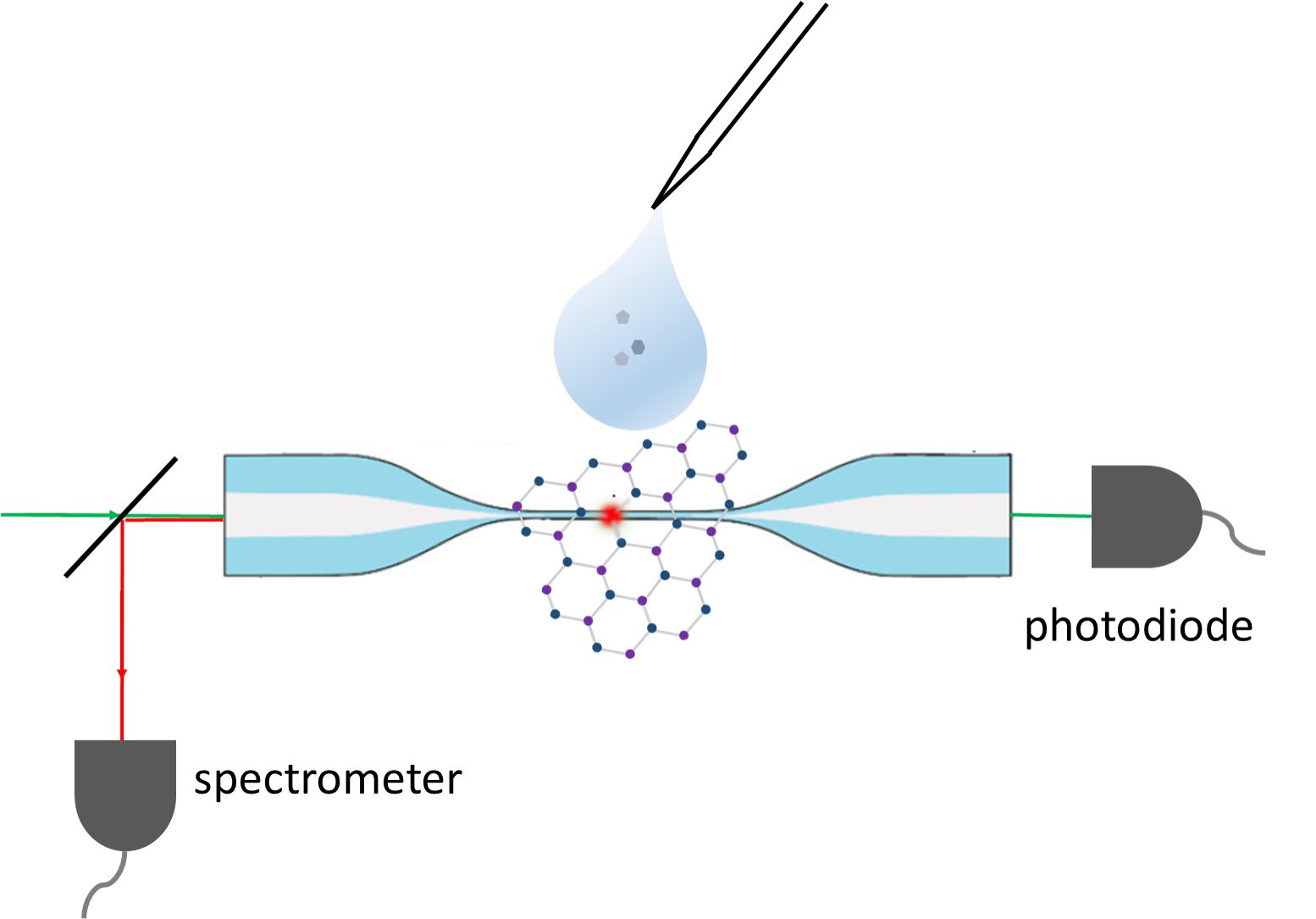
Optical nanofibers offer a convenient way for near-field coupling of quantum emission. By placing solid-state emitters on the surface of these nanophotonic devices, coupling efficiencies of over 20 % can be achieved [14, 24, 25] and when combined with cavity structures [26], Purcell factors of more than 15 can be reached [27, 28]. We employ optical nanofibers that are tapered by a custom made heat-and-pull process [29]. A nanofiber waist of 320 nm ensures that for an excitation wavelength of 570 nm, only the fundamental HE11 mode is guided. Emission into a single mode is a pre-requisite for many applications of future quantum technologies and is also needed for fundamental experiments in quantum optics.
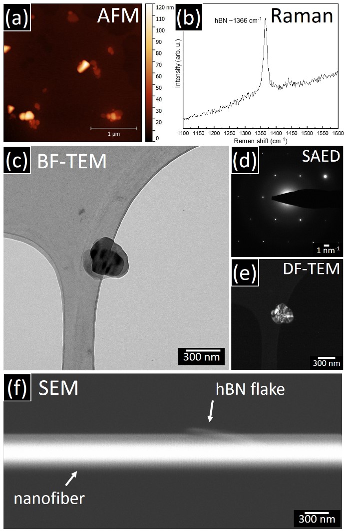
To interface the hBN quantum emitters with the nanofiber-guided light field, we use LPE hBN nanoflakes that are suspended in a water:ethanol mixture. To estimate the hBN flakes’ lateral size and thickness distributions and confirm their structure, a droplet of the solution is dropcast onto a SiO2 covered Si wafer or lacy carbon transmission electron microscopy (TEM) grid and atomic force microscopy (AFM), Raman spectroscopy and TEM in bright-field (BF) and dark-field (DF) modes and selected area electron diffraction (SAED) are used. The AFM topography data in Fig. 2a confirms that the hBN flakes exhibit "platelet"-type morphology. Upon drying from a droplet on the flat SiO2 covered Si wafer substrate often several individual platelets re-agglomerate into stacks. From AFM height profiles of individual flakes we estimate lateral platelet sizes to range from 90 nm to 300 nm with a mean of 160 nm and vertical platelet heights from 10 nm to 110 nm with a mean of 28 nm. Considering that a hBN monolayer has a height of 0.34 nm [30] the observed flakes are few- to multi-layered hBN, which has been shown to be beneficial concerning the stability of the emitters [1]. Calculating the thickness:length ratio of the platelets gives an average of 0.16, confirming that we are indeed using flat hBN platelets for our experiments. The Raman spectrum in Fig. 2b confirms that the platelets are hBN via its characteristic Raman signal at 1366 cm-1 [30]. The BF-TEM in Fig. 2c shows a single hBN platelet deposited onto a lacey carbon strand. The corresponding SAED pattern in Fig. 2d confirms that this hBN platelet is a hBN single crystal [31]. The DF-TEM in Fig. 2e however indicates via contrast variation that within the hBN single crystal stacking faults exist [32]. Notably, both on flat SiO2 covered Si wafer and on more curved lacey carbon supports all observed hBN flakes are stuck to the support in planar configuration, suggesting that a similar planar hBN orientation on the nanofiber surface should be feasible.
The hBN flakes are placed on the nanofiber by a “drop-touch” method. Hereby a drop from a syringe of hBN suspension is put into contact with the nanofiber surface using a micro-translation stage and then moved away again, until a flake adheres to the nanofiber surface. During this process, the light of a dye laser at 570 nm is coupled into the optical fiber and the backscattered fluorescence is measured using a spectrometer. Reflected laser light is filtered out by a longpass filter for 610 nm. If an hBN flake containing quantum emitters has been deposited on the nanofiber in this process, a fluorescence from the quantum emitters can be seen in the fluorescence spectrum. If not, the process can be repeated. This process of deposition of nanoparticles on a nanofiber is simple and scaleable. To ensure that the nanofiber does not become coated with flakes that don’t host emitters, it is advantageous if most flakes do contain an emitter. Successful deposition of hBN flakes can also be visualised using scanning electron microscopy (SEM), as shown in Fig. 2f, which shows deposition results after “drop-touch” of hBN suspension on a nanofiber. Notably the object identified as an LPE hBN flake rests in a planar configuration on the nanofiber, consistent with the characterisation data for the other substrates in Fig. 2a-e.
2.2 Layer-engineered hBN
For integration with chip based structures, a thin, flat structure is more advantageous. For this purpose a stack of three CVD hBN layers is engineered [17], where only the central layer hosts single photon emitters and the two outer layers function as a protection against bleaching of the emitters (3). More details on the sample can be found in the Methods section and in [17].
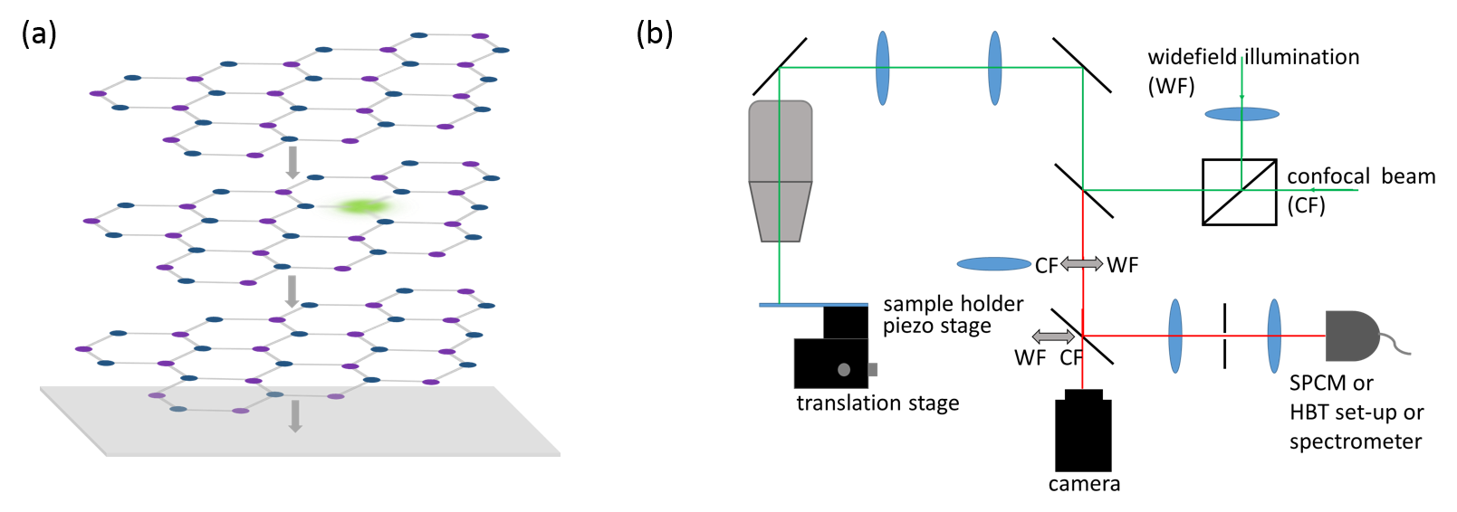
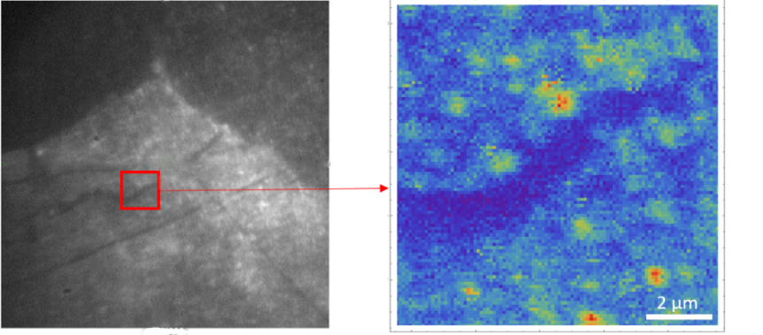
We study this trilayer sample using a homebuilt confocal microscope with a diode laser at 532 nm. The microscope can either function in confocal or widefield mode, an example of which can be seen in Fig. 4.
2.3 Second-order fluorescence correlation measurements
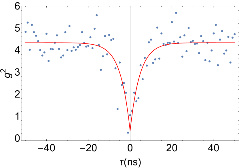
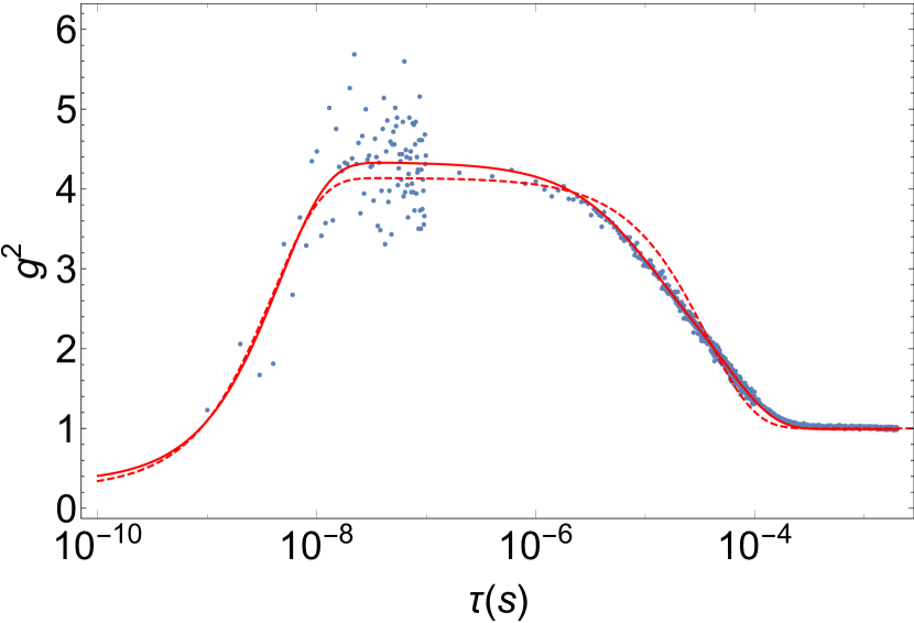
To verify that the investigated emitters in both samples are indeed single photon emitters and to obtain more information on their internal level structure, we have performed second-order intensity correlation measurements on both types of emitters and correlated the coincidences long enough so that the normalised measurement reaches a value of which indicates that the system is in equilibrium from that time onwards. These measurements give an indication if more levels are involved in the decay process and if their contribution can be significant. At , a dip that goes below 0.5 indicates that the collected light predominantly stems from a single photon emitter. The correlation measurements of the LPE sample and the CVD sample are displayed for long and short times in Fig. 5 and Fig. 6, respectively.
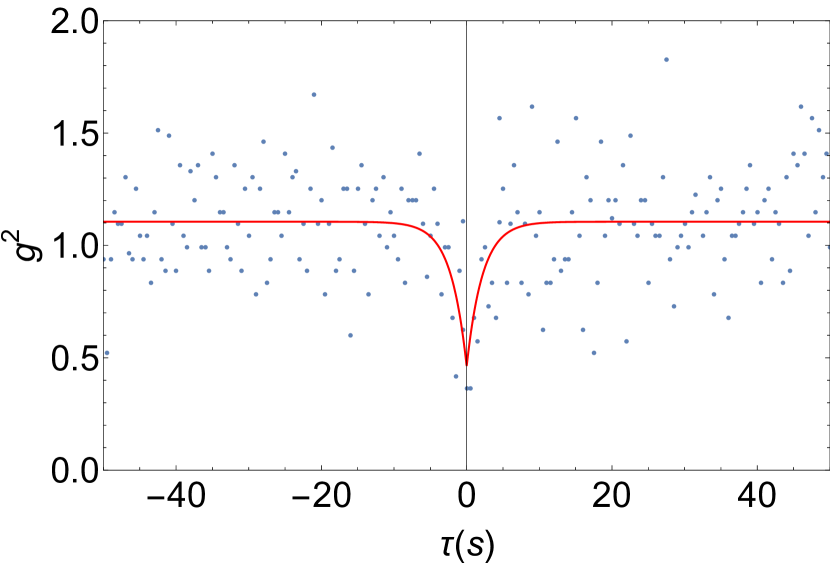
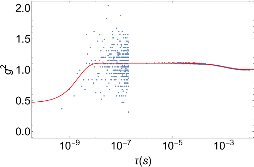
To fit the correlation measurements, we generally assume a four-level model, where a laser excites the emitters off-resonantly from the ground electronic state 1 to an excited state 2. The laser is blue detuned from this transition and thus the excess energy is carried away by phonons. As this happens on a picosecond scale, rate equations are sufficient to describe the dynamics of the system. From state 2, the emitter can then either decay back to level 1 by emitting a photon or decay to one of two metastable states (states 3 and 4) via intersystem crossing. From either of these metastable states, the emitter then decays back to the ground state and can be re-excited. The corresponding rate equations are explicitly given in the supplementary information (eqn. 1). In addition, the data has also been fit to a simple model of three exponential decays , where represents the lifetime of the excited state and and are the time constants for the two metastable states. represents the fraction of the signal compared to the total count rate obtained from the sample that may include some Poissonian background . In the case of the CVD grown sample, the bunching effect is less pronounced and measurements at only one power cannot be used to unambiguously determine all the rates. As the defects in the layer-engineered sample photobleach more easily, g2 measurements which require laser irradiation of the defect of at least an hour could not be performed at different excitation powers. Hence, for the CVD sample, we only fit the simple exponential model with one metastable state.
In table 1, a summary of the most important fit parameters for the two samples are given. The detailed results of both the rate equation and simple exponential model are found in the supplementary information (Tab. 1).
| LPE sample (rate eqn. model) | LPE sample (exp. model) | CVD sample (exp. model) | |
|---|---|---|---|
| fit parameter | parameter value | parameter value | parameter value |
| - | |||
For both samples, the ratio of signal to background from the spectrum and that obtained from the fit agree well and further confirm a indicating single photon emission. For the LPE sample, a smaller value for is observed, which is not surprising as scattering from the nanofiber adds to the background. The intensity correlation measurements from the fluorescence of both samples show a similar radiative lifetime of the electronic excited state. The defect from the LPE sample shows a higher bunching value for similar excitation powers used and faster decay from the metastable state. For similar excitation intensities used, this indicates either a different type of emitter, a better overlap between excitation field and dipole or a higher intersystem crossing rate due to the difference in detuning from the excitation laser with respect to the ZPL. The latter has also been observed previously [18] and the more efficient optical pumping also ties in with the observed higher bunching effect and with power-dependent intersystem crossing as observed in other solid-state systems [33]. For the LPE sample, we compare the fits to a 3-level and 4-level rate equation model and clearly find that for this defect four levels and hence the existence of at least two resolvable metastable states is required to yield a good fit (Fig. 5). While the simple exponential model fits the data equally well, the two timeconstants do not directly correspond to the lifetimes of the two metastable states but are underestimated in this case, since this simple model does not take the rates into account that correspond to transfer from the electronic excited states to these metastable states. For the CVD sample, the bunching effect is less pronounced and thus only the existence of one metastable level can be unambiguously resolved. Nevertheless it is found that at least one metastable state is needed to accurately describe the system.
2.4 Comparison of experimental and theoretical spectra
To gain more information on the types of defect responsible for the single photon emission in these two sample types, we measure their spectral emission characteristics. When exciting the single photon emitters with energies higher than the resonance electronic transition, the PL spectrum consists of both the ZPL and the phonon sideband (PSB). Such a spectrum therefore yields important information on the electronic and phononic transitions of the defect and hence its potential energy surface. The expected transitions can also be theoretically simulated and hence we can compare our experimental results to those of simulated defects in hBN.
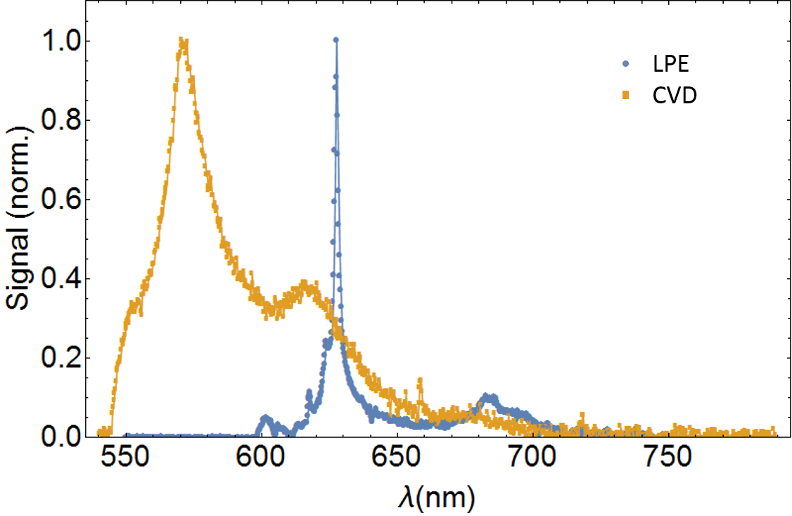
In Fig. 7, a spectrum of a nanofiber-coupled hBN quantum emitter in an LPE sample and a spectrum of a quantum emitter in CVD grown hBN are shown. The LPE sample shows a sharp but asymmetric peak at 628 nm corresponding to the ZPL of the emitters and a PSB that clearly features a double peak. When fit to three Lorentzian functions, the ZPL shows a width of nm (FWHM). This is in agreement with previous values obtained in literature using the same fitting procedure [34, 22, 20] for LPE samples and therefore underpins further that LPE hBN without post-processing predominantly features this type of defect.
For the spectra of individual quantum emitters in layer-engineered CVD hBN, we observe a broader first peak of nm (FWHM), when fit to a Lorentzian. This broader linewidth and ZPLs of these emitters pre-dominently found between 570-590 nm, have also been reported in previous literature for standard CVD growth conditions [18, 35, 36, 37].
Theoretically a number of possible candidates for single photon emitters in hBN has been suggested [17, 38] from simple vacancies [39] to carbon-based defects [40], to dangling bonds [41]. There are conditions that these defects have to meet for them to be likely to be the origin of single photon emitters in hBN in the visible range.
It is required that at least two states of the defect are found within the bandgap of hBN that are neither both fully occupied nor both completely empty and that the calculated PL spectrum features a sharp and strong ZPL with a phonon sideband peak of 160-180 meV from the ZPL as found experimentally. Density functional theory (DFT) calculations are usually not very exact concerning the absolute transition energy and thus the results of the absolute ZPL energy are not trustworthy enough to pick the correct origin of the emitter. However, the spacing between different transitions is more reliably and can be used to identify possible candidates.
Considering vacancies where only one atom is missing from the lattice, the defect has recently been identified as being likely responsible for a very broad emission at 850 nm [42, 4, 43] and hence we exclude it as a likely candidate for the ones found in the visible range that feature a narrow distinct ZPL. Although not found experimentally, calculations for the defect have shown that this defect is also likely to feature a very broad and dominant PSB [44] and thus we do not consider this defect further here.

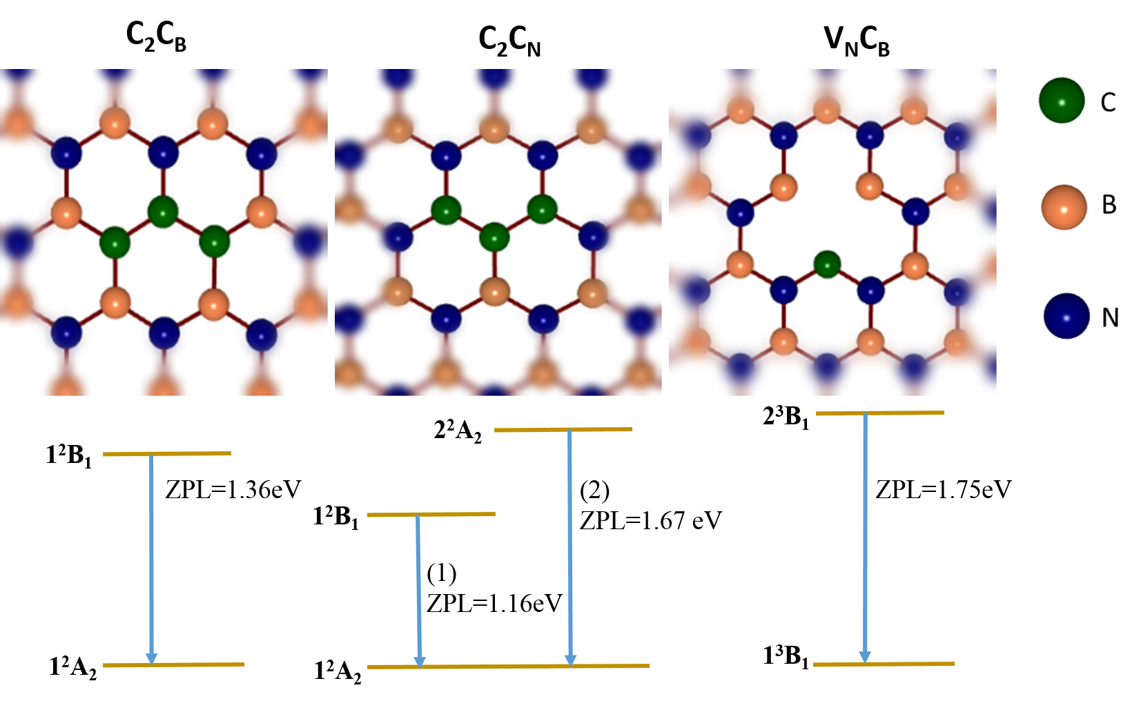
As here we are interested in emitters that are inherently found in the material without complex post-processing we also have to consider which defects are favourable concerning their formation energy. Recently it has been suggested that carbon plays a crucial role in emitter formation [40] and it has been observed that a deliberate carbon atmosphere during the growth process indeed increases the density of emitters in CVD grown hBN [45]. Although it has been calculated [44] that the formation energy of a carbon atom substituting a boron or nitrogen atom in pristine hBN is too high to occur for thermal mechanisms, the formation energy for a carbon impurity taking a place of a pre-exisiting vacancy is very favorable. While the carbon monomers and have been shown to be unsuitable as candidates for single photon emitters , the carbon trimers and (where stands for ) are likely candidates. The formation energy needed for these impurities to fill a vacancy are found to be -9.12 eV and -5.6 eV [44], for the and , respectively and thus this process is very favorable in both cases.
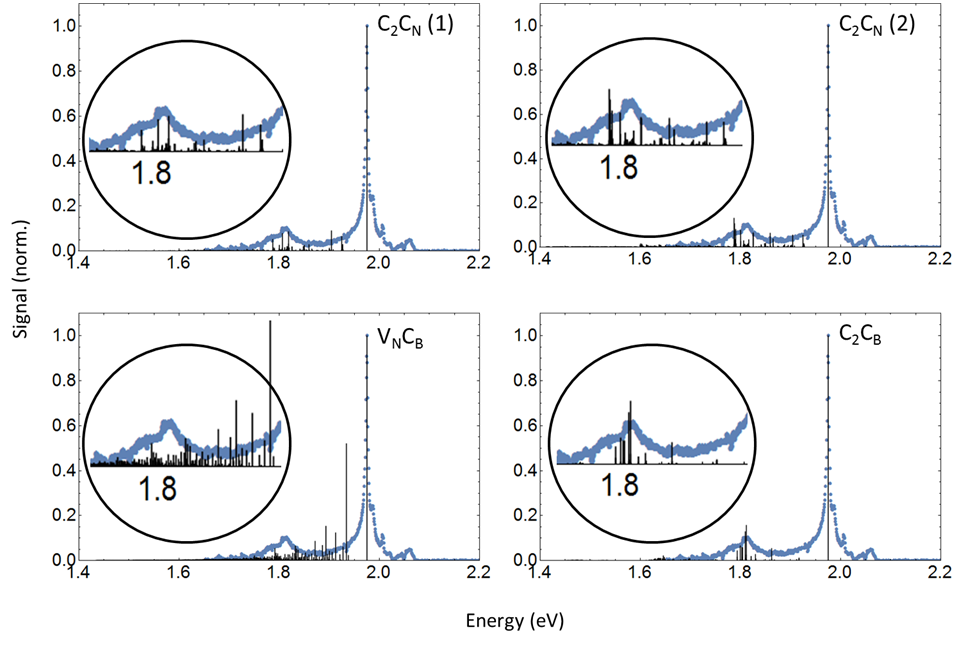
Therefore, we focus on three different possible defects, the , the and the defect. The schematic geometrical structure of the three defects in symmetry is shown in Fig. 8. For our calculations of the PL spectra of these three defects, we consider ZPL transitions that have energies between 1-3 eV as uncertainties on the order of 0.5-1 eV are not uncommon for absolute results of the transition energies from DFT simulations. The relevant transitions are displayed in Fig. 8. For two possible transitions exist that meet the above criteria and these are labelled (1) and (2) throughout the manuscript corresponding to the and the transition, respectively (Fig. 8). The planar configuration of the dipole for ground and excited state is the most stable one for all cases except for the excited state of , where the carbon atom of the defect relaxes out of plane. The out-of-plane configuration is stable compared to the planar configuration and differs by 0.23 eV for monolayer hBN, while the energies differ by 0.036 eV in a trilayer hBN with a defect embedded in the central hBN layer. The analysis of phonon modes for and reveal that the bulk like modes have a dominant contribution for while for and the localized stretch mode of the three carbon atoms has a dominant contribution to the PSB. This is in agreement with previous studies[46, 44]. Figure 9 shows the PL spectrum of a defect in LPE hBN and the zero-phonon transitions and phonon modes of the three different defects as given by our simulations. Here, the ZPL of the simulated results has been shifted to match the energy of the experiment. This is valid, as DFT calculations are not accurate enough to determine the absolute transition energy but can be trusted to estimate the relative transition energies of the different modes involved. The relative intensity of the ZPL compared to the total PL intensity is described by the DW factor and is also simulated with our calculations. The values for the different defects are found in table 2.
| defect | simulated DW factor |
|---|---|
| 0.37 | |
| 0.26 | |
| 0.22 | |
| 0.47 |
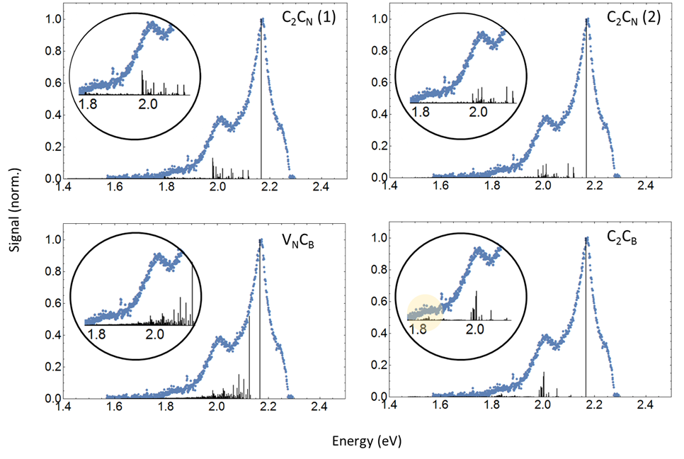
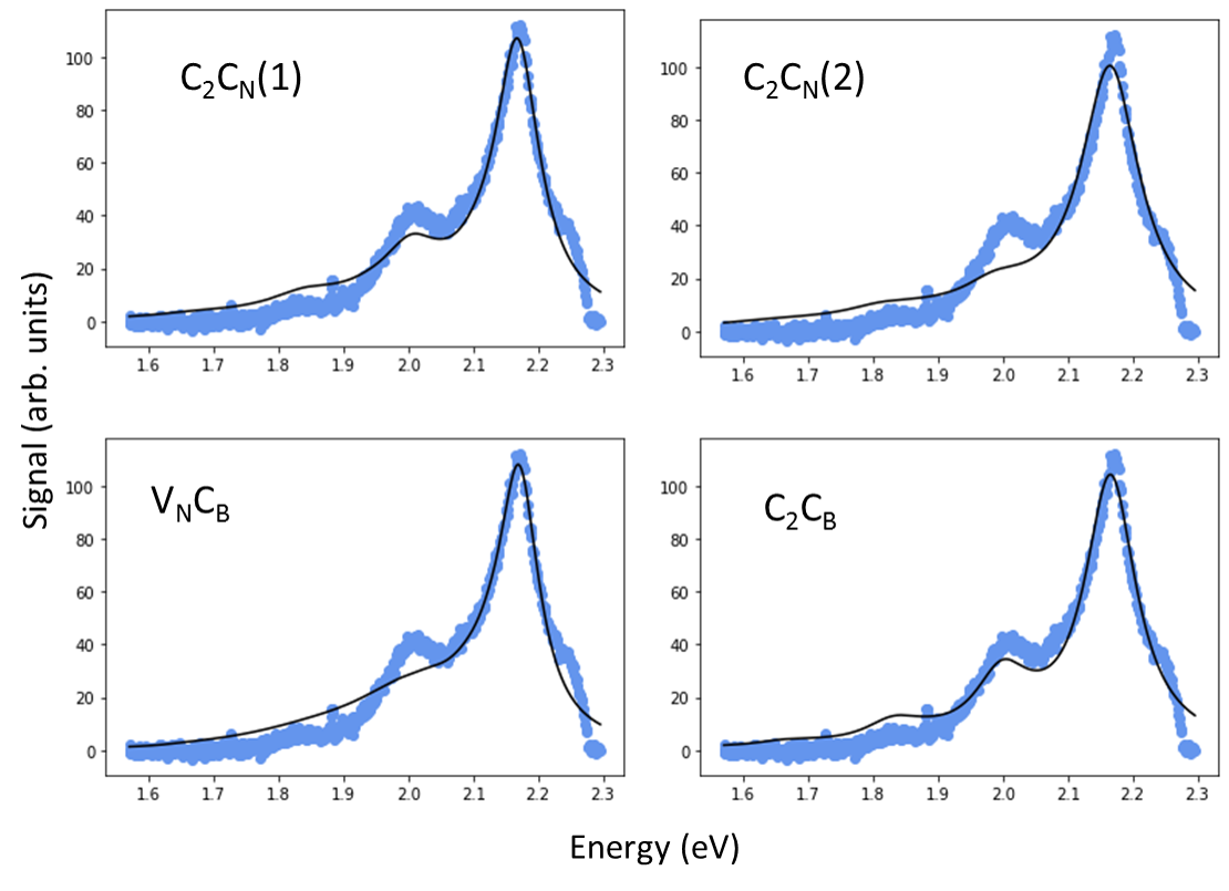
Comparing the experimentally measured spectrum to the expected modes shows that the results for the defect match best, especially when looking closely at the phonon sideband (insets in Fig. 9). All other defects have phonon transitions that should lead to additional peaks in the experimental data. Fig. 10 shows the comparison of simulations and the PL spectrum of an emitter in the CVD sample. At first sight both, the defect (second transition) and the defect seem to match the measured data. However looking more closely one finds that no defect apart from the has a significant phonon contributions at 1.8 eV leading to the small third bump in the experimental spectrum (highlighted in Fig. 10) . Thus, surprisingly, based on these observations, the is the most likely candidate as the inherent single photon emitter in both types of samples, despite their different overall shape at first sight. Clearly the width of emitters in the CVD sample is larger than in the LPE sample.To quantify this difference and obtain more information on the respective electron to phonon coupling, we fit the data to the simulated spectra to extract the spectral width and DW factor. When fitting the theory to our experimental data, we keep the relative spectral locations of the different transitions and the relative intensities of the different phonon modes fixed and allow the spectral width and the DW factor to vary. Calculating the DW factor for the exact experimental conditions is complicated as many factors such as stacking faults in the material can effect the contribution of light emitted into the ZPL [47]. A consistent discrepancy between simulated and measured DW factors, where the experimentally measured DW vastly exceeded the theoretical one has also been seen in other low-dimensional materials [47] and thus it seems reasonable to extract this value from the fit. The spectral width of the defects is affected by strain, temperature, spectral diffusion and electron-phonon coupling. Whereas a linear electron-phonon coupling leads to the PSB, a quadratic electron-phonon coupling leads to a homogeneous broadening contribution of the transitions. Spectral diffusion on the other hand will result in an inhomogeneous contribution to the width of the spectral lines [44]. To account for both factors, we initially fit the spectra to Voigt profiles. However, it is found that the inhomogeneous contribution at room temperature is insignificant compared to the homogeneous broadening as the Gaussian width yields a result consistent with zero. The fits in Fig. 11 and Fig. 12 are thus the results of a purely Lorentzian contribution and thus to
| (1) |
where are the relative spectral positions of the different modes as given by the simulations and fixed during the fit. The fit parameters are the width , an overall amplitude and a scale factor which accounts for the fact, that the DW factor may vary due to different experimental conditions. The extracted DW factor from the experiment is then related to the initially simulated DW factor by .
| CVD sample | LPE sample | |||
|---|---|---|---|---|
| parameter | value | error | value | error |
| 4289.4 | 76.0 | |||
| [eV] | 0.096 | 0.0014 | 0.0118 | 0.0002 |
| [eV] | 2.1661 | 1.9751 | 0.0001 | |
| 0.37 | 0.42 | 0.02 | ||
| DW | 0.71 | - | 0.68 | - |
Fig. 12 shows the fit results for emitters in the CVD sample to the PL spectra of the simulated defects. Whereas the does not seem to match the experimental data well, the gives a good fit.The fit results for the defect and the evaluated experimental DW factor, are found in table 3. The experimental data shows a relatively high DW factor at room temperature, also closest to that calculated for the defect (Table 2). Such high DW factors are favorable compared to those of some other solid-state emitters at room temperature [48] and may arise due to the weak electron-phonon coupling resulting from the 2D nature of the host material.
Assuming that we have correctly identified that the most common inherent defects in the LPE hBN sample and the CVD-grown layer-engineered sample are the same defect, the linewidth of the CVD grown sample is an order of magnitude larger compared to that of the LPE nanocrystals. From our analysis this is mainly due to a larger homogeneous broadening. This was further verified by fitting a Voigt profile to the CVD data with the homogeneous linewidth fixed to that of the LPE sample and letting the inhomogeneous linewidth float. This model fit less well than a Voigt profile with both contributions left floating which lead to a dominant contribution of the Lorentzian and hence homogeneous part of the broadening.
While it has been found that the linewidth of CVD grown monolayers is generally larger than for multilayers due to shielding of the emitters from the environment [1], in a multilayer sample more layers do not necessarily mean even narrower linewidth. It has actually been demonstrated that annealing a multilayer sample at higher temperatures and thus reducing the number of layers in the sample has been shown to decrease the linewidth [49]. That the number of layers may not be the reason for the difference in linewidth is also underpinned by previous measurements at room and cryogenic temperatures where CVD grown and LPE samples of the same thickness were used [50]. It is consistently observed in literature that emitters in CVD grown hBN exhibit larger spectral widths than LPE samples. It has been proposed that emitters in CVD hBN may be more susceptible to spectral diffusion because of a smaller grain size compared to LPE samples which may lead to more charge traps [49]. However in our case we found the dominant contribution to the width of the linewidth to be Lorentzian indicating a larger quadratic coupling between electrons and phonons to be the dominant effect in CVD hBN compared to the LPE sample.
3 Conclusion
In conclusion, we have investigated the emission characteristics of single photon emitters in hBN that inherently arise in samples produced by LPE and CVD. We have focused on nanofiber-integrated LPE nanocrystals and a layer-engineered trilayer CVD hBN sample. For the former, we have further demonstrated a simple method to interface hBN quantum emitters with optical nanofibers and hence optical fiber networks.
That carbon plays an important role in the formation of single photon emitters in hBN in the visible range has recently been demonstrated experimentally [40, 51]. However, the range of possible carbon-based emitters is still fairly large [40, 52]. On the route to being able to deterministically engineer these defects at desired locations, knowledge of the characteristics and the origin of the respective emitters is crucial. By fitting our experimental results of the emission characteristics to those of simulated results for different likely defects, we find that the matches the results for the single photon emitters found in our samples best and that the is unlikely to be the origin of the emitters that were found.
The percentage of photon emission on the ZPL compared to emission into the PSB - the DW factor, is one criterion to determine how useful a quantum emitter is for photonic quantum networks. Here we find DW factors of about 70% at room temperature for quantum emitters in both types of samples, which is very high for solid state quantum emitters[53, 54, 55] and underpins their suitability for novel photonic quantum technologies. Although spectra of emitters in CVD and LPE samples look fairly different, we find that there is a strong possibility that it is still the same kind of emitter. This raises the question why the spectral linewidth is so different for differently produced samples.Our results so far suggest that while the linear electron-phonon coupling, leading to the DW factor is the the same in both samples, the quadratic interaction differs. More studies are needed to elucidate this effect and this will undoubtedly lead to a better understanding of the interaction of solid-state emitters with their environment.
Our experimental and theoretical work has narrowed down the number of candidates that may be responsible for single-photon emission in hBN and shows the first comparison of the characteristics of emitters that are inherently present in samples that are produced very differently and that were chosen because of their suitablility for integration with nanophotonics. Thereby, we have obtained important results on the emitter’s behaviour and while these certainly also raise new questions, our work aids in understanding these promising quantum emitters and hence present an important step towards integrated quantum networks and novel quantum technologies with hBN quantum emitters.
During the preparation of this manuscript, we became aware of a complementary study [3] at low-temperatures which is in good agreement with our results.
4 Methods
4.1 LPE sample
The LPE sample used are LPE hBN nanoflakes that are suspended in a water:ethanol (45:55) mixture (concentration: 5 mg/l ) [56, 57] suspension commercially sourced from Graphene Supermarket. To estimate the hBN flakes’ lateral size and thickness distributions and confirm their structure, atomic force microscopy (AFM, tapping mode, NT-MDT Ntegra Spectra), Raman spectroscopy (473 nm, NT-MDT Ntegra Spectra) and transmission electron microscopy (TEM, Philips CM200 at 80 kV electron acceleration voltage) in bright-field (BF) and dark-field (DF) modes and selected area electron diffraction (SAED) of hBN flakes drop cast onto planar SiO2 (90 nm) covered Si wafers and lacey carbon TEM grids are used. The LPE sample is then interfaced with the light field by depositing it on an optical nanofiber.
4.2 Optical nanofiber set-up
After production of the optical nanofiber by the heat-and-pull process [29], it is glued on an aluminium holder with the tapered region being free-standing. The LPE sample is then interfaced with the light field by depositing it on the optical nanofiber via our "drop-touch" method. For spectral measurements or second-order intensity correlation measurements, the laser is sent through the optical fiber and backscattered fluorescence is separated from the excitation light via longpass filters and then either sent to the spectrometer (Shamrock SR-303i, Andor Technology) or a Hanbury-Brown-Twiss set-up with two single photon counting modules (SPCM-AQRH, Exelitas Technologies).
4.3 Layer-engineered CVD sample
The individual layers are CVD grown and transferred onto a SiO2/Si wafer using using a polyvinyl alcohol (PVA) support that can subsequently be dissolved in water. The layers are further cleaned by a post-transfer air-annealing step. This step also removes all quantum emitters that have been created during the growth process. Only for the center layer a further Ar annealing step is applied to (re)activate and control the emitter density in the desired layer. These emitters are the same in nature as those that are initially inherently found in the CVD sample [17]. Hence, in the final sample, the central layer is sandwiched between two hBN layers that have been thoroughly cleaned by air annealing and function as a protection against bleaching of the quantum emitters. Further details on sample preparation and characterisation of such samples can be found in [17].
4.4 Confocal set-up
We study this trilayer sample using a homebuilt confocal microscope and a diode laser at 532 nm (Fig. 3). The excitation light is separated from the collected fluorescence by a dichroic mirror and two 550 nm long pass filters. The fluorescence is then either sent to a Hanbury-Brown-Twiss set-up or to a spectrometer (Shamrock SR-303i, Andor Technology). We image the trilayer sample either in confocal or widefield mode. For the widefield images, a single photon sensitive camera (iXon Ultra 897) is used. For obtaining confocal images, the sample is scanned by a piezo and the collected fluorescence is directed through a pinhole to the same single photon counting modules (SPCM-AQRH, Excelitas Technologies) which are also used for second order intensity correlation measurements.
4.5 Second-order intensity correlation measurements
For performing second-order intensity correlation measurements on the LPE hBN sample, the backscattered fluorescence is sent via a symmetric beam splitter to two single photon counting modules (SPCM-AQRH, Exelitas Technologies). A timetagger (Swabian Instruments) then records the single photon events. To eliminate excessive background scatter, which can be predominantly attributed to fluorescence and Raman scattering of the optical fiber, we use an additional shortpass filter for 650 nm for these measurements. For the CVD hBN we use the confocal microscope to excite and detect the quantum emitters. For the second order intensity correlation measurements, a dichroic mirror and a longpass filter at 550 nm is used to separate the excitation light from the fluorescence, which is directed through a beamsplitter to two singel photon counting modules which are connected to a timetagger (Swabian Instruments). For both sample types the raw data is saved and then each photon event is correlated from sub-ns timescales to a few ms.
4.6 Computational methods
To simulate the PL spectra of different defects in hBN, calculations are performed for periodically replicated defects in a 2D hBN monolayer. For calculation of total energy, electronic structure and ground state geometry we used version 5.3.3 of the Vienna Ab Initio Simulation Package (VASP) [58, 59]. We utilized the standard projector augmented wave method (PAW)-projectors provided by the VASP package. Pristine single-layer hBN was first geometrically optimized using the conventional cell and a Monkhurst-Pack reciprocal space grid. A large vacuum region of 30 Åwidth was used to separate a single layer of hBN from its periodic images and to ensure that interaction between periodic images is negligible. The optimized bond length of pristine hBN is 1.452 Å. All the defects were then realized in a 991 supercell and allowed to fully relax using a plane wave cut-off of 700 eV for a maximum force of 0.001 eV Å-1. The k-point convergence was checked and finally a k-point mesh of was used for all calculations. The normal modes and dynamical matrices were calculated at Gamma point of the brillouin zone. The total energies of the excited states were calculated within the SCF (self-consistent field) method that provides a reasonable estimate of ZPL energy and Stokes-shift for the optical excitation spectra for triplet [38, 60] and doublet [46] manifolds. For further theory and computational details on calculations of the PL line shapes we refer to previous works[61].
5 Acknowledgments
S.M.S. acknowledges funding from the FETOpen program of the European Commission (no. 800942, ErBeStA ). S.M.S. and B.C.B acknowledge funding from the Austrian Research Promotion Agency (FFG) (no. 884447, PhoQus2D). S.M.S. is an Elise Richter Fellow of the Austrian Science Fund (FWF) (no. V934-N, Quantoom). K.S.T. is a Villum Investigator supported by VILLUM FONDEN (no. 37789). K.S.T. acknowledges funding from the European Research Council (ERC) under the European Union’s Horizon 2020 research and innovation program (no. 773122, LIMA). S.H. and V.B. acknowledge funding from EPSRC (EP/P005152/1) and the EU (Horizon 2020 Grant Agreement No. 785219). J.C.S. acknowledges support by the EPSRC Doctoral Training Centre in Graphene Technology (EP/L016087/1).
6 Authors’ contributions
H.S. interfaced the quantum emitters with the nanofiber and characterized the LPE hBN. B.C.B. undertook materials characterization of the LPE hBN. J.C.S, Y.F. and V.B. fabricated the layer-engineered hBN sample under the supervision of S.H. and pre-characterized it. S.A. and K.S.T. supplied the theoretical results for the different defects in hBN. S.W. and H.H. implemented the set-up for detection of single quantum emitters in layer-engineered hBN. A.S.P. and S.M.S. characterized the layer-engineered sample and analysed the data. B.C.B. and S.M.S conceived the idea for the experiments. S.M.S. supervised the project, analysed the data and wrote the manuscript with input from all the authors.
7 Data availability
The datasets used and/or analysed during the current study are available from the corresponding author on reasonable request.
8 Competing interests
The authors declare no competing interests.
References
- [1] Tran, T. T., Bray, K., Ford, M. J., Toth, M. & Aharonovich, I. Quantum emission from hexagonal boron nitride monolayers. \JournalTitleNature Nanotechnology 11, 37–41, DOI: 10.1038/nnano.2015.242 (2016). Number: 1 Publisher: Nature Publishing Group.
- [2] Caldwell, J. D. et al. Photonics with hexagonal boron nitride. \JournalTitleNature Reviews Materials 4, 552–567, DOI: 10.1038/s41578-019-0124-1 (2019).
- [3] Fischer, M. et al. Exploring the phonon-assisted excitation mechanism of luminescent centres in hexagonal boron nitride by photoluminescence excitation spectroscopy. \JournalTitlearXiv:2209.08910 [cond-mat.mtrl-sci] (2022). ArXiv: 2209.08910.
- [4] Gottscholl, A. et al. Sub-nanoscale Temperature, Magnetic Field and Pressure sensing with Spin Centers in 2D hexagonal Boron Nitride. \JournalTitlearXiv:2102.10890 [cond-mat, physics:quant-ph] (2021). ArXiv: 2102.10890.
- [5] Vogl, T., Lu, Y. & Lam, P. K. Room temperature single photon source using fiber-integrated hexagonal boron nitride. \JournalTitleJournal of Physics D: Applied Physics 50, 295101, DOI: 10.1088/1361-6463/aa7839 (2017).
- [6] Schell, A. W., Tran, T. T., Takashima, H., Takeuchi, S. & Aharonovich, I. Non-linear excitation of quantum emitters in hexagonal boron nitride multiplayers. \JournalTitleAPL Photonics 1, 091302, DOI: 10.1063/1.4961684 (2016).
- [7] Kianinia, M. et al. Robust Solid-State Quantum System Operating at 800 K. \JournalTitleACS Photonics 4, 768–773, DOI: 10.1021/acsphotonics.7b00086 (2017).
- [8] Liu, W. et al. An ultrastable and robust single-photon emitter in hexagonal boron nitride. \JournalTitlePhysica E: Low-dimensional Systems and Nanostructures 124, 114251, DOI: 10.1016/j.physe.2020.114251 (2020).
- [9] Fournier, C. et al. Position-controlled quantum emitters with reproducible emission wavelength in hexagonal boron nitride. \JournalTitleNature Communications 12, 3779, DOI: 10.1038/s41467-021-24019-6 (2021). Number: 1 Publisher: Nature Publishing Group.
- [10] Nikolay, N. et al. Very Large and Reversible Stark-Shift Tuning of Single Emitters in Layered Hexagonal Boron Nitride. \JournalTitlePhysical Review Applied 11, 041001, DOI: 10.1103/PhysRevApplied.11.041001 (2019).
- [11] Hoese, M. et al. Mechanical Decoupling of Quantum Emitters in Hexagonal Boron Nitride from Low-Energy Phonon Modes. \JournalTitlearXiv:2004.10826 [cond-mat, physics:physics, physics:quant-ph] (2020). ArXiv: 2004.10826.
- [12] Dietrich, A., Doherty, M. W., Aharonovich, I. & Kubanek, A. Solid-state single photon source with Fourier transform limited lines at room temperature. \JournalTitlePhysical Review B 101, 081401, DOI: 10.1103/PhysRevB.101.081401 (2020). Publisher: American Physical Society.
- [13] Bourrellier, R. et al. Bright UV Single Photon Emission at Point Defects in h-BN. \JournalTitleNano Letters 16, 4317–4321, DOI: 10.1021/acs.nanolett.6b01368 (2016). Publisher: American Chemical Society.
- [14] Skoff, S. M., Papencordt, D., Schauffert, H., Bayer, B. C. & Rauschenbeutel, A. Optical-nanofiber-based interface for single molecules. \JournalTitlePhysical Review A 97, 043839, DOI: 10.1103/PhysRevA.97.043839 (2018).
- [15] Schell, A. W., Takashima, H., Tran, T. T., Aharonovich, I. & Takeuchi, S. Coupling Quantum Emitters in 2D Materials with Tapered Fibers. \JournalTitleACS Photonics 4, 761–767, DOI: 10.1021/acsphotonics.7b00025 (2017). Publisher: American Chemical Society.
- [16] Araneda, G. et al. Wavelength-scale errors in optical localization due to spin–orbit coupling of light. \JournalTitleNature Physics 15, 17–21, DOI: 10.1038/s41567-018-0301-y (2019). Number: 1 Publisher: Nature Publishing Group.
- [17] Stewart, J. C. et al. Quantum Emitter Localization in Layer-Engineered Hexagonal Boron Nitride. \JournalTitleACS Nano 15, 13591–13603, DOI: 10.1021/acsnano.1c04467 (2021). Publisher: American Chemical Society.
- [18] Chejanovsky, N. et al. Structural Attributes and Photodynamics of Visible Spectrum Quantum Emitters in Hexagonal Boron Nitride. \JournalTitleNano Letters 16, 7037–7045, DOI: 10.1021/acs.nanolett.6b03268 (2016).
- [19] Preuß, J. A. et al. Assembly of large hBN nanocrystal arrays for quantum light emission. \JournalTitle2D Materials 8, 035005, DOI: 10.1088/2053-1583/abeca2 (2021). Publisher: IOP Publishing.
- [20] Nguyen, M. et al. Nanoassembly of quantum emitters in hexagonal boron nitride and gold nanospheres. \JournalTitleNanoscale 10, 2267–2274, DOI: 10.1039/C7NR08249E (2018).
- [21] Kim, S., Toth, M. & Aharonovich, I. Design of photonic microcavities in hexagonal boron nitride. \JournalTitleBeilstein Journal of Nanotechnology 9, 102–108, DOI: 10.3762/bjnano.9.12 (2018).
- [22] Schell, A. W., Svedendahl, M. & Quidant, R. Quantum Emitters in Hexagonal Boron Nitride Have Spectrally Tunable Quantum Efficiency. \JournalTitleAdvanced Materials 30, 1704237, DOI: https://doi.org/10.1002/adma.201704237 (2018). _eprint: https://onlinelibrary.wiley.com/doi/pdf/10.1002/adma.201704237.
- [23] Mendelson, N. et al. Engineering and Tuning of Quantum Emitters in Few-Layer Hexagonal Boron Nitride. \JournalTitleACS Nano 13, 3132–3140, DOI: 10.1021/acsnano.8b08511 (2019). Publisher: American Chemical Society.
- [24] Shafi, K. M., Nayak, K. P., Miyanaga, A. & Hakuta, K. Efficient fiber in-line single photon source based on colloidal single quantum dots on an optical nanofiber. \JournalTitleApplied Physics B 126, DOI: 10.1007/s00340-020-7407-5 (2020).
- [25] Yalla, R., Le Kien, F., Morinaga, M. & Hakuta, K. Efficient Channeling of Fluorescence Photons from Single Quantum Dots into Guided Modes of Optical Nanofiber. \JournalTitlePhys. Rev. Lett. 109, 063602, DOI: 10.1103/PhysRevLett.109.063602 (2012).
- [26] Schell, A. W. et al. Highly Efficient Coupling of Nanolight Emitters to a Ultra-Wide Tunable Nanofibre Cavity. \JournalTitleScientific Reports 5, DOI: 10.1038/srep09619 (2015).
- [27] Hütner, J. et al. Nanofiber-based high-Q microresonator for cryogenic applications. \JournalTitleOptics Express 28, 3249, DOI: 10.1364/OE.381286 (2020).
- [28] Takashima, H. et al. Fabrication of a nanofiber Bragg cavity with high quality factor using a focused helium ion beam. \JournalTitleOptics Express 27, 6792, DOI: 10.1364/OE.27.006792 (2019).
- [29] Warken, F., Rauschenbeutel, A. & Bartholomaus, T. Fiber Pulling Profits from Precise Positioning-Precise motion control improves manufacturing of fiber optical resonators. \JournalTitlePhotonics Spectra 42, 73 (2008).
- [30] Caneva, S. et al. Nucleation Control for Large, Single Crystalline Domains of Monolayer Hexagonal Boron Nitride via Si-Doped Fe Catalysts. \JournalTitleNano Letters 15, 1867–1875, DOI: 10.1021/nl5046632 (2015). Publisher: American Chemical Society.
- [31] Bayer, B. C. et al. Introducing Overlapping Grain Boundaries in Chemical Vapor Deposited Hexagonal Boron Nitride Monolayer Films. \JournalTitleACS Nano 11, 4521–4527, DOI: 10.1021/acsnano.6b08315 (2017).
- [32] Kim, C.-J. et al. Stacking Order Dependent Second Harmonic Generation and Topological Defects in h-BN Bilayers. \JournalTitleNano Letters 13, 5660–5665, DOI: 10.1021/nl403328s (2013). Publisher: American Chemical Society.
- [33] Verhart, N. R., Navarro, P., Faez, S. & Orrit, M. Intersystem crossing rates of single perylene molecules in ortho-dichlorobenzene. \JournalTitlePhysical Chemistry Chemical Physics 18, 17655–17659, DOI: 10.1039/C6CP02678H (2016). Publisher: The Royal Society of Chemistry.
- [34] Kim, S. et al. Integrated on Chip Platform with Quantum Emitters in Layered Materials. \JournalTitleAdvanced Optical Materials 7, 1901132, DOI: 10.1002/adom.201901132 (2019).
- [35] Abidi, I. H. et al. Selective Defect Formation in Hexagonal Boron Nitride. \JournalTitleAdvanced Optical Materials 7, 1900397, DOI: 10.1002/adom.201900397 (2019). Publisher: John Wiley & Sons, Ltd.
- [36] Comtet, J. et al. Wide-Field Spectral Super-Resolution Mapping of Optically Active Defects in Hexagonal Boron Nitride. \JournalTitleNano Letters 19, 2516–2523, DOI: 10.1021/acs.nanolett.9b00178 (2019).
- [37] Glushkov, E. et al. Direct growth of hexagonal boron nitride on photonic chips for high-throughput characterization. \JournalTitlearXiv:2103.15415 [cond-mat, physics:physics] (2021). ArXiv: 2103.15415.
- [38] Sajid, A., Reimers, J. R. & Ford, M. J. Defect states in hexagonal boron nitride: Assignments of observed properties and prediction of properties relevant to quantum computation. \JournalTitlePhysical Review B 97, 064101, DOI: 10.1103/PhysRevB.97.064101 (2018). Publisher: American Physical Society.
- [39] Fischer, M. et al. Controlled generation of luminescent centers in hexagonal boron nitride by irradiation engineering. \JournalTitleScience Advances 7, eabe7138, DOI: 10.1126/sciadv.abe7138 (2021). Publisher: American Association for the Advancement of Science Section: Research Article.
- [40] Mendelson, N. et al. Identifying carbon as the source of visible single-photon emission from hexagonal boron nitride. \JournalTitleNature Materials 20, 321–328, DOI: 10.1038/s41563-020-00850-y (2021). Number: 3 Publisher: Nature Publishing Group.
- [41] Turiansky, M. E. & Van de Walle, C. G. Boron dangling bonds in a monolayer of hexagonal boron nitride. \JournalTitleJournal of Applied Physics 129, 064301, DOI: 10.1063/5.0040780 (2021). Publisher: American Institute of Physics.
- [42] Gottscholl, A. et al. Initialization and read-out of intrinsic spin defects in a van der Waals crystal at room temperature. \JournalTitleNature Materials 19, 540–545, DOI: 10.1038/s41563-020-0619-6 (2020). Number: 5 Publisher: Nature Publishing Group.
- [43] Toledo, J. R. et al. Electron paramagnetic resonance signature of point defects in neutron-irradiated hexagonal boron nitride. \JournalTitlePhysical Review B 98, 155203, DOI: 10.1103/PhysRevB.98.155203 (2018). Publisher: American Physical Society.
- [44] Jara, C. et al. First-Principles Identification of Single Photon Emitters Based on Carbon Clusters in Hexagonal Boron Nitride. \JournalTitleThe Journal of Physical Chemistry A 125, 1325–1335, DOI: 10.1021/acs.jpca.0c07339 (2021). Publisher: American Chemical Society.
- [45] Liu, H. et al. Quantum emitter formation in carbon-doped monolayer hexagonal boron nitride. Tech. Rep. arXiv:2110.04780, arXiv (2021). DOI: 10.48550/arXiv.2110.04780. ArXiv:2110.04780 [cond-mat, physics:physics] type: article.
- [46] Sajid, A., Reimers, J. R., Kobayashi, R. & Ford, M. J. Theoretical spectroscopy of the ${\mathrm{V}}_{\mathrm{N}}{\mathrm{N}}_{\mathrm{B}}$ defect in hexagonal boron nitride. \JournalTitlePhysical Review B 102, 144104, DOI: 10.1103/PhysRevB.102.144104 (2020). Publisher: American Physical Society.
- [47] Lee, J. H. et al. Strong Zero-Phonon Transition from Point Defect-Stacking Fault Complexes in Silicon Carbide Nanowires. \JournalTitleNano Letters 21, 9187–9194, DOI: 10.1021/acs.nanolett.1c03013 (2021). Publisher: American Chemical Society.
- [48] Zhao, H.-Q., Fujiwara, M. & Takeuchi, S. Effect of Substrates on the Temperature Dependence of Fluorescence Spectra of Nitrogen Vacancy Centers in Diamond Nanocrystals. \JournalTitleJapanese Journal of Applied Physics 51, 090110, DOI: 10.1143/JJAP.51.090110 (2012). Publisher: IOP Publishing.
- [49] Li, C. et al. Purification of single-photon emission from hBN using post-processing treatments. \JournalTitleNanophotonics 8, 2049–2055, DOI: 10.1515/nanoph-2019-0099 (2019). Publisher: De Gruyter Section: Nanophotonics.
- [50] Akbari, H., Lin, W.-H., Vest, B., Jha, P. K. & Atwater, H. A. Temperature-dependent Spectral Emission of Hexagonal Boron Nitride Quantum Emitters on Conductive and Dielectric Substrates. \JournalTitlePhysical Review Applied 15, 014036, DOI: 10.1103/PhysRevApplied.15.014036 (2021). Publisher: American Physical Society.
- [51] Saha, S. et al. Comprehensive characterization and analysis of hexagonal boron nitride on sapphire. \JournalTitleAIP Advances 11, 055008, DOI: 10.1063/5.0048578 (2021). Publisher: American Institute of Physics.
- [52] Sajid, A., Ford, M. J. & Reimers, J. R. Single-photon emitters in hexagonal boron nitride: a review of progress. \JournalTitleReports on Progress in Physics 83, 044501, DOI: 10.1088/1361-6633/ab6310 (2020). Publisher: IOP Publishing.
- [53] Zhao, H.-Q., Fujiwara, M. & Takeuchi, S. Suppression of fluorescence phonon sideband from nitrogen vacancy centers in diamond nanocrystals by substrate effect. \JournalTitleOptics Express 20, 15628–15635, DOI: 10.1364/OE.20.015628 (2012). Publisher: Optica Publishing Group.
- [54] Görlitz, J. et al. Spectroscopic investigations of negatively charged tin-vacancy centres in diamond. \JournalTitleNew Journal of Physics 22, 013048, DOI: 10.1088/1367-2630/ab6631 (2020). Publisher: IOP Publishing.
- [55] Xue, Y. et al. Experimental Optical Properties of Single-Photon Emitters in Aluminum Nitride Films. \JournalTitleThe Journal of Physical Chemistry C 125, 11043–11047, DOI: 10.1021/acs.jpcc.1c01376 (2021). Publisher: American Chemical Society.
- [56] Coleman, J. N. et al. Two-Dimensional Nanosheets Produced by Liquid Exfoliation of Layered Materials. \JournalTitleScience 331, 568–571, DOI: 10.1126/science.1194975 (2011). Publisher: American Association for the Advancement of Science.
- [57] Griffin, A. et al. Spectroscopic Size and Thickness Metrics for Liquid-Exfoliated h-BN. \JournalTitleChemistry of Materials 30, 1998–2005, DOI: 10.1021/acs.chemmater.7b05188 (2018). Publisher: American Chemical Society.
- [58] Kresse, G. & Hafner, J. Ab initio molecular dynamics for liquid metals. \JournalTitlePhysical Review B 47, 558–561, DOI: 10.1103/PhysRevB.47.558 (1993). Publisher: American Physical Society.
- [59] Kresse, G. & Furthmüller, J. Efficiency of ab-initio total energy calculations for metals and semiconductors using a plane-wave basis set. \JournalTitleComputational Materials Science 6, 15–50, DOI: 10.1016/0927-0256(96)00008-0 (1996).
- [60] Abdulkader Tawfik, S. et al. First-principles investigation of quantum emission from hBN defects. \JournalTitleNanoscale 9, 13575–13582, DOI: 10.1039/C7NR04270A (2017). Publisher: Royal Society of Chemistry.
- [61] Sajid, A. & Thygesen, K. S. VNCB defect as source of single photon emission from hexagonal boron nitride. \JournalTitle2D Materials 7, 031007, DOI: 10.1088/2053-1583/ab8f61 (2020). Publisher: IOP Publishing.