Electronic and Excitonic Properties of MSiZ Monolayers
Abstract
monolayers form a new class of hexagonal non-centrosymmetric materials hosting extraordinary spin-valley physics. While only two compounds (MoSi2N4 and WSi2N4) were recently synthesized, theory predicts interesting (opto)electronic properties of a whole new family of such two-dimensional materials. Here, the chemical trends of band gaps and spin-orbit splittings of bands in selected Si ( = Mo, W; = N, P, As, Sb) compounds are studied from first-principles. Effective Bethe-Salpeter-equation-based calculations reveal high exciton binding energies. Evolution of excitonic energies under external magnetic field is predicted by providing their effective -factors and diamagnetic coefficients, which can be directly compared to experimental values. In particular, large positive -factors are predicted for excitons involving higher conduction bands. In view of these predictions, Si monolayers yield a new platform to study excitons and are attractive for optoelectronic devices, also in the forms of heterostructures. In addition, a spin-orbit induced bands inversion is observed in the heaviest studied compound, WSi2Sb4, a hallmark of its topological nature.
I Introduction
Two dimensional (2D) materials attract significant interest due to their extraordinary properties and numerous potential applications.[1] The isolation of graphene [2] and MoS [3] monolayer (1L) from their parental bulk forms stimulated a wide range of experimental and theoretical investigations, starting from (opto)electronic properties, through spin-orbit physics, to creation of van der Waals (vdW) heterostructures and twist-angle dependent properties.
Among 2D vdW materials investigated up to date, 1L transition-metal dichalcogenides (TMDCs) in the 2 polytype (also known as ) are especially appealing for optoelectronic devices, thanks to their direct band gaps in visible and near-infrared range, and large exciton binding energies. Moreover, their symmetry and strong spin-orbit coupling (SOC) implies a coupling between spin and momentum of carriers in the valleys of hexagonal Brillouin zone (BZ), which is a central property for their spintronics and valleytronics applications.[4, 5] These properties of 1L TMDCs encouraged scientists to look for new families of similar materials.
Recently, Hong et al. [6] proposed a new concept of chemical vapour deposition growth of non-layered materials with passivation of their high energy surfaces. This enabled synthesis of centimeter-scale 1Ls of MoSi2N4 and WSi2N4 compounds. Monolayer MoSi2N4 was experimentally shown to exhibit semiconducting properties with fundamental indirect band gap of 1.94 eV and excitonic A and B transitions of, respectively, 2.21 eV and 2.35 eV, originating from direct interband transitions at valleys. Large carrier mobilities (270 and 1200 cm2 V-1 s-1 for electrons and holes), on-off ratio of 4000, and high mechanical stability (Young’s modulus and breaking strength of 491.4 139.1 GPa and 65.8 18.3 GPa), superior to 1L MXenes and MoS2 analogues, were reported.[6] Furthermore, the samples were found to be robust under ambient conditions with no surface oxidation.
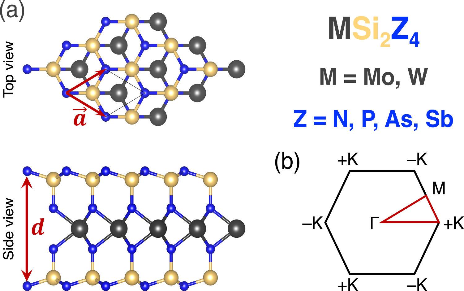
Subsequent density functional theory (DFT) calculations led to prediction of a large class of these new 2D vdW materials with general formula (with - Group-2 or transition-metal elements, - Group-13 or -14 elements, and - Group-15 or -16 elements.[7, 8] They share a common atomic structure consisting of 7 atomic layers, (see Figure 1). A 1L can be viewed as a 1L sandwiched between two layers, or alternatively, a 1L intercalated into a 1L .[7] Depending on the phases of the constituents (2 or 1 and or ), the resulting hexagonal structure has space group ( point group), identical to 2-MoS2 analogues, or space group ( point group), identical to 1-HfS2 analogues. Depending on the space group, as well as the number of valence electrons, 1L can be non-magnetic or ferromagnetic semiconductors or metals, some of which exhibit topological and superconducting behavior.[7] Numerous properties of 1L have been predicted by DFT calculations, including robust magnetic properties, [9, 10, 11] defect-induced half-metalicity,[12] high piezoelectric coefficients, [13, 14, 15, 16, 17, 18] ferroelectricity switchable via interlayer sliding, [19] high intrinsic lattice thermal conductivity, [20, 21, 22] exceptional thermoelectric performance, [23, 24, 25] anomalous spin and valley Hall effects, [7, 26, 9, 27] Ising superconductivity,[7] giant tunneling magnetoresistance,[28] tunable absorption coefficient,[29] and effective chemical adsorption properties.[30, 31, 32] Large on/off ratios were obtained in simulations of 1L transistors. [33, 34, 35, 36] This makes 1L promising candidates for device applications and stimulates further theoretical and experimental studies.
The class of 1L Si was theoretically predicted to have direct band gaps at the valleys; the only exceptions are MoSi2N4 and WSi2N4, for which the transition is between and points. Simulations suggest, however, that application of a moderate in-plane strain can shift it to the point.[37, 25, 38, 29, 39, 40] Similarly to 1L MoS2 analogues, valleys of 1L Si host two excitons A and B, originating from transitions between spin-split (valence) and (conduction) bands. The spin ordering of bands and optical selection rules are identical to 1L MoS2, where A and B transition at valleys couple to polarized light and D transition couples to linearly polarized light.[41, 5] Additionally, in compounds with Z = P, As and Sb, another two conduction bands are present above . They are involved in two higher-energy excitonic transitions A* and B* with circular polarizations opposite to A and B at given valley, and a linearly polarized D* transition.
Despite numerous studies of electronic structure of 1L Si, the literature on their quasi-particle band gaps and exciton binding energies is rather scarce. The recent GW+BSE calculations highlighted the band gap renormalization of more than 1.0 eV and exciton binding energy of several hundreds of meV.[42, 43, 44, 45, 46] The convergence of GW band gap and exciton binding energy with respect to calculation parameters was carefully checked only in Refs. [45, 46], yielding indirect and direct gap of 2.82–2.86 eV and 3.09–3.13 eV, respectively, and exciton A binding energy of 0.63 eV in 1L MoSi2N4. Furthermore, since compounds are layered materials with band edges around the points, the well-established effective modelling of exciton physics in TMDC-based systems[47, 48, 49, 50, 51, 52, 53, 54, 55, 56, 57] can be applied here as well. This would allow additional understanding of substrate and encapsulation effects on the excitonic properties, which goes beyond the GW+BSE analysis of bare 1Ls.
Due to the similarities of lattice symmetry and electronic structures of 1L 2-TMDCs and 1L , they are expected to exhibit similar optical response to external magnetic field, especially exciton -factors or diamagnetic coefficients (). The -factors, which describe the linear (Zeeman) shifts of excitonic energies, help to assign the optical peaks to specific excitonic complexes, band structure transitions, and regions of heterostructures. [58, 59, 60, 61] From the diamagnetic coefficients, which describe the quadratic energy shift, one can derive exciton reduced masses and radii.[62, 54, 63] From the technological point of view, magnetoexcitonic properties are important for valleytronic devices. For instance, numerical studies of TMDCs quantum dots have shown that large -factors are desirable to efficiently tune the spin-valley qubits at moderate external magnetic fields.[64, 65, 66] While exciton -factors are widely investigated for TMDCs,[67] such magnetooptical properties of 1L have not been reported so far.
In this work, we present a comprehensive study of electronic and excitonic properties of 1L Si (shown in Figure 1a) from DFT and model BSE (Bethe-Salpeter Equation) calculations. Chemical trends of band gaps and SOC splittings of bands at point were also analyzed. We report the binding energies and radii of excitons involving , and states at valleys. We also provide the values of their Landé -factors and diamagnetic coefficients, which describe the evolution of excitonic energies under magnetic fields. We predict large positive -factors for excitons that involve higher conduction bands emerging in = P, As and Sb compounds. Additionally, we observe a SOC-induced band inversion for the heaviest here studied material, WSi2Sb4, suggesting that this compound might host topological properties.
II Results and Discussion
II.1 Geometrical structure
The optimized lattice constants () and slab thicknesses () are shown in Table 1 together with electronic properties, which will be discussed later. Both parameters and their ratio, , monotonically increase with the mass of element. Similarly to 2-TMDCs, Mo and W compounds with the same have almost identical lattice constants (their relative difference does not exceed 0.2%), which enables to create nearly commensurate MoSi/WSi heterobilayers with interlayer twist angles of 0∘ and 60∘.
| System | [Å] | [Å] | [eV] | [meV] | [meV] | [meV] |
|---|---|---|---|---|---|---|
| MoSi2N4 | 2.900 | 7.003 | 2.021(1.787)/2.487(2.350) | 129/169 | 3/17 | - |
| MoSi2P4 | 3.453 | 9.347 | 0.621/0.864 | 137/202 | 4/30 | 87/112 |
| MoSi2As4 | 3.600 | 9.905 | 0.512/0.684 | 179/289 | 16/58 | 113/160 |
| MoSi2Sb4 | 3.879 | 10.882 | 0.262/0.364 | 262/422 | 25/91 | 146/232 |
| WSi2N4 | 2.905 | 7.014 | 2.162(2.107)/2.660(2.672) | 403/502 | 10/40 | - |
| WSi2P4 | 3.457 | 9.350 | 0.297/0.433 | 439/609 | 7/78 | 219/269 |
| WSi2As4 | 3.603 | 9.902 | 0.211/0.258 | 503/740 | 25/121 | 266/341 |
| WSi2Sb4 | 3.885 | 10.879 | 0.032/0.186 | 560/953 | 32/186 | 306/423 |
The stability of the considered compounds is confirmed by their phonon band structures, which show no imaginary phonon modes, see Figure S1. The phonon dispersion relation and element-projected density of states show distinct three regions: i) high-frequency dominated by N and Si atoms, ii) medium-frequency involving all elements, and iii) the low-frequency dominated by transition-metal and As or Sb. For the heavier layers, region i) has only contributions from silicon, whereas regions ii) and iii) merge together. Overall, the three regions are separated by smaller or larger energy gaps.
II.2 Electronic structure
Electronic band structures of 1L Si calculated using PBE without and with SOC are shown in Figure 2. The valence band maximum (VBM) of MoSi2N4 and WSi2N4 is located at point, 233 meV and 54 meV above the band extrema at , respectively. For the other compounds, VBM shifts to the point, which is more than 200 meV higher than valence band at . The conduction band minimum (CBM) is always located at the point, with secondary band extremum at or near point. The energetic separation between conduction band valleys at and points is the smallest for WSi2N4 (156 meV) and exceeds 200 meV for all other compounds. As a consequence, MoSi2N4 and WSi2N4 have indirect fundamental band gaps between and points, and all other compounds are direct gap semiconductors with transitions at . The direct gap materials have also another higher energy minimum in conduction band (CBM+1; ) at , which approaches the CBM with increasing the mass of . These additional minima result in higher-energy excitonic transitions (see Figure 2 and Section II.3).
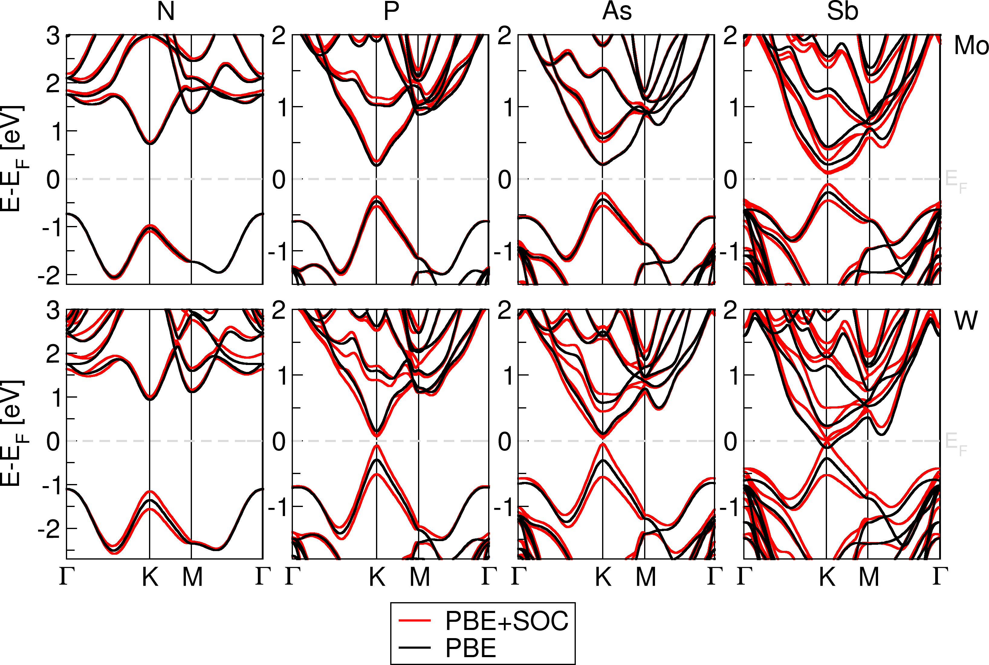
The band structures and resulting bang gap values were also recalculated with a higher-level density functional, namely HSE06, and the results are shown in Figure S2 , along with PBE band structures. In all cases, HSE06 yields larger band gaps than PBE, as shown in Table 1 and Figure S3. The main difference between both methods is that the VBM of WSi2N4 shifts to , making it also a direct gap material. All the other chemical trends of band gaps are preserved (see Figure S3).
The calculated band gap values are given in Table 1 and show the following general trends: the values of Mo-based compounds are generally larger than these of heavier W-based compounds with the same , except for nitrogen. When increasing the mass of , the band gaps decrease, with the largest reduction from N to P (see Figure S3). MoSi2N4 and WSi2N4 exhibit the largest gaps in the visible light range, while the other compounds have their gaps in the infrared regime.
SOC in non-centrosymmetric materials, as studied here, can lift the spin degeneracy of electronic bands, leading to spin-split bands along the - and - directions (see Figure 2). We define the spin splittings of , , and bands at points ( point group) as , , and , respectively, using the double group (with SOC) irreducible representations. Their magnitudes are given in Table 1 and the resulting trends are shown in Figure S4. For both functionals, the spin ordering of bands is identical to the case of 1L MoS2, with a crossing of and bands near the point. The values are in good agreement with previous theoretical reports.[37] Depending on the employed density functional, they are in the ranges of 130 – 950 meV for , 3 – 190 meV for , and 90 – 420 meV for . As expected, the splittings are higher for W-based compound and monotonically increase with the mass of .
At the HSE06 level, in WSi (with = P, As, Sb) exceeds the largest measured value for 1L WSe2 (513 meV [68]), one of the heaviest 2-TMDC. Furthermore, all compounds have significant values, even larger than the only experimental value in the 1L WSe2 (14 meV).[69] Such large spin splittings of bands would yield significant energetic resolution of excitonic peaks even at room temperature, as it was already shown for MoSi2N4.[6].
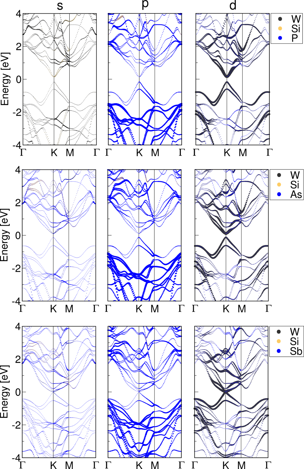
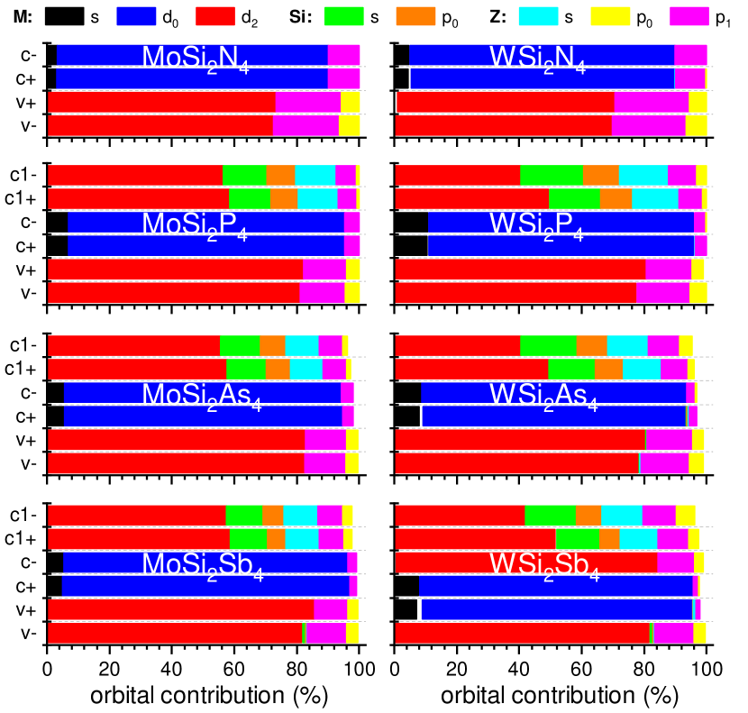
The atomic-orbital decomposition of wave function on the bands structures of MoSi2N4 and WSi2N4 are shown in Figure S5. The band edges are dominated by states that originate from transition-metal atom orbitals. This orbital character is also shared by all the other systems (see Figures S6 and S7). A detailed analysis of orbital contributions is provided in Figure S8. The states at the point are in 80% composed of ( and ) orbitals of transition-metal atoms with small admixture of () and ( and ) orbitals of pnictogenes. The states are constructed in 90% by ( orbitals of transition-metal atoms with a small contribution of metal and orbitals. The upper conduction states are still dominated by transition-metal atoms orbitals (40-60%), but with a significant contribution of other orbitals: and of Si, and and of pnictogenes.
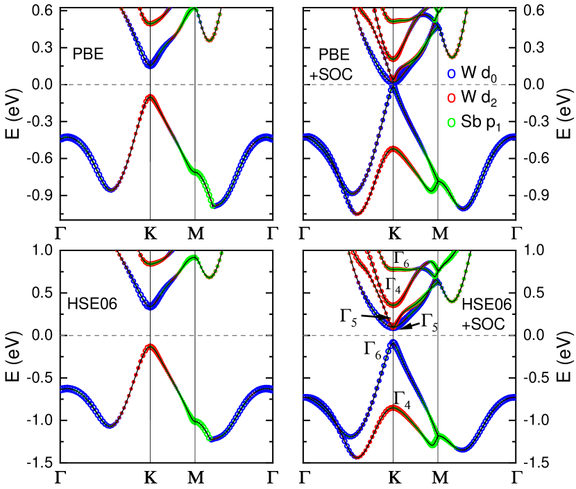
It is worth noting that the heaviest of the considered compounds, WSi2Sb4, exhibits the largest SOC effects due to the presence of two heavy elements (cf. Figure S9). Examining the orbital composition of and bands, we observe a reordering of the spin-split bands and with respect to all the other compounds. Simultaneously, analysis of the wave function symmetry reveals a change of the irreducible representations of the considered bands. Such a feature is an indication of SOC-induced transition from a trivial to a topological state[70, 71] (more detailed analysis of the wave function symmetry and topological invariants of the considered bands is beyond the scope of present work).
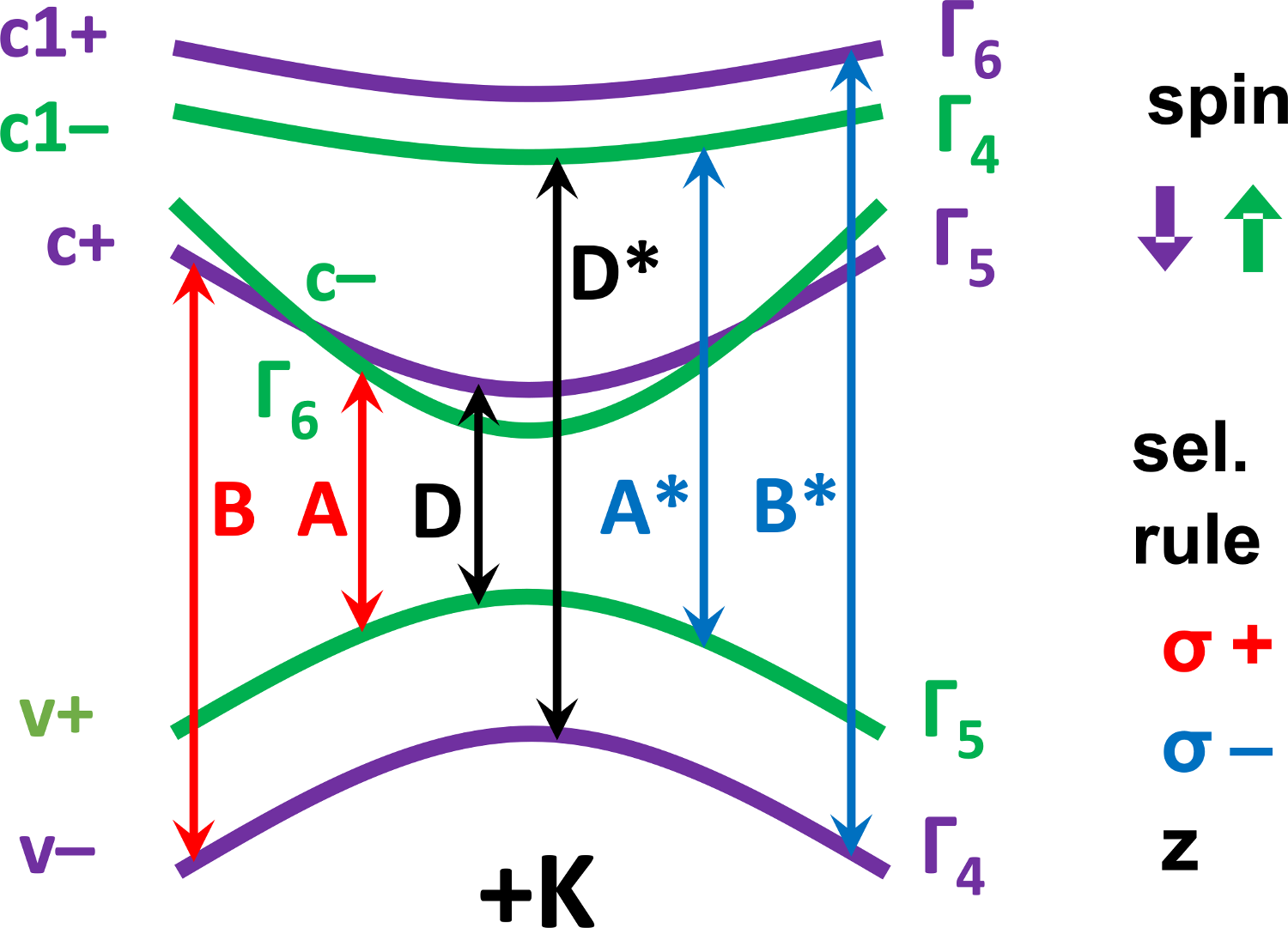
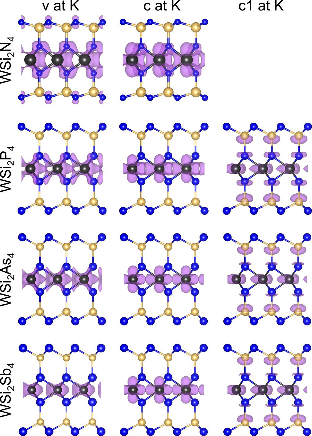
The spin ordering of spin-split bands at leads to specific valley optical selection rules, sketched in Figure 3: spin-conserving transitions A and B () couple to light at valleys. Interestingly, transitions to the upper conduction band (), which we refer to as A* and B*, have opposite selection rules – they couple to light at . This means that a photon with adequate energy and circular polarization can selectively populate or conduction states in valleys. This multiple-folded valley property makes 1L Si promising candidates for multiple-information processing.[72]. Additionally, there are two -polarized transitions D and D* ( and ). The remaining two transitions, and , are optically inactive. WSi2Sb4 exhibits distinct selection rules, as a consequence of aforementioned band inversion (see Figure S9).
The complete list of all the transition energies from PBE and HSE06 simulations, together with their optical polarizations and dipole strengths from PBE calculations, are provided in Tables S1–S8. Transitions A and B have the largest dipole strengths, compared with A* and B* which are one order of magnitude less intense, but should also be observable in optical reflection measurements and modulation spectroscopy techniques, like electro- and photoreflectance. On the other hand, the A* and B* energies are approximately twice larger than for A and B. This, along with their selection rules opposite to A and B, makes the = P, As, and Sb compounds promising candidates to study quantum interference effects, like electromagnetically induced transparency, recently reported for 1L and twisted bilayer WSe2.[73, 74, 57] Therefore, a deeper insight into the properties of A* and B* transitions in such materials is desirable. The -polarized transitions D and D* are 3–4 orders of magnitude less intense, similar to 1L 2-TMDCs.[75] The dipole strengths of A, B and D (A*, B* and D*) transitions decrease (increase) with the mass of and are generally larger for W-based compounds.
It is worth noting that the HSE06 calculated band gaps of MoSi2N4 (direct 2.35 eV and indirect 2.49 eV), as well as the energy of B transition and VBM spin splitting at of 2.67 eV and 190 meV, respectively, are in decent agreement with values of 1.94 eV, 2.21 eV, 2.35 eV, and 140 meV measured at room temperature for this compound.[6] On the other hand, the only converged GW+BSE calculations available in the literature yield 2.5 eV energy of exciton A,[45] almost identical to our HSE06 result, which does not take into account many-body effects and exciton binding energy. It indicates that HSE06 may give a good estimate and chemical trends of band gaps and spin splittings also for other compounds of 1L family, at a moderate computational cost.
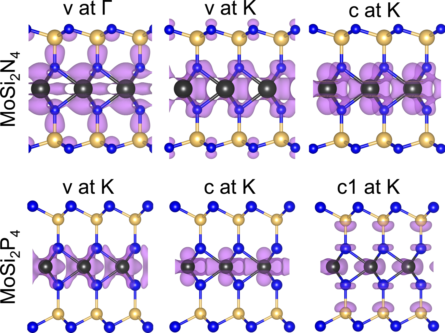
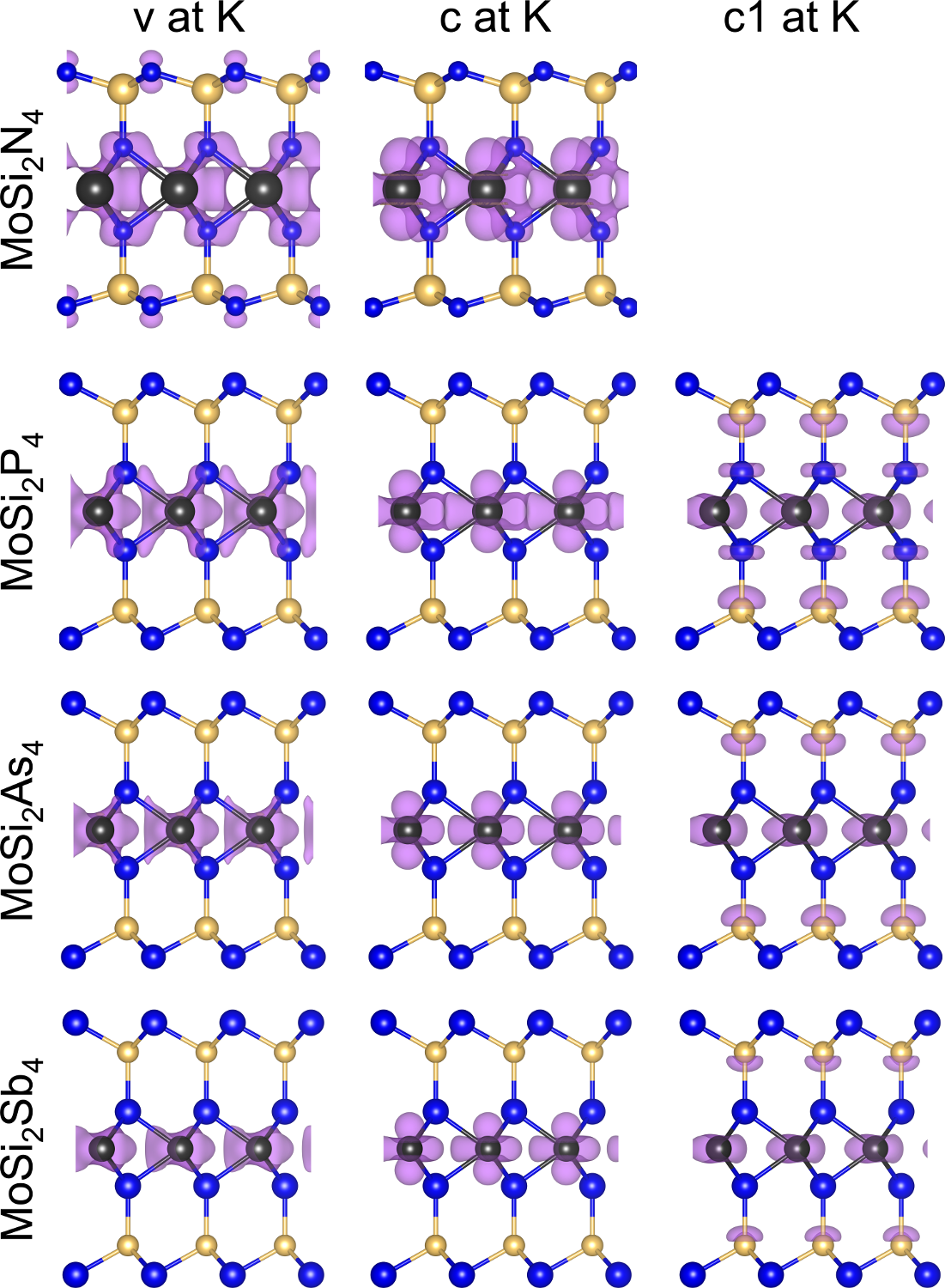
Next, we calculated and plotted the real-space wave function at the relevant -points. Figure 4 shows exemplary wave function plots for 1L MoSi2N4 and MoSi2P4 (see Figures S10 and S11 for all other compounds). In general, the electron and hole states are situated at the point, except for MoSi2N4, in which the hole states are at . The wave function plots show the localization of states at to the middle part of the layer, mostly on the transition-metal atom and, for lighter materials, on the inner atoms. Increasing the mass of , the localization increases and eventually it is dominated by just the metal atom for Sb-based compounds. Since the atom layer is situated in the middle of a 7-atomic-layer slab, the electron and hole states are effectively screened inside the monolayer. Yao et al. [76] showed also that this behaviour persists for bilayers, showing layer-independent electronic properties (e.g., band gaps). This is different for 1L MoSi2N4, where hole states are delocalized to all atomic layers. This is also true for the higher-energy electron states (). Such differences in the carrier state localization may result in different exciton lifetimes.
II.3 Excitonic properties
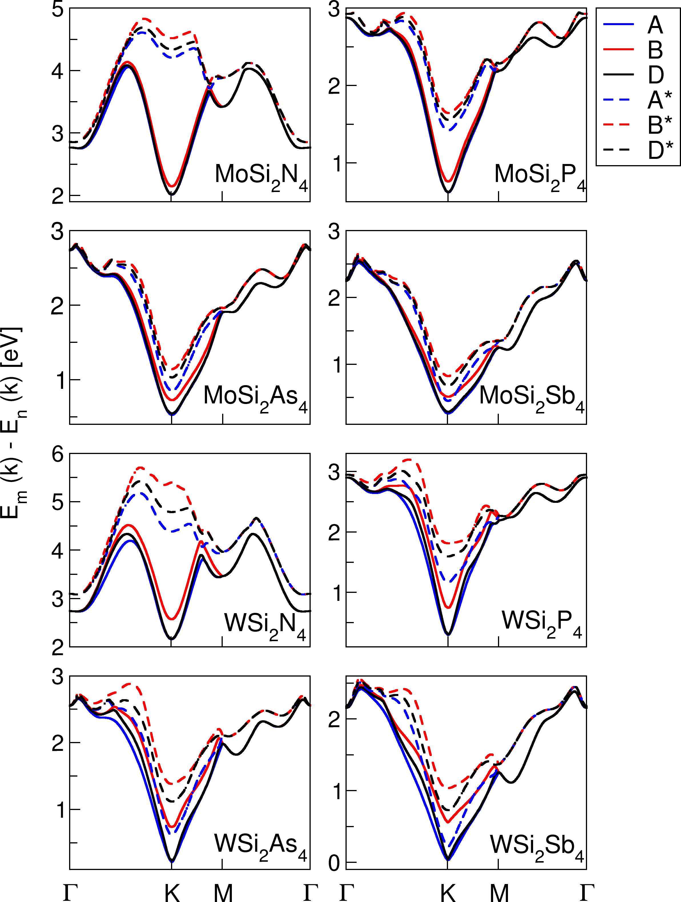
In order to host a stable excitonic state, the dispersion of its electron and hole band energy difference , (, , ) must have a local minimum in the reciprocal space. We used the calculated band structures to check that this condition is fulfilled for all the considered transitions in all compounds, see Figures S12 and S13. The band effective masses and screening lengths of 1L MoSi, provided in Table S1, as obtained from PBE calculations, are used in model BSE calculations, as described in Section IV. The reduced masses (see Tables S2–9) of most of the excitons are similar to the case of 1L TMDCs,[67] except for WSi, = P, As, Sb, where they may be lower than 0.1. The values of are increasing with the decrease of band gap and are similar to or exceed the typical values of 1L 2-TMDCs.[47] The resulting exciton binding energies, , are provided in Tables S2–S9. The of all excitons in MoSi2N4 and WSi2N4 are of the order of 450–500 meV, with the highest values for indirect excitons, as a consequence of their low reduced masses. They are comparable to the binding energies observed in 1L 2-TMDCs,[5] which should ensure the stability of excitons against thermal dissociation. The values for A*, B* and D* excitons are similar or slightly larger than for A, B, and D, and show a systematic decrease, along with the decreasing band gap for heavier atoms.
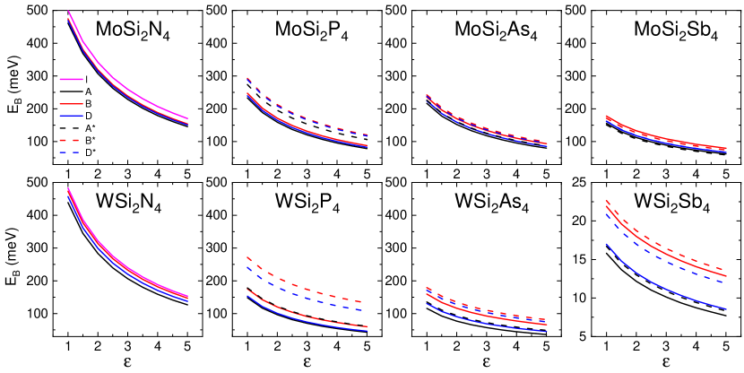
The binding energy of an exciton is strongly sensitive to its dielectric environment. Model BSE enables to study this dependence by introducing an effective relative dielectric constant () of the systems’ surroundings (see Section IV). As shown in Figure S14 , decreases with increasing , as in case of 1L 2-TMDCs. Figure 5 presents this dependence for A exciton in all the considered compounds in three typical situations: in vacuum (), on SiO substrate ( [79], ; see Section IV for details) and encapsulated in hBN ( [80]), compared to the corresponding values of 1L WSe2 and Group-6 bulk TMDCs.[81] As expected, is significantly smaller for SiO2 substrate or hBN-encapsulation, compared with the vacuum value.
For N-based compounds, the binding energies are comparable to the case of 1L WSe2, which exhibits the largest of 1L 2-TMDCs. The values gradually decrease with heavier atoms, for WSi2P4 and WSi2As4 reaching the range of Group-6 bulk TMDCs. The binding energy of WSi2Sb4 is below the thermal energy at room temperature. It should be noted that our of A exciton from model BSE for MoSi2N4 (0.46 eV) is in a decent agreement with GW+BSE calculations of Wang et al. [45] (0.63 eV). This discrepancy can be attributed to the different values of effective masses and the screening length obtained within different approaches.
II.4 Exciton -factors and diamagnetic coefficients
After analyzing the electronic structure and exciton binding energies, we focused on the magnetooptical properties of 1L Si. First, the convergence of orbital angular momenta of bands and exciton -factors with respect to the number of states involved in the summation in Equation (2) must be performed (see Figures 6(a) and (b) for exemplary MoSi2As4 results). The largest contribution to is at the band gap (dashed vertical line). Around 800 bands are required to converge the -factors to the precision of 0.1. This is more than in the case of 1L TMDCs, where around 300–500 bands are required.[60, 82, 75] The converged values of orbital angular momenta for all compounds are given in Table S10. We observe that for and are positive and of the same order as for TMDCs. Interestingly, of and in WSi2P4 and WSi2As4 are much larger than in the other compounds. This is due to a large contribution of in the summation of Equation (2). The values for = P, As, Sb are negative. For VBM at , the orbital angular momentum is smaller than 0.01 in MoSi2N4 and smaller than 0.03 in WSi2N4. The -factors of A and B excitons are negative and significantly smaller in magnitude than these for 1L TMDCs, where values of around -4 are observed.[60, 83, 75] This indicates that simplistic models, which are based on orbital compositions of band edges and their effective masses, cannot accurately predict in Si. The -factor of D exciton is lower from by more than -4, which is due to the spin-flip contribution. The -factors of A*, B* and D* excitons are positive and have much larger magnitude than for A, B and D. The former origins from the inverted selection rules ( light couples to valleys). The latter is caused by positive . As a consequence, the Zeeman splittings for A* and B* excitons are approximately 4–5 times larger than for A and B in Si and 1L TMDCs. To the best of our knowledge, these are the largest values reported for hexagonal monolayers so far. This allows to achieve a sizeable spin and valley splitting of A* and B* based states in MoSi quantum dots at lower magnetic fields than in the case of TMDCs.[64]
As the standard DFT calculations with PBE functional severely underestimate the electronic band gaps, the resulting are usually overestimated, due to the energy denominator in Equation (2). This can be corrected on the easiest possible level by applying the scissor shift to the conduction bands: for . Figures 6(c) and (d) present the influence of on the orbital angular momenta and exciton -factors. When increasing the band gap of MoSi2As4 to HSE06 value, for , significantly decrease with scissor, while the values for and slightly increase. As a consequence, the magnitudes of excitonic -factors decrease. The largest slope is observed for A*, B* and D* excitons, while the values for A and B are nearly constant. The trends for A, B and D excitons are similar to the case of 1L TMDCs.[60, 75]
The -factors of all the considered excitons are shown in Figure 7. Overall, are larger for W- than for Mo-based materials. As already discussed, for a given compound, the -factors of A and B excitons are similar and do not depend on scissor correction. Increasing the mass of element, their magnitudes decrease (increase) for materials containing Mo (W). The splitting increases with the mass of and becomes sizeable in MoSi2Sb4. For all compounds, except WSi, = P, As, Sb, the -factors of exciton D are in the range of -7 – -9. The -factors of A*, B*, and D* are always positive and reduce with increase in mass of element. Their splitting is significantly larger than for A and B. As in the case of MoSi2As4, the influence of scissor correction is more prominent for I, D, A*, B*, and D* than for A and B excitons. The effect is noticeably large for D and A* in WSi2P4 and WSi2As4, which stems from a strong reduction of for and by scissor correction (see Tables S7 and S8).

In addition to zero-momentum excitons, based on direct transitions at valleys, in MoSi2N4 and WSi2N4, we consider also finite-momentum excitons , connected to indirect fundamental band gaps (VBM at and CBM at ) of these compounds. Their values are dominated by , as . Consequently, and decreases with the scissor correction.
The -factors in WSi2Sb4 do not follow the common trend. In contrast to the other materials, and ( and ) are positive (negative), which stems from the modified selection rules and strongly different for , and , which are additionally almost insensitive to the scissor correction (see Table S10). This is related to the SOC-induced band inversion in valleys and requires further investigations, which are beyond the scope of this work.
Finally, the quadratic part of exciton energy shift in magnetic field is quantified by the diamagnetic coefficient. In case of 1L TMDCs, where values are lower than 1 eV T-2, very high magnetic fields are required (20 T) to observe the diamagnetic shifts.[54] We predict the values of diamagnetic coefficients in MoSi basing on exciton reduced masses from DFT and expectation values of exciton radii from BSE calculations, respectively. The values of and are provided in Tables S2–S9. The exciton radii generally increase with the mass of element. Consequently, diamagnetic coefficients also increase, reaching few or few tens of eV T-2 for excitons with low reduced mass and large in WSi, = P, As, and Sb. Such large values of might allow to observe significant diamagnetic shifts even at low magnetic fields.
III Conclusion
We have investigated electronic properties of selected 1L Si employing first-principles calculations. Considered materials are direct gap semiconductors with transition at the point (except for Si2N4, for which the fundamental transition is between and ). They also show emerging upper conduction bands , resulting in higher-energy excitonic transitions. The electron and hole wave functions are mostly confined to the transition-metal atoms plane and the localization increases with the mass of elements. The band gaps at point span a range of 2.66–0.19 eV and the spin splittings of valence, conduction, and upper conduction bands range from about 20 meV up to nearly 1 eV. We have shown that the upper conduction states give rise to higher energy direct transitions with finite dipole strengths and circular optical selection rules.
We have studied the excitonic properties of 1L Si from the effective Bethe-Salpeter equation. Exciton binding energies and radii in range of 0.016–0.50 eV and 12–120 Å, respectively, are predicted. We provide the dependence of binding energies on the dielectric constant, highlighting the typical experimental conditions. We have investigated the magnetooptical properties of considered excitons, quantified by their Lande -factors and diamagnetic coefficients. The -factors of band edge excitons are similar to the case of 1L 2-TMDCs, while the values for higher energy transitions are positive and range from 6 to 30. Such large values have never been observed in hexagonal 1Ls before. The calculated diamagnetic coefficients also reach high values, up to 84 meV T-2. Combining both, significant excitonic energy shifts and splittings are expected under relatively low magnetic fields. Finally, we observed a SOC-induced band inversion in WSi2Sb4, which might indicate its topological nature and leads to peculiar values of its magnetooptical coefficients.
Thanks to their electronic and excitonic properties, 1L Si compounds are important new members in 2D materials family, as they offer a number of robust excitons with significant magnetooptical responses. This makes the studied compounds and their layered heterostructures an attractive platform for studying fundamental spin-valley physics and potential use in optoelectronic, spintronic, and valleytronic devices. In these terms, 1L Si can be considered as complementary to 1L 2-TMDCs, and desire further experimental and theoretical studies.
IV Experimental Section
Computational Details
All DFT calculations were carried out using the Vienna ab-initio simulation package (VASP).[84] The projector augmented wave (PAW) technique was used to describe the ionic potentials. For the geometry optimization, we employed the generalized gradient approximation (GGA) of the exchange correlation-functional within Perdew-Burke-Ernzerhof (PBE) parametrization[85] together with the D3 dispersion correction for vdW interaction of Grimme.[86] The plane-wave cutoff energy and the total energy convergence criterion were set to 500 eV and 10-8 eV, respectively. The geometrical structures were fully optimized until the interatomic forces and stress tensor components were lower than eV Å-1 and 0.1 kbar, respectively. A vacuum region of at least 15 Å was used to avoid spurious interactions between the periodically repeated layers. The BZ integrations were performed on a -centered 12121 Monkhorst-Pack -grid with a Gaussian smearing of 0.1 eV. PBE and Heyd-Scuseria-Ernzerhof (HSE06) hybrid functional[87] were adopted to calculate the electronic band structures. SOC was taken into account during geometrical optimization and electronic structure calculations. The irreducible representations of electronic bands at points were determined from the analysis of wave function symmetries. The density functional perturbation theory approach was used to calculate phonon dispersion spectra as implemented in PHONOPY code[88] with a 441 supercell. The partial charge densities (PCD) were calculated using PBE functional. Structural illustrations and the band decomposed PCD plots in real space were created using the 3D visualization package VESTA.[89]
To compute the exciton binding energies and wave functions, we used the effective Bethe-Salpeter equation (BSE)[90, 91, 52] with the electron-hole interaction mediated by Rytova-Keldysh (RK) potential.[92, 93] The input parameters required for the effective BSE are: (i) the effective masses of the relevant conduction and energy bands and (ii) the parameters for the RK potential, namely, the screening length of the 2D material, , and the effective relative dielectric constant of the surrounding media, , with being the dielectric constant of the top (bottom) material. Particularly, the effective masses of electrons and holes were obtained from quadratic fits to the band edges near and points, while the screening length was calculated using the in-plane components of static dielectric tensors including the ionic contributions (following Ref. [47]). These parameters are given in Table S1. of the Supplementary Material (SM) for all studied compounds. Finally, the effective BSE is solved numerically on a 2D -grid sampled with 121121 -points in a square region with sides ranging from to 0.5 , yielding a -point spacing of along each direction. Furthermore, to improve the convergence, the RK potential was averaged in a 2D -grid submesh of 121121 points covering an area of .
The dependence of exciton energy on the applied external out-of-plane magnetic field is described as , where is the exciton -factor, is the Bohr magneton, is the magnetic field induction, and is the diamagnetic coefficient. The linear term is referred to as Zeeman shift and the quadratic term as diamagnetic shift. Experimentally, is conveniently determined from a linear fit to and from a quadratic fit to .
The exciton -factors were calculated within the bands summation method described in Ref. [60]. The linear shift of band energy at point under external out-of-plane magnetic field is quantified by a -factor of a Bloch state expressed as:
| (1) |
where and are the -components of orbital and spin angular momenta, respectively. The orbital angular momentum is evaluated from a summation formula:[94, 95]
| (2) |
where is the rest mass of the electron, is the Bloch state energy, are the momentum operator matrix elements between and states in directions, and the summation runs over all states in the basis set. For the relevant low-energy bands, we considered . The Zeeman splitting of exciton = A, B, D, A*, B* and D* is then described by excitonic -factor:
| (3) |
where , , , and the sign depends on optical selection rules at point. Determination of sign of the indirect exciton -factor requires analysis of the phonon-mediated optical selection rules[96], which is beyond the scope of our work. Therefore, we provide the absolute value .
Diamagnetic coefficients of direct excitons were evaluated as , where is the elementary charge, is the exciton reduced mass calculated from electron and hole effective masses and , respectively, and is the expectation value of the squared exciton radius in real space. The exciton radii were extracted from the exciton wave functions calculated with the effective BSE.
Acknowledgements
We thank Kai-Qiang Lin, Maciej Molas, Maciej Bieniek, Jarosław Pawłowski, Thomas Brumme and Florian Arnold for stimulating discussions. TW, UA, MSR, AK thank the Deutsche Forschungsgemeinschaft (project GRK 2247/1 (QM3) and project CRC1415, number 417590517) for financial support and the high-performance computing center of ZIH Dresden for computational resources. TW acknowledges the financial support of National Science Centre, Poland within Project No. 2021/41/N/ST3/04516. AK acknowledges association with priority program (project SPP2244 (2DMP)). PEFJ acknowledges the financial support of the Deutsche Forschungsgemeinschaft (DFG, German Research Foundation) SFB 1277 (Project-ID 314695032, projects B07 and B11) and SPP 2244 (Project No. 443416183). M.S.R acknowledges financial support by project SMART, financed by the Volkswagen Foundation as part of the program “Niedersachsisches Vorab - Digitalisierung in den Natururwissenschaften.
References
- [1] K. Khan, A. K. Tareen, M. Aslam, R. Wang, Y. Zhang, A. Mahmood, Z. Ouyang, H. Zhang, Z. Guo, Recent developments in emerging two-dimensional materials and their applications, volume 8, Royal Society of Chemistry, 2020.
- [2] K. S. Novoselov, A. K. Geim, S. V. Morozov, D. Jiang, Y. Zhang, S. V. Dubonos, I. V. Grigorieva, A. A. Firsov, Science 2004, 306, 5696 666.
- [3] K. F. Mak, C. Lee, J. Hone, J. Shan, T. F. Heinz, Physical Review Letters 2010, 105, 13 136805.
- [4] T. Mueller, E. Malic, npj 2D Materials and Applications 2018, 2, 1 1.
- [5] G. Wang, A. Chernikov, M. M. Glazov, T. F. Heinz, X. Marie, T. Amand, B. Urbaszek, Reviews of Modern Physics 2018, 90, 2 21001.
- [6] Y. L. Hong, Z. Liu, L. Wang, T. Zhou, W. Ma, C. Xu, S. Feng, L. Chen, M. L. Chen, D. M. Sun, X. Q. Chen, H. M. Cheng, W. Ren, Science 2020, 369, 6504 670.
- [7] L. Wang, Y. Shi, M. Liu, A. Zhang, Y.-L. Hong, R. Li, Q. Gao, M. Chen, W. Ren, H.-M. Cheng, Y. Li, X.-Q. Chen, Nature Communications 2021, 12, 1 2361.
- [8] K. S. Novoselov, National Science Review 2020, 7, 12 1842.
- [9] Q. Cui, Y. Zhu, J. Liang, P. Cui, H. Yang, Physical Review B 2021, 103, 8 085421.
- [10] J. Chen, Q. Tang, Chemistry - A European Journal 2021, 27, 38 9925.
- [11] Y. Li, J. Wang, G. Yang, Y. Liu, Annalen der Physik 2021, 533, 12 2100273.
- [12] A. Ray, S. Tyagi, N. Singh, U. Schwingenschlögl, ACS Omega 2021, 6, 45 30371, pMID: 34805668.
- [13] S. D. Guo, Y. T. Zhu, W. Q. Mu, W. C. Ren, Epl 2020, 132, 5.
- [14] S.-D. Guo, W.-Q. Mu, Y.-T. Zhu, R.-Y. Han, W.-C. Ren, Journal of Materials Chemistry C 2021, 9, 7 2464.
- [15] S. D. Guo, Y. T. Zhu, W. Q. Mu, L. Wang, X. Q. Chen, Computational Materials Science 2021, 188, December 2020 110223.
- [16] B. Mortazavi, B. Javvaji, F. Shojaei, T. Rabczuk, A. V. Shapeev, X. Zhuang, Nano Energy 2021, 82 105716.
- [17] S.-D. Guo, W.-Q. Mu, Y.-T. Zhu, X.-Q. Chen, Physical Chemistry Chemical Physics 2020, 22, 48 28359.
- [18] X. Guo, S. Guo, Journal of Semiconductors 2021, 42, 12 122002.
- [19] T. Zhong, Y. Ren, Z. Zhang, J. Gao, M. Wu, Journal of Materials Chemistry A 2021, 9, 35 19659.
- [20] J. Yu, J. Zhou, X. Wan, Q. Li, New Journal of Physics 2021, 23, 3 033005.
- [21] C. Shen, L. Wang, D. Wei, Y. Zhang, G. Qin, X.-Q. Chen, H. Zhang, Physical Chemistry Chemical Physics 2022, 24, 5 3086.
- [22] Y. Yin, M. Yi, W. Guo, ACS Applied Materials & Interfaces 2021, 13, 38 45907.
- [23] Y. Huang, X. Zhong, H. Yuan, H. Chen, Europhysics Letters 2022, 2, 1 0.
- [24] A. Bafekry, M. Faraji, D. M. Hoat, M. Shahrokhi, M. M. Fadlallah, F. Shojaei, S. A. H. Feghhi, M. Ghergherehchi, D. Gogova, Journal of Physics D: Applied Physics 2021, 54, 15 155303.
- [25] X.-S. Guo, S.-D. Guo, Chinese Physics B 2021, 30, 6 067102.
- [26] S. Li, Q. Wang, C. Zhang, P. Guo, S. A. Yang, Physical Review B 2021, 104, 8 085149.
- [27] W. Zhou, L. Wu, A. Li, B. Zhang, F. Ouyang, The Journal of Physical Chemistry Letters 2021, 12, 48 11622.
- [28] Q. Wu, L. K. Ang, Applied Physics Letters 2022, 120, 2 022401.
- [29] C.-c. Jian, X. Ma, J. Zhang, X. Yong, The Journal of Physical Chemistry C 2021, 125, 28 15185.
- [30] A. Bafekry, M. Faraji, M. Fadlallah, A. Abdolahzadeh Ziabari, A. Bagheri Khatibani, S. Feghhi, M. Ghergherehchi, D. Gogova, Applied Surface Science 2021, 564, April 150326.
- [31] Z. Cui, Y. Luo, J. Yu, Y. Xu, Physica E: Low-dimensional Systems and Nanostructures 2021, 134, April 114873.
- [32] Y. He, Y.-h. Zhu, M. Zhang, J. Du, W.-h. Guo, S.-m. Liu, C. Tian, H.-x. Zhong, X. Wang, J.-j. Shi, Physical Chemistry Chemical Physics 2022, 24, 4 2110.
- [33] X. Sun, Z. Song, N. Huo, S. Liu, C. Yang, J. Yang, W. Wang, J. Lu, Journal of Materials Chemistry C 2021, 9, 41 14683.
- [34] H. Zhao, G. Yang, Y. Liu, X. Yang, Y. Gu, C. Wei, Z. Xie, Q. Zhang, B. Bian, X. Zhang, X. Huo, N. Lu, ACS Applied Electronic Materials 2021, 3, 11 5086.
- [35] K. Nandan, B. Ghosh, A. Agarwal, S. Bhowmick, Y. S. Chauhan, IEEE Transactions on Electron Devices 2022, 69, 1 406.
- [36] N. Ghobadi, M. Hosseini, S. B. Touski, IEEE Transactions on Electron Devices 2022, 69, 2 863.
- [37] S. Li, W. Wu, X. Feng, S. Guan, W. Feng, Y. Yao, S. A. Yang, Physical Review B 2020, 102, 23 235435.
- [38] H. Ai, D. Liu, J. Geng, S. Wang, K. H. Lo, H. Pan, Physical Chemistry Chemical Physics 2021, 23, 4 3144.
- [39] S. Babaee Touski, N. Ghobadi, Journal of Physics D: Applied Physics 2021, 54, 48 485302.
- [40] Z. Wang, X. Kuang, G. Yu, P. Zhao, H. Zhong, S. Yuan, Physical Review B 2021, 104, 15 155110.
- [41] H. Zeng, J. Dai, W. Yao, D. Xiao, X. Cui, Nature Nanotechnology 2012, 7, 8 490.
- [42] S. Sheoran, D. Gill, A. Phutela, S. Bhattacharya 2022.
- [43] M. Tian, C. Wei, J. Zhang, J. Wang, R. Yang, Physical Review B 2021, 103, 19 195305.
- [44] P. Yadav, B. Khamari, B. Singh, K. V. Adarsh, A. Agarwal 2022, 4 1.
- [45] Y. Wu, Z. Tang, W. Xia, W. Gao, F. Jia, Y. Zhang, W. Zhu, W. Zhang, P. Zhang, npj Computational Materials 2022, 8, 1 129.
- [46] H. Zhong, G. Zhang, C. Lu, S. Gao 2022, 4 1.
- [47] T. C. Berkelbach, M. S. Hybertsen, D. R. Reichman, Physical Review B 2013, 88, 4 045318.
- [48] A. Chernikov, T. C. Berkelbach, H. M. Hill, A. Rigosi, Y. Li, O. B. Aslan, D. R. Reichman, M. S. Hybertsen, T. F. Heinz, Phys. Rev. Lett. 2014, 113 076802.
- [49] B. Scharf, G. Xu, A. Matos-Abiague, I. Žutić, Phys. Rev. Lett. 2017, 119 127403.
- [50] A. V. Stier, N. P. Wilson, K. A. Velizhanin, J. Kono, X. Xu, S. A. Crooker, Phys. Rev. Lett. 2018, 120 057405.
- [51] Y. Cho, T. C. Berkelbach, Phys. Rev. B 2018, 97 041409(R).
- [52] K. Zollner, P. E. Faria Junior, J. Fabian, Phys. Rev. B 2019, 100 195126.
- [53] K. Zollner, P. E. Faria Junior, J. Fabian, Phys. Rev. B 2019, 100 085128.
- [54] M. Goryca, J. Li, A. V. Stier, T. Taniguchi, K. Watanabe, E. Courtade, S. Shree, C. Robert, B. Urbaszek, X. Marie, S. A. Crooker, Nature Communications 2019, 10, 1 4172.
- [55] K. Zollner, P. E. Faria Junior, J. Fabian, Phys. Rev. B 2020, 101 085112.
- [56] J. C. G. Henriques, G. Catarina, A. T. Costa, J. Fernández-Rossier, N. M. R. Peres, Phys. Rev. B 2020, 101 045408.
- [57] K.-q. Lin, C. S. Ong, S. Bange, P. E. Faria Junior, B. Peng, J. D. Ziegler, J. Zipfel, C. Bäuml, N. Paradiso, K. Watanabe, T. Taniguchi, C. Strunk, B. Monserrat, J. Fabian, A. Chernikov, D. Y. Qiu, S. G. Louie, J. M. Lupton, Nature Communications 2021, 12, 1 5500.
- [58] A. Ciarrocchi, D. Unuchek, A. Avsar, K. Watanabe, T. Taniguchi, A. Kis, Nature Photonics 2019, 13, 2 131.
- [59] K. L. Seyler, P. Rivera, H. Yu, N. P. Wilson, E. L. Ray, D. G. Mandrus, J. Yan, W. Yao, X. Xu, Nature 2019, 567, 7746 66.
- [60] T. Woźniak, P. E. Faria Junior, G. Seifert, A. Chaves, J. Kunstmann, Physical Review B 2020, 101, 23 235408.
- [61] M. Zinkiewicz, T. Woźniak, T. Kazimierczuk, P. Kapuscinski, K. Oreszczuk, M. Grzeszczyk, M. Bartoš, K. Nogajewski, K. Watanabe, T. Taniguchi, C. Faugeras, P. Kossacki, M. Potemski, A. Babiński, M. R. Molas, Nano Letters 2021, 21, 6 2519.
- [62] D. C. Rogers, J. Singleton, R. J. Nicholas, C. T. Foxon, K. Woodbridge, Phys. Rev. B 1986, 34 4002.
- [63] S.-Y. Chen, Z. Lu, T. Goldstein, J. Tong, A. Chaves, J. Kunstmann, L. S. R. Cavalcante, T. Woźniak, G. Seifert, D. R. Reichman, T. Taniguchi, K. Watanabe, D. Smirnov, J. Yan, Nano Letters 2019, 19, 4 2464.
- [64] A. Kormányos, V. Zólyomi, N. D. Drummond, G. Burkard, Physical Review X 2014, 4, 1 011034.
- [65] K. E. J. Goh, F. Bussolotti, C. S. Lau, D. Kotekar-Patil, Z. E. Ooi, J. Y. Chee, Advanced Quantum Technologies 2020, 3, 6 1900123.
- [66] J. Pawłowski, M. Bieniek, T. Woźniak, Physical Review Applied 2021, 15, 5 054025.
- [67] A. Arora, Journal of Applied Physics 2021, 129, 12 120902.
- [68] D. Le, A. Barinov, E. Preciado, M. Isarraraz, I. Tanabe, T. Komesu, C. Troha, L. Bartels, T. S. Rahman, P. A. Dowben, Journal of Physics: Condensed Matter 2015, 27, 18 182201.
- [69] P. Kapuściński, A. Delhomme, D. Vaclavkova, A. O. Slobodeniuk, M. Grzeszczyk, M. Bartos, K. Watanabe, T. Taniguchi, C. Faugeras, M. Potemski, Communications Physics 2021, 4, 1.
- [70] M. Kurpas, P. E. Faria Junior, M. Gmitra, J. Fabian, Physical Review B 2019, 100, 12 125422.
- [71] J. Cano, B. Bradlyn, Annual Review of Condensed Matter Physics 2021, 12, 1 225.
- [72] C. Yang, Z. Song, X. Sun, J. Lu, Physical Review B 2021, 103, 3 035308.
- [73] K.-Q. Lin, S. Bange, J. M. Lupton, Nature Physics 2019, 15, 3 242.
- [74] K.-Q. Lin, P. E. Faria Junior, J. M. Bauer, B. Peng, B. Monserrat, M. Gmitra, J. Fabian, S. Bange, J. M. Lupton, Nature Communications 2021, 12, 1 1553.
- [75] P. E. Faria Junior, K. Zollner, T. Woźniak, M. Kurpas, M. Gmitra, J. Fabian, New Journal of Physics 2022, 24, 8 083004.
- [76] H. Yao, C. Zhang, Q. Wang, J. Li, Y. Yu, F. Xu, B. Wang, Y. Wei, Nanomaterials 2021, 11, 3 1.
- [77] K. D. Pham, C. Q. Nguyen, C. V. Nguyen, P. V. Cuong, N. V. Hieu, New Journal of Chemistry 2021, 45, 12 5509.
- [78] P. Zhao, Z.-Y. Jiang, J.-M. Zheng, Y.-M. Lin, A. Du, The Journal of Physical Chemistry C 2022, 126, 27 11380.
- [79] S. M. Sze, K. N. Kwok, editors, Physics of Semiconductor Devices, chapter Appendix H: Properties of SiO2 and Si3N4, John Wiley and Sons, Ltd, 2006.
- [80] R. Geick, C. H. Perry, G. Rupprecht, Phys. Rev. 1966, 146 543.
- [81] M. Birowska, P. E. Faria Junior, J. Fabian, J. Kunstmann, Physical Review B 2021, 103, 12 L121108.
- [82] J. Förste, N. V. Tepliakov, S. Y. Kruchinin, J. Lindlau, V. Funk, M. Förg, K. Watanabe, T. Taniguchi, A. S. Baimuratov, A. Högele, Nature Communications 2020, 11, 1 4539.
- [83] T. Deilmann, P. Krüger, M. Rohlfing, Phys. Rev. Lett. 2020, 124 226402.
- [84] G. Kresse, J. Furthmüller, Physical Review B 1996, 54, 16 11169.
- [85] J. P. Perdew, K. Burke, M. Ernzerhof, Physical Review Letters 1996, 77, 18 3865.
- [86] S. Grimme, J. Antony, S. Ehrlich, H. Krieg, Journal of Chemical Physics 2010, 132, 15 154104.
- [87] M. E. J. Heyd, G. E. Scuseria, Journal of Chemical Physics 2006, 124 219906.
- [88] I. T. A. Togo, Scripta Materialia 2015, 108 1.
- [89] F. I. K. Momma, Journal of Appl. Crystallography 2011, 44 1272.
- [90] M. Rohlfing, S. G. Louie, Phys. Rev. B 2000, 62 4927.
- [91] P. E. Faria Junior, M. Kurpas, M. Gmitra, J. Fabian, Phys. Rev. B 2019, 100 115203.
- [92] N. S. Rytova, Mosc. Univ. Phys. Bull. 1967, 3, 3 18.
- [93] L. Keldysh, Sov. J. Exp. Theo. Phys. Lett. 1979, 29 658.
- [94] L. M. Roth, B. Lax, S. Zwerdling, Phys. Rev. 1959, 114 90.
- [95] M.-C. Chang, Q. Niu, Phys. Rev. B 1996, 53 7010.
- [96] E. Blundo, P. E. Faria Junior, A. Surrente, G. Pettinari, M. A. Prosnikov, K. Olkowska-Pucko, K. Zollner, T. Woźniak, A. Chaves, T. Kazimierczuk, M. Felici, A. Babiński, M. R. Molas, P. C. M. Christianen, J. Fabian, A. Polimeni, Phys. Rev. Lett. 2022, 129 067402.
V Supplementary Material
V.1 Supplementary Figures
V.2 Supplementary Tables
| MoSi2N4 | -1.66 | -0.61 | -0.55 | 0.40 | 0.45 | 51.6 | ||
|---|---|---|---|---|---|---|---|---|
| MoSi2P4 | -0.39 | -0.30 | 0.28 | 0.35 | 8.55 | -32.16 | 109.2 | |
| MoSi2As4 | -0.50 | -0.34 | 0.42 | 0.62 | 0.69 | 0.86 | 130.5 | |
| MoSi2Sb4 | -0.60 | -0.30 | 0.54 | 1.03 | 0.39 | 0.65 | 200.3 | |
| WSi2N4 | -1.55 | -0.56 | -0.41 | 0.29 | 0.38 | 49.4 | ||
| WSi2P4 | -0.35 | -0.11 | 0.13 | 0.17 | -1.21 | -0.55 | 146.8 | |
| WSi2As4 | -0.48 | -0.12 | 0.11 | 0.43 | 1.01 | 2.90 | 202.3 | |
| WSi2Sb4 | -0.65 | -0.07 | 0.71 | 0.08 | 0.39 | 1.30 | 2280.9 |
| transition | [eV] | [meV] | [eV2Å2] | polariz. | [meV T-2] | [Å] | [m0] | |
|---|---|---|---|---|---|---|---|---|
| A | 2.021/2.487 | 461 | 37.8 | -2.84/-2.82 | 0.15 | 12.4 | 0.22 | |
| B | 2.153/2.673 | 474 | 36.6 | -2.77/-2.76 | 0.12 | 11.7 | 0.26 | |
| D | 2.024/2.504 | 469 | 0.003 | z | -7.26/-7.12 | 0.13 | 12.0 | 0.25 |
| I | 1.787/2.350 | 500 | 5.18/4.26 |
| transition | [eV] | [meV] | [eV2Å2] | polariz. | [meV T-2] | [Å] | [m0] | |
|---|---|---|---|---|---|---|---|---|
| A | 0.621/0.864 | 233 | 16.4 | -2.78/-2.82 | 0.80 | 22.5 | 0.14 | |
| B | 0.762/1.060 | 247 | 15.2 | -2.68/-2.73 | 0.45 | 19.8 | 0.19 | |
| D | 0.625/0.894 | 240 | 0.001 | -8.42/-7.79 | 0.62 | 21.2 | 0.16 | |
| A* | 1.421/1.954 | 274 | 1.30 | 16.30/14.20 | 0.18 | 15.6 | 0.29 | |
| B* | 1.645/2.268 | 292 | 1.56 | 14.82/13.40 | 0.10 | 13.3 | 0.40 | |
| D* | 1.558/2.156 | 289 | 0.017 | 10.57/9.14 | 0.11 | 13.7 | 0.38 |
| transition | [eV] | [meV] | [eV2Å2] | polariz. | [meV T-2] | [Å] | [m0] | |
|---|---|---|---|---|---|---|---|---|
| A | 0.512/0.684 | 216 | 11.5 | -2.12/-2.17 | 0.52 | 21.3 | 0.19 | |
| B | 0.708/1.031 | 236 | 11.1 | -2.34/-2.41 | 0.24 | 17.4 | 0.28 | |
| D | 0.528/0.742 | 224 | 0.0005 | -8.15/-7.52 | 0.38 | 19.6 | 0.22 | |
| A* | 0.890/1.316 | 226 | 1.12 | 13.88/12.24 | 0.35 | 19.2 | 0.23 | |
| B* | 1.183/1.765 | 242 | 1.14 | 12.31/11.37 | 0.18 | 16.2 | 0.32 | |
| D* | 1.070/1.605 | 238 | 0.022 | 8.11/7.14 | 0.22 | 17.0 | 0.29 |
| transition | [eV] | [meV] | [eV2Å2] | polariz. | [meV T-2] | [Å] | [m0] | |
|---|---|---|---|---|---|---|---|---|
| A | 0.262/0.364 | 155 | 6.3 | -0.71/-0.86 | 0.763 | 25.7 | 0.19 | |
| B | 0.515/0.877 | 178 | 6.47 | -2.20/-2.24 | 0.189 | 18.1 | 0.38 | |
| D | 0.288/0.455 | 161 | 0.0002 | -8.85/-7.81 | 0.519 | 23.3 | 0.23 | |
| A* | 0.449/0.712 | 151 | 1.49 | 13.65/11.80 | 0.978 | 27.5 | 0.17 | |
| B* | 0.822/1.366 | 171 | 1.13 | 11.50/10.87 | 0.284 | 20.0 | 0.31 | |
| D* | 0.676/1.134 | 162 | 0.03 | 7.01/6.24 | 0.489 | 23.1 | 0.24 |
| transition | [eV] | [meV] | [eV2Å2] | polariz. | [meV T-2] | [Å] | [m0] | |
|---|---|---|---|---|---|---|---|---|
| A | 2.162/2.660 | 438 | 52.7 | -2.31/-2.29 | 0.27 | 14.4 | 0.17 | |
| B | 2.575/3.203 | 473 | 48.5 | -2.28/-2.29 | 0.14 | 12.3 | 0.23 | |
| D | 2.172/2.701 | 457 | 0.034 | -7.72/-7.33 | 0.19 | 13.3 | 0.20 | |
| I | 2.108/2.672 | 483 | 6.94/5.78 |
| transition | [eV] | [meV] | [eV2Å2] | polariz. | [meV T-2] | [Å] | [m0] | |
|---|---|---|---|---|---|---|---|---|
| A | 0.297/0.433 | 148 | 21.5 | -3.59/-3.60 | 6.45 | 42.0 | 0.06 | |
| B | 0.742/1.120 | 176 | 16.7 | -3.31/-3.34 | 1.71 | 29.3 | 0.11 | |
| D | 0.304/0.511 | 153 | 0.0013 | -20.45/-15.40 | 4.86 | 39.3 | 0.07 | |
| A* | 1.161/1.599 | 178 | 0.458 | 30.66/24.57 | 1.37 | 28.4 | 0.13 | |
| B* | 1.819/2.476 | 271 | 1.03 | 19.45/18.44 | 0.02 | 9.7 | 0.95 | |
| D* | 1.599/2.208 | 241 | 0.121 | 13.52/12.50 | 0.08 | 13.6 | 0.48 |
| transition | [eV] | [meV] | [eV2Å2] | polariz. | [meV T-2] | [Å] | [m0] | |
|---|---|---|---|---|---|---|---|---|
| A | 0.211/0.258 | 116 | 15.3 | -3.01/-2.99 | 13.37 | 60.4 | 0.06 | |
| B | 0.739/1.120 | 159 | 12.1 | -3.05/-3.07 | 0.54 | 23.7 | 0.23 | |
| D | 0.236/0.380 | 131 | 0.0009 | -21.85/-18.70 | 3.50 | 37.9 | 0.09 | |
| A* | 0.612/0.929 | 135 | 0.464 | 28.06/24.60 | 2.73 | 35.2 | 0.10 | |
| B* | 1.380/2.010 | 179 | 0.836 | 14.24/13.94 | 0.16 | 17.4 | 0.41 | |
| D* | 1.115/1.669 | 171 | 0.115 | 9.46/9.15 | 0.27 | 19.7 | 0.32 |
| transition | [eV] | [meV] | [eV2Å2] | polariz. | [meV T-2] | [Å] | [m0] | |
|---|---|---|---|---|---|---|---|---|
| A | 0.051/0.186 | 16 | 7.8 | 3.39/3.41 | 84.10 | 123.7 | 0.04 | |
| B | 0.541/0.953 | 22 | 6.11 | -39.54/-39.59 | 3.22 | 70.5 | 0.34 | |
| D | 0.516/0.851 | 17 | 0.069 | 16.52/15.70 | 42.96 | 116.9 | 0.07 | |
| A* | 0.210/0.429 | 17 | 1.88 | -43.99/-43.35 | 51.60 | 118.7 | 0.06 | |
| B* | 1.025/1.619 | 23 | 0.964 | 6.67/6.54 | 2.13 | 64.6 | 0.43 | |
| D* | 0.719/1.197 | 21 | 0.115 | 34.14/34.19 | 5.76 | 81.0 | 0.25 |
| MoSi2N4 | 3.78/3.37 | 4.02/3.55 | 2.60/2.14 | 2.39/1.99 | ||
|---|---|---|---|---|---|---|
| MoSi2P4 | 4.35/3.73 | 5.22/4.25 | 3.83/2.84 | 3.01/2.36 | -2.93/-2.84 | -3.05/-2.97 |
| MoSi2As4 | 3.87/3.47 | 4.75/4.03 | 3.69/2.94 | 2.68/2.67 | -2.19/-2.10 | -2.29/-2.21 |
| MoSi2Sb4 | 3.48/3.22 | 4.80/4.01 | 4.45/3.58 | 2.38/2.11 | -2.02/-1.88 | -2.27/-2.21 |
| WSi2N4 | 3.94/3.53 | 4.66/4.05 | 3.50/2.91 | 2.80/2.39 | ||
| WSi2P4 | 4.86/4.39 | 11.43/8.43 | 9.64/6.63 | 3.21/2.73 | -3.90/-3.85 | -4.87/-4.83 |
| WSi2As4 | 4.11/3.98 | 11.41/9.71 | 9.88/8.17 | 2.49/2.36 | -2.62/-2.59 | -3.01/-2.99 |
| WSi2Sb4 | 0.57/0.59 | 3.49/3.17 | 1.80/1.46 | -19.2/-19.2 | -18.5/-18.5 | -2.76/-2.68 |