Magnetic flux penetration in nanoscale wedge-shaped superconducting thin films
Abstract
Thickness uniformity is regarded as an important parameter in designing thin film devices. However, some applications based on films with non-uniform thickness have recently emerged, such as gas sensors and optimized materials based on the gradual change of film composition. This work deals with superconducting Pb thin films with a thickness gradient prepared with the aid of a diffuse stencil mask. Atomic Force Microscopy and Energy-Dispersive X-ray Spectroscopy show variations ranging from 90 nm to 154 nm. Quantitative magneto-optical images reveal interesting features during both the abrupt and the smooth penetration regimes of magnetic flux, as well as the thickness-dependent critical current density (). In addition, we observe a gradual superconducting transition as the upper critical field is progressively reached for certain thicknesses. Furthermore, the hysteresis observed for triggering flux avalanches when increasing and decreasing magnetic fields is also accounted for by the profile evolution along the thickness gradient. Numerical simulations based on the Thermomagnetic Model are in fair agreement with the experimental data. These findings demonstrate that wedge-shaped films are a viable approach to investigate, in a continuous fashion, thickness-dependent properties of a superconducting materials.
I Introduction
Several promising technologies, such as superconducting qubits Wendin (2017); Kjaergaard et al. (2020) or single photon detectors Hadfield (2009); Natarajan et al. (2012), are based on thin films. Non-uniform thickness distributions are described as a common point of concern for different evaporation techniques Franssila (2010). In fact, great effort has been exerted to optimize preparation conditions to guarantee uniformity and reproducibility in films used for a large diversity of applications Luna-Moreno and Monzón-Hernández (2007); Yamamura et al. (2008); Choi et al. (2010); Wang et al. (2018); Kim et al. (2018); Knehr et al. (2021). However, it is possible to harness differences in material properties arising from thickness gradients to develop devices with complex responses. For example, the ideal composition of Ti-Ni-based shape memory alloys with near-zero thermal hysteresis was identified and latter produced as a bulky material following an approach based on thin-film combinatorial deposition of nanoscale wedge-like multilayers with varying material composition and high-throughput characterization methods Zarnetta et al. (2010); Ludwig (2019). Recently, this strategy was also applied to control the Ce doping concentration in the superconductor La2-xCexCuO4 to investigate the anomalous non-Fermi liquid behavior and the mechanism for the superconductivity in those systems Yuan et al. (2022). Another example is related to novel gas sensors using thickness gradient films to detect low concentrations of hydrogen and ethanol gases Palmisano et al. (2010); Hiromasa et al. (2021). Furthermore, wedge-shaped superconducting-ferromagnetic heterostructures have successfully been used to prepare tunnel junction arrays presenting multiple 0- transitions Born et al. (2006) and spin-valve cores Antropov et al. (2013).
For single superconducting layers, specimens with graded thickness or non-uniform critical current density, , have been investigated on a theoretical and numerical basis Du et al. (1995); Chapman et al. (1996); Sardella and Brandt (2009); Lu et al. (2016). Exceptionally, Sabatino et al. Sabatino et al. (2012) unveiled a directed vortex motion on a uniform film of micrometric dimensions with asymmetric thickness profile edges and confirmed their findings by time-dependent Ginzburg-Landau (TDGL) simulations. Later on, Gladilin et al. Gladilin et al. (2015) employed the TDGL formalism to numerically investigate the dynamics of penetrated magnetic flux in a wedge-shaped film made of a type-I superconductor and steep enough to allow the thinnest part to behave as a type-II superconductor. In general, for non-uniform thick samples, there are a number of numerical and experimental investigations pointing to an important thickness dependent Hengstberger et al. (2010); Mogro-Campero et al. (1990); Foltyn et al. (2003); Onori and Rogani (1985); Chaudhari and Brown (1965); Il’in et al. (2010); Talantsev and Tallon (2015); Brisbois et al. (2017).
For type-II superconductors, critical state models Bean (1962); Kim et al. (1963); Fietz et al. (1964) are a powerful tool to unveil superconducting properties. They state that current flows in the superconductor at its critical value wherever there are vortices penetrated. For the simpler Bean model Bean (1962), is independent of the local flux density, , however, a flux-dependent may be essential to describe some subtle features Burger et al. (2019); Jiang et al. (2020); Motta et al. (2021); Chaves et al. (2021). In general, knowledge of the flux distribution provides information about the current distribution throughout the specimen Brandt (1997, 1994a); Clem and Sanchez (1994); Brandt (1994b); Zeldov et al. (1994). The critical state models do not account for all possible scenarios of magnetic flux penetration. This is particularly the case for thin films, for which stochastic abrupt dendritic flux penetration events, known as flux avalanches, take place at low temperatures Altshuler and Johansen (2004); Denisov et al. (2006a); Colauto et al. (2020). The origin of such avalanches are thermomagnetic instabilities Denisov et al. (2006a), occurring when the material cannot assimilate the heat generated by vortex motion, thus resulting in a positive-gain feedback loop which initiates a macroscopic magnetic flux burst characterized by a dendritic pattern.
Despite the unpredictable nature of these catastrophic events, much is known about the general influence of different environmental and sample parameters on their behavior Yurchenko et al. (2009); Vestgården et al. (2018). For instance, an increase in temperature leads to fewer but more branched and larger avalanches Vestgården et al. (2011); Blanco Alvarez et al. (2019). They are also triggered for lower fields in films decorated with microscopic arrays of defects Menghini et al. (2005); Colauto et al. (2020). Besides that, their morphology is profoundly influenced by the geometry of the defect and its lattice symmetry Motta et al. (2014). Film thickness also influences the flux avalanches since thinner samples require a lower applied magnetic field to trigger the first avalanche Abal’osheva et al. (2010); Vestgarden et al. (2013); Abaloszewa et al. (2022). These abrupt flux penetrations may be detrimental to applications because an avalanche can locally destroy the superconducting state Vestgården et al. (2018). As such, their understanding is crucial for developing large-area thin superconducting devices. In particular, a comprehensive experimental study about the effects of thickness variation throughout large-areas is still lacking.
In this work, we report experimental and numerical investigations on the flux penetration in a type-II superconducting Pb wedge-shaped film of millimetric lateral dimensions. Atomic Force Microscopy (AFM), Energy-Dispersive X-ray Spectroscopy (EDS) and Scanning Electron Microscopy (SEM) were used to characterize the wedge profile and the structural properties of the sample. The Magneto-optical Imaging (MOI) technique and numerical simulations based on the Thermomagnetic (TM) model shed light on the magnetic flux penetration and the superconducting current distribution as the thickness changes gradually throughout the specimen. Both MOI and TM model reveal the impact of thickness on the avalanche morphology and their dependence on the magnetic history.
II Materials and Methods
II.1 Sample details
A mm2 Pb film was deposited onto a Si (100) substrate by conventional thermal evaporation with a thickness gradient along its longest dimension. A diffuse-shadow mask was used to create the wedge, spanning the thickness from 90 nm to 154 nm. A 20 nm-thick uniform protective Ge layer was deposited on top of the film. Microstructural characterization was done by AFM and SEM/EDS. The AFM images were captured in the peak-force tapping mode using a Digital Instruments Nanoscope V. The SEM/EDS measurements were carried out in a Philips XL-30 FEG Scanning Electron Microscope together with a XFLash 6/60 Bruker X-ray detector. Details of the sample fabrication and SEM/EDS analyses are presented in Appendices A and B, respectively.
II.2 Quantitative MOI
The MOI technique is employed to visualize the spatial distribution of penetrated flux in the nanoscale wedge-shaped superconducting film. This technique relies on the Faraday effect in an indicator film, where polarized light will have its polarization rotated proportionally to the local magnetic field in the indicator, placed on top of the superconducting specimen. The indicator used in the present work is a Bi-substituted yttrium iron garnet film (Bi:YIG) with in-plane magnetization, covered with a 100 nm-thick Al mirror Helseth et al. (2001, 2002). The resulting magneto-optical (MO) images are captured by a CCD (Charge-Couple Device) camera and show a qualitative magnetic flux distribution throughout the superconducting film, where the local brightness is related to the magnitude of the perpendicular flux density. A quantitative picture is obtained using a pixel-by-pixel calibration algorithm implemented on MATLAB Shaw et al. (2018). We also correct for sample drift with a precision of pixels (or m) in the position of any given image during the runs by employing the plugin StackReg Thévenaz et al. (1998) together with ImageJ software Schneider et al. (2012). The two-dimensional current distribution can be obtained from by making a numerical inversion of the Biot-Savart law. In our case, we used the algorithm provided by Meltzer et al. Meltzer et al. (2017).
The critical temperature of a sister sample from the same batch was determined in a Quantum Design MPMS-5S magnetometer using AC susceptibility measurements is = (7.20 0.05) K, whereas determined by the lack of image contrast using the MOI is = (5.1 0.1) K. This difference is a consequence of a non-optimum thermal contact between the sample and the cold-finger. In order to obtain a meaningful comparison between MOI data and numerical simulations, the former is expressed in units of reduced temperature and the latter in .
II.3 Numerical Simulations
The magnetic flux penetration in the wedge-shaped superconducting Pb films is further numerically investigated by the TM model Denisov et al. (2006a, b); Vestgården et al. (2011), providing deeper insight into the observed thickness-dependent characteristic of the flux instabilities. Here, we consider a superconducting film with length of mm and width of mm, the same as the deposited film, and space-varying thickness . The sample is zero-field cooled (ZFC) to a base temperature . The nonlinear material characteristics of the superconductor are described by the general - constitutive law:
| (1) |
where is the normal state resistivity, j is the sheet current which is defined as , and is the flux creep exponent. The temperature dependencies are and Motta et al. (2014). The dependency on thickness across the sample has been taken from the experimental results as will be explained in the next section.
The electrodynamics of the superconducting thin film exposed to a transverse magnetic field follows Maxwell’s equations:
| (2) |
with , and . Thermomagnetic instabilities resulting from coupling the nonlinear electromagnetic characteristics of superconductors and the Joule heating created by magnetic flux motion. Thus the electrodynamics is supplemented by the heat diffusion equation
| (3) |
where, , , and are the thermal conductivity, the specific heat, and the coefficient for heat removal to the substrate, which are all assumed to be proportional to . The terms on the right side of Eq. 3 are related to the heat conduction within the film, heat flow to the substrate, and positive feedback due to Joule heating, respectively. A flux avalanche will occur if the superconductor cannot evacuate heat fast enough, triggering a positive-gain feedback loop depending on the relative significance between the magnetic flux diffusion () and the thermal diffusion () coefficients Mints and Rakhmanov (1981). The key parameter controlling the occurrence of avalanches is given by .
We solve Eq. 3 together with Eq. 1 and Eq. 2, using a real space/Fourier space hybrid method proposed by Vestgården et al. Vestgården et al. (2011) with boundary conditions with outside the superconducting film. The parameters used in the simulation are related to Pb films Portela et al. (2015): K, m, W/Km, J/Km3, and W/Km2. We choose and limit the creep exponent to a maximum value of .
III Results and Discussion
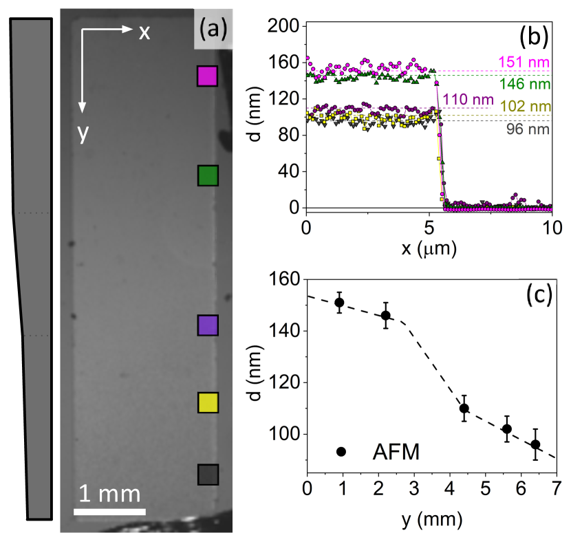
An important first step consists in characterizing the structure of the wedge-shaped films from milimetric down to nanoscopic scales. Fig. 1(a) shows an optical image of the rectangular film with reasonably well-defined edges and the five regions where the thickness variation was investigated, indicated by colored square boxes. Representative thickness profiles obtained from AFM images are presented in panel (b). The thickness values for each region, represented by the colored dashed lines, were evaluated by averaging six different profiles and present standard deviations between 4 nm and 6 nm. To evaluate these Pb thicknesses, we subtract 20 nm referent to the Ge layer. Fig. 1(c) shows the film thickness versus vertical position obtained from the AFM data. The dashed lines are an approximation of the real thickness profile and were used in the numerical simulations. The microstructure and thickness evolution throughout the film are corroborated by SEM images and EDS spectra, as shown in Appendix B.
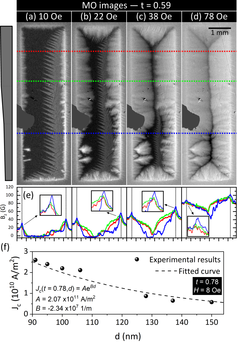
The flux distribution along the gradient film was investigated by MOI, as shown in Fig. 2(a)-(d) at constant temperature = 0.59 and for increasing applied fields after a ZFC procedure. The gray smudge at the left side represents a region where vacuum grease unexpectedly jumped from the cold finger assembly during the experiment. Its gray level was kept constant for all MO images throughout the text. Fortunately, the smudge lies above the MO indicator and does not affect the response of the sample. The flux penetration observed at this temperature is as described by the critical state models Bean (1962, 1964); Kim et al. (1963). In the top thicker half of the sample, the flux front penetrates deeper and becomes more apparent above = 22 Oe. Consequently, its shielding capability is inferior to that of the bottom half (thinner region). In addition, the flux fronts on the left and right borders close to the top and bottom edges are affected as a consequence of the supercurrents which have to adapt to the rectangular geometry of the film, resulting in black diagonal lines, also known as discontinuity lines or d-lines Schuster et al. (1996). The vertical d-line emerges gradually when the field reaches the center of the film, even though the flux front depth is not homogeneous and the full penetration field is not unique. The panels (a)-(d) of Fig. 2 were selected to highlight the difference among the thicker and the thinner regions of the specimen. The fact that we do not observe additional symmetrical d-lines anywhere in the film Motta et al. (2014); Valerio-Cuadros et al. (2021) is a strong indication that there exists a smooth thickness gradient, as represented in Fig. 1(c). It is important mentioning that two flourishing patterns on the bottom left edge are due to defects which favor the flux penetration around them Brisbois et al. (2016) and produce a minor distortion of the central d-line and a slight asymmetry of the side borders. This type of non-uniform flux penetration due to a thickness variation has been also observed in a V3Si film Pinheiro et al. (2019). Fig. 2(e) shows examples of the spatial profile of the induction component taken for different applied fields, being obtained from an average of 208 m wide strip around the colored horizontal dashed lines depicted in panel (a)-(d). They present the typical critical state-like profile for different fields, showing the flux penetration progression for each region. The zigzag patterns, mainly on the right half of the sample, are due to domain boundaries in the MO indicator and have little effect on the flux distribution in the superconducting film. They also become visible as an asymmetry between the peaks on the left and the right edges and in the shielded portion in the flux-free Meissner region up to 38 Oe. Furthermore, the blue line shows a less pronounced penetration due to the thinner local thickness.
This penetration pattern is a consequence of the thickness-dependent current density distribution, which causes a higher current density to flow in the thinner region. In order to crudely estimate the critical current density () at different vertical positions, the flux front penetration depth may be evaluated using MO images. Considering the Bean model Bean (1962, 1964) for uniform thin films with stripe geometry, is given by Brandt et al. (1993); Zeldov et al. (1994):
| (4) |
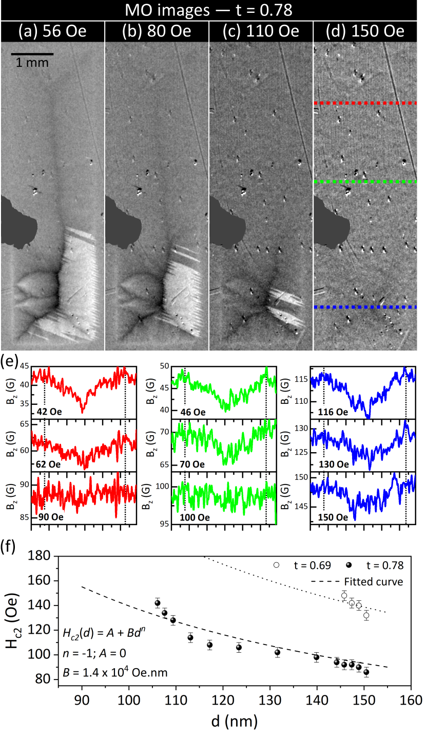
where is the flux front penetration depth measured from the long edges. An example of this estimation is given in Fig. 2(f) for 0.78 and 8 Oe. The thickness dependence described by Equation (4) arises from geometrical considerations for an infinitely long stripe Zeldov et al. (1994). However, this equation does not explicitly take into account the thickness dependence on . For this reason, we have empirically approximated by an exponentially decaying function of film thickness. This behavior was also reported by Foltyn et al. for YBCO Foltyn et al. (1993) and Huebener and Seher for Pb Huebener and Seher (1969), but in those cases for uniform films, each with a different thickness. Therefore, decreasing the thickness makes the superconducting film more capable of self-shielding Poole-Jr et al. (2007); Zeldov et al. (1994). The contrast in MO images is a consequence of the penetrated flux and supercurrent density distributions throughout the superconductor Jooss et al. (2002). Thus, when the superconductor undergoes a phase transition to the normal state, no contrast throughout the image can be recognized. Hence, the critical temperature was determined by MOI in a temperature sweep at zero field after a field cooled (FC) procedure at = 20 Oe. For the wedge-shaped film, the image contrast vanishes homogeneously (not shown) at a single , since there is no significant thickness dependence of in the investigated range (90 nm – 154 nm) for Pb films Strongin et al. (1970); Ivry et al. (2014). Alternatively, the specimen can also undergo a transition to the normal state above the upper critical field () at a certain temperature. Fig. 3(a)-(d) show MO images taken at = 0.78 for applied fields higher than the full penetration field throughout the film after a ZFC procedure. One can observe that the thicker region of the specimen fades out when compared to the thinner part. In panel (a), four current domains are separated by two V-shaped d-lines in the extremes and a nearly vertical d-line in the center of the film. At 80 Oe [panel(b)], the borders of the upper part of the sample practically vanish, but the top V-shaped d-line can still be barely discerned together with the vertical one. At a higher field (110 Oe), one can distinguish the persistence of the superconducting state (below the smudge) thanks to the flux distribution and the d-lines. The evolution of these upper d-lines can be seen in panel (d), taken at 150 Oe, where a X-shaped d-line can still be recognized. These observations demonstrate that the upper critical field depends inversely on the film thickness and reinforces the role played by the thickness variation on the superconducting properties of thin films.
To obtain curves at different temperatures, flux density profiles along the sample width were analyzed for several thicknesses. Fig. 3(e) shows examples of the spatial profile of for different fields, being obtained from an average on a 208 m wide strip around the colored horizontal dashed lines depicted in panel (d). At low fields, the Bean-like profile can be recognized for all regions despite restrictions related to the experimental uncertainty that has a standard deviation of 4 G Chaves et al. (2021). As the applied field is increased, the profile becomes flatter, however, a slope towards the center of the sample can still be perceived. When the upper critical field is reached, a roughly position-independent profile takes place as, for instance, in the red and green profiles for 90 Oe and 100 Oe, respectively. By identifying at different thicknesses, a curve of the upper critical field versus thickness can be plotted. Fig. 3(f) shows the taken from the MO images at reduced temperatures of 0.69 and 0.78. In the former (open circles), only the thicker region of the sample undergoes a transition to the normal state. At = 0.78, . A similar behavior was also observed for uniform-thickness Pb films Harper and Tinkham (1968); Tinkham (1963) and for films made from other metals and alloys Cody and Miller (1968); Harper and Tinkham (1968); Takayama et al. (1971); Brandt et al. (1971).
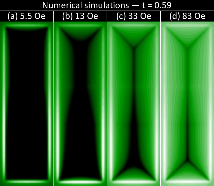
In order to further analyze the experimental MO results, we have simulated a wedge-shaped superconducting film using the TM model framework Denisov et al. (2006b); Vestgården et al. (2011), considering the experimental profile presented in Fig. 2(f). Fig. 4 presents the distribution of magnetic flux density at (a) 5.5 Oe, (b) 13 Oe, (c) 33 Oe, and (d) 83 Oe. The substrate temperature was kept at = 0.59. In this case, regions where magnetic flux is absent appear as black, whereas maximum field corresponds to the brightest intensity. The main features observed experimentally in Fig. 2 are captured by the numerical simulations. In the thicker region on the upper edge, the flux front penetrates deeper and reaches the sample center at around 20 Oe. The flux front in the bottom region, where the supercurrent density is higher, achieves the condition of full penetration at 55 Oe, presenting a better shielding, as in the experiments.
Another interesting feature is the inhomogeneous brightness along the perimeter of the sample. The lower region of the rim is brighter due to a better shielding ability (higher ), leading to a higher concentration of magnetic flux at the edges. This increase in the brightness along the bottom rim of the sample is also observed for the MO images, which can be observed in the zoom of the profiles close to the edges in Fig. 2(e).
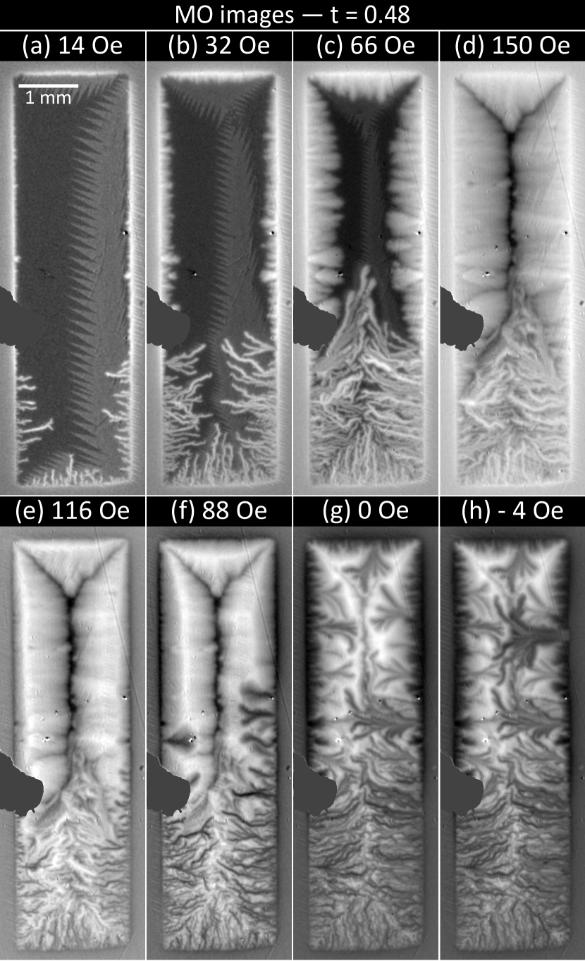
Besides the described smooth flux penetration, when the magnetic diffusion is faster than the thermal diffusion, thermomagnetic instabilities may develop and cause flux avalanches Mints and Rakhmanov (1981). This abrupt penetration regime should also be affected by the thickness gradient. Precisely, it corroborates the previous analysis of distribution throughout the specimen, where one expects to trigger more flux avalanches along the edges with higher Menghini et al. (2005); Colauto et al. (2020). Fig. 5 shows a series of MO images taken at = 0.48 after a ZFC procedure and slowly increasing the applied field up to 150 Oe and then decreasing it to negative values. For increasing fields, the penetration pattern is non-uniform as flux avalanches are nucleated in the thinner region only, whereas from the upper thicker part the penetration is smooth. It is somehow similar to the intriguing effect observed by Albrecht et. al. Albrecht et al. (2007) for a MgB2 film grown onto a vicinal substrate, which results in a current anisotropy of 6% among the edges. Numerical simulations using TM model also presented such avalanche preferential propagation Jing et al. (2016) for different current anisotropies. This phenomenon also appears for the wedged-shaped film, which has a difference of around 400% in between the thinner and thicker regions.
The morphology of the flux avalanches depends strongly on the temperature, as reported by several authors Johansen et al. (2002); Welling et al. (2004); Menghini et al. (2005); Vestgården et al. (2011); Vestgarden et al. (2013); Vestgården et al. (2013). Our results show that even for a fixed temperature, but under different conditions of and modulated by the thickness variation, the morphology of the avalanches depends on thickness. Fig. 5(a) shows the first avalanches nucleated exclusively at the thinner region of the sample, where is higher. In this case, the dendrites present many long and thin fingerlike patterns, almost without ramifications. At 32 Oe, branched medium-sized dendrites for thicknesses around 105 nm (2 mm above the bottom edge) and new longer fingers at the lower part emerged. For an applied field of 66 Oe, even larger and more branched dendrites occur whereas the thicker part develops the critical state-like penetration. Another important feature of the avalanches in panel (c) is their size and the bending of their ramifications toward the thicker zone. In other words, when a region of the sample has no avalanches yet, the first branches point towards the center of the sample, as expected. However, avalanches triggered at higher fields close to the thicker zone deviate and propagate towards the flux-free Meissner region. A possible explanation for this effect relies on the fact that avalanches avoid crossing the existing ones, as described earlier by Johansen et al. Johansen et al. (2001), and there is still flux-free area in the thicker region, while the thinner region is already filled with previously triggered flux avalanches. Similar behavior has also been observed in a work by Choi and coauthors Choi et al. (2008) in which avalanches bend around a gold rim covering only half of a MgB2 film. Fig. 5(d) illustrates the coexistence of the smooth penetration and the avalanche regimes in a single sample: at the upper half of the film the flux front already reached the full penetration state whereas avalanches keep on developing in the thinner part. In this case, some branches are supplanted by the Bean-like penetration around the grayish spot. It is also important to mention that avalanches are not triggered in the thicker zone as a consequence of the lateral heat diffusion, which is larger for this portion, suppressing the occurrence of avalanches Vestgården et al. (2013) .
Additionally, as the critical current density is thickness dependent, the field needed to trigger avalanches increases for increasing thicknesses, as found by Vestgården and coauthors Vestgarden et al. (2013). Considering the dependency for the wedge-shaped film and that the thicknesses where avalanches occur ranges from 90 nm to 105 nm (a variation of 17%), an important ingredient for the above described avalanche morphology is the flux front penetration depth before its occurrence at each position (or thickness) Vestgården et al. (2013). In other words, the deeper initial penetration produces larger and more branching avalanches.
Contrary to Albrecht et al. Albrecht et al. (2007) findings in MgB2 films with anisotropic pinning, non-uniform flux penetration is hysteretic for decreasing fields after a maximum of 150 Oe, i.e., negative field-polarity avalanches (or anti-avalanches) are triggered throughout all four sample edges and their morphology change between the thinner and thicker parts. In this case, anti-avalanches nucleate and propagate into the film already populated by positive flux trapped by the pinning centers, still leaving an imprint of positive induction field for Pinheiro et al. (2020). Panels (e) through (h) of Fig. 5 show anti-avalanches for 116 Oe, 88 Oe, the remnant state, and -4 Oe, respectively. Fingerlike anti-dendrites are triggered along the thinner edges, whereas medium-sized dendrites are nucleated in the middle of the film where only smooth penetration took place for increasing fields. At the remnant state and -4 Oe, several highly branched anti-dendrites can be seen along all edges, even at the top one, showing an interesting hysteresis in the flux penetration for increasing and decreasing applied magnetic fields.
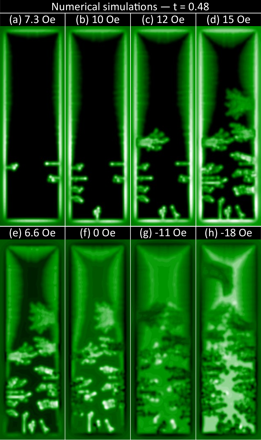
Fig. 6 shows the simulation results for the avalanche regime. At lower fields (7.3 Oe and 10 Oe) after a ZFC procedure, avalanches are triggered in the thinner portion and present a fingerlike shape, whereas at intermediate fields (12 Oe) a branched avalanche is triggered on the left edge. Further avalanches are nucleated at the maximum field of 15 Oe and the Bean-like penetration develops along the upper part of the sample. For decreasing fields, the region out of the sample becomes dark, the field is negative below 6.6 Oe and some small fingerlike anti-dendrites are triggered on the thinner zone at the remnant state. At negative applied fields, additional anti-dendrites with finger shape are nucleated along the thinner region and branched anti-avalanches are also triggered on the thicker region, one of them where the critical state was established previously. Therefore, the overall features of the flux avalanches were confirmed by numerical simulations.
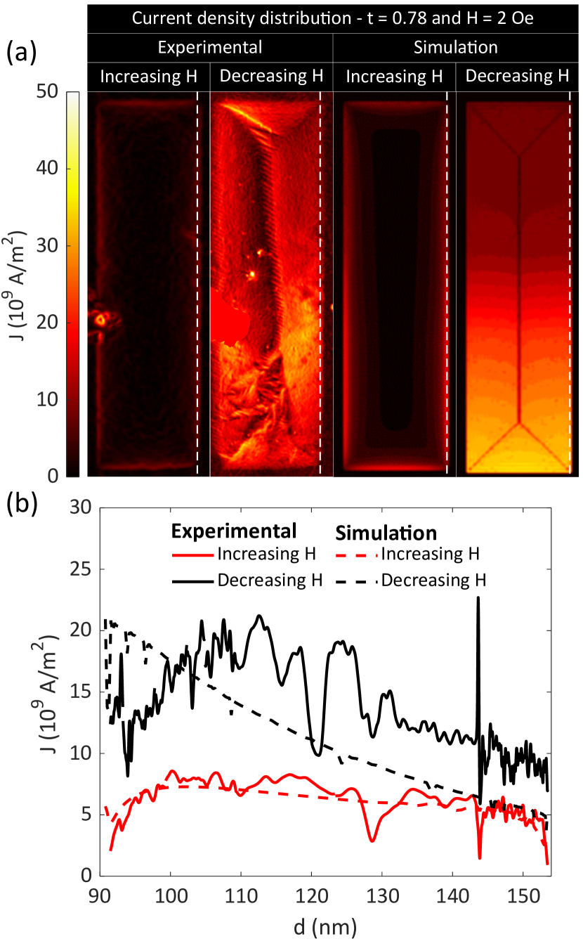
The hysteresis between both branches of applied field for triggering flux avalanches can be explained based on the magnetic properties of type-II superconductors together with the TM model. Fig. 7 shows current maps and profiles acquired from MO images and simulations for the graded-thickness film. The experimental result was obtained after the transformation from to maps calculated using the algorithm proposed by Meltzer and coauthors Meltzer et al. (2017), considering the proper thickness profile shown in Fig. 1(c). Moreover, we chose the MO image taken at = 0.78 and = 2 Oe to minimize artifacts caused by the presence of zigzag domains in the MO indicator. For increasing fields, the shielding current is mainly confined along the perimeter where the magnetic flux is penetrated and decreases towards the center of the sample, as depicted in Fig. 7(a) for both experimental and simulation data. For decreasing fields after a maximum value high enough to reach the full penetration state, a more complex scenario develops because of the flux penetration and the currents throughout the film. Although in the experimental MO image for decreasing fields, garnet domains along the flux front and defects on the edges affect the results, the comparison to numerical calculations yields a satisfactory correspondence for both increasing and decreasing fields.
Fig. 7(b) shows profiles taken along the white vertical dashed line close to the right edge of the sample. The comparison between simulation and experimental data indicate a good agreement despite the large fluctuations observed in the latter. These fluctuations arise from non-uniform flux penetration due to imperfections on the edges. The main observed feature is that both experiment and simulation show an enhancement of the current density at same during the decrease of the applied field. It is important to note that the experimental profiles are obtained directly from the MO images, being not related to the critical state models. This explains the discrepancy between experimental and simulation data for decreasing . For the latter, is bound by the exponential relationship revealed for in Fig. 2(f), as the simulations do not account for an existing dependency.
Based on these profiles, avalanches are triggered in thicker regions for decreasing fields in part as a consequence of a higher local . An important ingredient in this case, is the positive feedback due to Joule heating, which depends strongly on the critical current density Vestgården et al. (2013). This hysteresis in the threshold fields for the occurrence of flux avalanches was firstly described by Qviller et al. Qviller et al. (2010). The main idea is related to the difference between the applied field and the local field close to the edges where avalanches are usually nucleated. Once the field is reduced after a maximum value, the currents close to the edges reverse and reaches a minimum value for a higher value of in this branch when compared to increasing fields, resulting in higher curves for decreasing applied fields. Therefore, the hysteresis between the increasing and decreasing fields for triggering flux avalanches can be completely understood based on the TM model, as well as the regions where avalanches are triggered and their huge diversity in morphology.
IV Conclusions
In summary, we successfully prepared a rectangular wedge-shaped film of Pb employing shadow-mask evaporation. We observed a strong dependency, as the critical current increased by over a factor of four when going from the thicker (154 nm) to the thinner (90 nm) edge. When the upper critical field is reached for a certain thickness, the superconducting region undergoes a transition to the normal state revealed by a constant value of along the width of the film. Moreover, the variation of with thickness promotes a great diversity of flux avalanche patterns at a fixed temperature. Based on quantitative MOI, the hysteresis of profiles for increasing and decreasing applied fields explains the occurrence of antiavalanches in the upper half of the specimen. Taking into account the experimental curve , the numerical simulations based on the TM model presented a consistent correspondence with the experimental results.
These findings show that fabricating wedge-shaped specimens, i.e., exhibiting a thickness gradient, is an interesting strategy to investigate in one and the same sample the material properties dependent on thickness. For superconductors, as well as pinning properties can be modulated with suitable thickness.
Acknowledgements
This work was partially supported by the São Paulo Research Foundation (FAPESP, Grant 2021/08781-8), the National Council for Scientific and Technological Development (CNPq, Grants 433700/2018-1, 431974/2018-7, 316602/2021-3, and 309928/2018-4), and Coordenação de Aperfeiçoamento de Pessoal de Nível Superior – Brasil (CAPES) - Finance Code 001. C. X. and L. J. acknowledge the support by the National Natural Science Foundation of China (Grants No. 11972298). L. J. was supported by the China Scholarship Council. The authors would like to thank Laboratory of Structural Characterization (LCE/DEMa/UFSCar) for grating use of its facilities.
L.B.L.G.P. and L.J. contributed equally to this work.
Appendix A Wedge-film deposition
A new all-metal high vacuum chamber was developed to deposit Pb films employing the conventional thermal evaporation technique Smith (1995) to achieve controllable conditions to grow low melting point metals. Pb films were fabricated by evaporating 99.999% pure lead placed in a tungsten boat onto a Si (100) substrate. A base pressure of 8 x torr is achieced using a liquid-nitrogen cold trap far from the steady substrate holder, which was kept at room temperature. Due to the quick degradation and short lifetime of Pb when exposed to air, a cap layer of Ge was deposited to protect it against oxidation. Throughout the deposition, a quartz crystal microbalance (QCM) based on the OpenQCM project Novaetech S.r.l. (2021) was used to monitor the film thickness during deposition.
To avoid contamination during the film deposition, target metals and substrates were cleaned by chemical wet etching. We prepared the following solutions: HF:HNO3 with volume ratio of 1:1 for Ge; CH3COOH:H2O2 with ratio 1:1 for Pb; and Piranha etch for the Si wafers Walker, P. and Tarn, W. H. (1990).
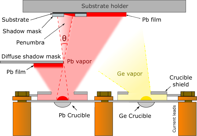
In order to produce a wedge-shaped thin film, a Diffuse-Shadow Mask (DSM) was built and placed inside the chamber between the Pb crucible and the substrate holder, as illustrated in Fig. 8. On the left, the Pb vapor is partially blocked by the crucible shield. The DSM is placed partially covering the Pb crucible, which takes advantage of the non-punctual vapor source to create an area of penumbra identified by and delimited by the dashed red lines delineating the Pb atom paths traced from the extremes of the crucible dip to the substrate holder. Red color indicates the uniform and the wedge-shaped deposition regions for Pb, just below the substrate holder as well as below the DSM. The position of the crucibles in relation to the shields and shutters was made to enable the protective Ge vapor to cover all the wedge-shaped deposition zone. By varying the distance between the DSM and the substrate holder, we are capable of controlling the area of penumbra, i.e., the wedge-shaped deposition zone, and thus change the thickness gradient.
To delineate the edges, another shadow mask was directly clamped to the substrate. Thus, the resulting film has a rectangular shape of area mm2 and the thickness gradient along the major length.
Appendix B SEM/EDS characterization
It is noteworthy that the surface roughness of the Ge layer (the one with which the AFM tip interacts) is uniform all over the sample, showing grains in the nanometric scale, with an average area around 1100 nm2. One can observe this morphology in the secondary electron SEM image in Fig. 9(a), which is somewhat similar to the single Pb layers deposited on different conditions shown in Refs. 95; 96; 97.
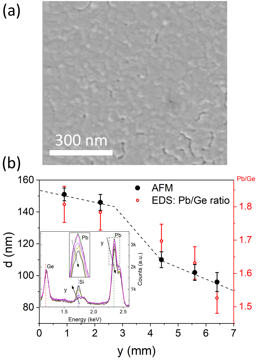
The elemental composition of a given material can be obtained from its EDS spectra Ludwig Reimer (1985). As the detected energy intensity depends on the initial electron beam energy and the average volume of the droplet-shaped interaction region, EDS may also be employed to estimate the film thickness Pascual et al. (1990); Ng et al. (2006); Zhuang et al. (2009); Habiger and Stein (1992); Pinheiro et al. (2019). Most authors use the relation , where () is the peak intensity of the substrate (film), to obtain the thickness. One way to determine is to scan the incident electron beam energy to identify at which value the generation of X-rays is confined only to the sample film Pascual et al. (1990). Then a calibrated curve can be generated from known thicknesses to calculate the thickness of unknown samples. In our case, we kept the acceleration voltage constant at 5 kV, which is large enough to interact with all different layers, including the substrate, and use the Pb/Ge intensity ratio to map the relative profile of the Pb layer along the gradient thickness of the film.
Thus, we chose the same positions where the AFM imaging was performed and monitored the relative heights of the X-ray peaks of the three main elements, assuming that the initial energy of the electron beam penetrates deeply enough to interact with all layers concomitantly. The inset in Fig. 9(b) shows the five spectra for the different regions indicated in Fig. 1(a) in the range of 1.08 to 2.60 keV, where one can identify the Ge-L (1.188 keV), Si-K (1.739 keV), and Pb-M (2.342 keV) characteristic radiation Goldstein et al. (2003); Reed (2005). Since the Ge layer is uniform, its peak height is constant for all vertical positions. As expected, the peak height related to Pb decreases as the thickness decreases, as indicated in the zoom-up in the center of the graph. Conversely, a higher signal due to Si is obtained as the superconducting film becomes thinner as an indication that the electron beam interacts more with the substrate. Black arrows were added to the peaks to indicate the decrease in thickness. In contrast to the previous works cited, we use the intensity peak ratio between Pb/Ge, which is directly proportional to , to represent the relative thickness variation as depicted in the main panel of Fig. 9(b). The error bars were taken as 5% for the Pb/Ge ratio based on the relative error of the element amounts. One can observe that the data follows the general behavior of the thickness determined by AFM despite the different scale. Therefore, this data confirms the general behavior of the non-linear curve for the thickness variation.
References
- Wendin (2017) G. Wendin, Rep. Prog. Phys. 80 (2017).
- Kjaergaard et al. (2020) M. Kjaergaard, M. E. Schwartz, J. Braumüller, P. Krantz, J. I.-J. Wang, S. Gustavsson, and W. D. Oliver, Annu. Rev. Condens. Matter Phys. 11, 369 (2020).
- Hadfield (2009) R. H. Hadfield, Nat. Photonics 3, 696 (2009).
- Natarajan et al. (2012) C. M. Natarajan, M. G. Tanner, and R. H. Hadfield, Supercond. Sci. Technol. 25, 063001 (2012).
- Franssila (2010) S. Franssila, Introduction to Microfabrication, 2nd ed. (Wiley Online Library, 2010) pp. 1–518.
- Luna-Moreno and Monzón-Hernández (2007) D. Luna-Moreno and D. Monzón-Hernández, Appl. Surf. Sci. 253, 8615 (2007).
- Yamamura et al. (2008) K. Yamamura, S. Shimada, and Y. Mori, CIRP Annals 57, 567 (2008).
- Choi et al. (2010) Y.-O. Choi, N.-H. Kim, J.-S. Park, and W.-S. Lee, Mater. Sci. Eng. B 171, 73 (2010).
- Wang et al. (2018) B. Wang, X. Fu, S. Song, H. O. Chu, D. Gibson, C. Li, Y. Shi, and Z. Wu, Coatings 8 (2018).
- Kim et al. (2018) S.-G. Kim, Q. Hu, K.-B. Nam, M. J. Kim, and J.-B. Yoo, Chem. Phys. Lett. 698, 157 (2018).
- Knehr et al. (2021) E. Knehr, M. Ziegler, S. Linzen, K. Ilin, P. Schanz, J. Plentz, M. Diegel, H. Schmidt, E. Il’ichev, and M. Siegel, J. Vac. Sci. Technol. A 39, 052401 (2021).
- Zarnetta et al. (2010) R. Zarnetta, R. Takahashi, M. L. Young, A. Savan, Y. Furuya, S. Thienhaus, B. Maaß, M. Rahim, J. Frenzel, H. Brunken, Y. S. Chu, V. Srivastava, R. D. James, I. Takeuchi, G. Eggeler, and A. Ludwig, Adv. Funct. Mater. 20, 1917 (2010).
- Ludwig (2019) A. Ludwig, npj Comput. Mater. 5, 70 (2019).
- Yuan et al. (2022) J. Yuan, Q. Chen, K. Jiang, Z. Feng, Z. Lin, H. Yu, G. He, J. Zhang, X. Jiang, X. Zhang, Y. Shi, Y. Zhang, M. Qin, Z. G. Cheng, N. Tamura, Y. feng Yang, T. Xiang, J. Hu, I. Takeuchi, K. Jin, and Z. Zhao, Nature 602, 431 (2022).
- Palmisano et al. (2010) V. Palmisano, M. Filippi, A. Baldi, M. Slaman, H. Schreuders, and B. Dam, Int. J. Hydrogen Energy 35, 12574 (2010).
- Hiromasa et al. (2021) S. Hiromasa, O. Takahiro, M. Takumi, and S. Shogo, Frontiers in Nanotechnology 3, 70 (2021).
- Born et al. (2006) F. Born, M. Siegel, E. K. Hollmann, H. Braak, A. A. Golubov, D. Y. Gusakova, and M. Y. Kupriyanov, Phys. Rev. B 74, 140501 (2006).
- Antropov et al. (2013) E. Antropov, M. S. Kalenkov, J. Kehrle, V. I. Zdravkov, R. Morari, A. Socrovisciuc, D. Lenk, S. Horn, L. R. Tagirov, A. D. Zaikin, A. S. Sidorenko, H. Hahn, and R. Tidecks, Supercond. Sci. Technol. 26, 085003 (2013).
- Du et al. (1995) Q. Du, M. D. Gunzburger, and J. S. Peterson, Phys. Rev. B 51, 16194 (1995).
- Chapman et al. (1996) S. J. Chapman, Q. Du, and M. D. Gunzburger, Z. Angew. Math. Phys. 47, 410 (1996).
- Sardella and Brandt (2009) E. Sardella and E. H. Brandt, Supercond. Sci. Technol. 23, 025015 (2009).
- Lu et al. (2016) Y. Lu, Z. Jing, H. Yong, and Y. Zhou, Proc. R. Soc. A 472, 20160469 (2016).
- Sabatino et al. (2012) P. Sabatino, G. Carapella, and M. Gombos, J. Appl. Phys. 112, 083909 (2012).
- Gladilin et al. (2015) V. N. Gladilin, J. Ge, J. Gutierrez, M. Timmermans, J. Van de Vondel, J. Tempere, J. T. Devreese, and V. V. Moshchalkov, New J. Phys. 17 (2015).
- Hengstberger et al. (2010) F. Hengstberger, M. Eisterer, and H. W. Weber, Appl. Phys. Lett. 96 (2010), 1001.1056 .
- Mogro-Campero et al. (1990) A. Mogro-Campero, L. G. Turner, E. L. Hall, N. Lewis, L. A. Peluso, and W. E. Balz, Supercond. Sci. Technol. 3, 62 (1990).
- Foltyn et al. (2003) S. R. Foltyn, P. N. Arendt, Q. X. Jia, H. Wang, J. L. MacManus-Driscoll, S. Kreiskott, R. F. DePaula, L. Stan, J. R. Groves, and P. C. Dowden, Appl. Phys. Lett. 82, 4519 (2003).
- Onori and Rogani (1985) S. Onori and A. Rogani, Physica B+C 132, 217 (1985).
- Chaudhari and Brown (1965) R. D. Chaudhari and J. B. Brown, Phys. Rev. 139, A1482 (1965).
- Il’in et al. (2010) K. Il’in, D. Rall, M. Siegel, A. Engel, A. Schilling, A. Semenov, and H.-W. Huebers, Physica C 470, 953 (2010).
- Talantsev and Tallon (2015) E. F. Talantsev and J. L. Tallon, Nat. Commun. 6, 7820 (2015).
- Brisbois et al. (2017) J. Brisbois, V. N. Gladilin, J. Tempere, J. T. Devreese, V. V. Moshchalkov, F. Colauto, M. Motta, T. H. Johansen, J. Fritzsche, O.-A. Adami, N. D. Nguyen, W. A. Ortiz, R. B. G. Kramer, and A. V. Silhanek, Phys. Rev. B 95, 094506 (2017).
- Bean (1962) C. P. Bean, Phys. Rev. Lett. 8, 250 (1962).
- Kim et al. (1963) Y. B. Kim, C. F. Hempstead, and A. R. Strnad, Phys. Rev. 129, 528 (1963).
- Fietz et al. (1964) W. A. Fietz, M. R. Beasley, J. Silcox, and W. W. Webb, Phys. Rev. 136, A335 (1964).
- Burger et al. (2019) L. Burger, I. S. Veshchunov, T. Tamegai, A. Silhanek, S. Nagasawa, M. Hidaka, and B. Vanderheyden, Supercond. Sci. Technol. 32, 125010 (2019).
- Jiang et al. (2020) L. Jiang, C. Xue, L. Burger, B. Vanderheyden, A. V. Silhanek, and Y.-H. Zhou, Phys. Rev. B 101, 224505 (2020).
- Motta et al. (2021) M. Motta, L. Burger, L. Jiang, J. D. G. Acosta, Ž. Jelić, F. Colauto, W. A. Ortiz, T. H. Johansen, M. V. Milošević, C. Cirillo, C. Attanasio, C. Xue, A. V. Silhanek, and B. Vanderheyden, Phys. Rev. B 103, 224514 (2021).
- Chaves et al. (2021) D. A. D. Chaves, I. M. de Araújo, D. Carmo, F. Colauto, A. A. M. de Oliveira, A. M. H. de Andrade, T. H. Johansen, A. V. Silhanek, W. A. Ortiz, and M. Motta, Appl. Phys. Lett. 119, 022602 (2021).
- Brandt (1997) E. H. Brandt, Phys. Rev. B 55, 14513 (1997).
- Brandt (1994a) E. H. Brandt, Phys. Rev. B 49, 9024 (1994a).
- Clem and Sanchez (1994) J. R. Clem and A. Sanchez, Phys. Rev. B 50, 9355 (1994).
- Brandt (1994b) E. H. Brandt, Phys. Rev. B 50, 4034 (1994b).
- Zeldov et al. (1994) E. Zeldov, J. R. Clem, M. McElfresh, and M. Darwin, Phys. Rev. B 49, 9802 (1994).
- Altshuler and Johansen (2004) E. Altshuler and T. H. Johansen, Rev. Mod.Phys. 76, 471 (2004).
- Denisov et al. (2006a) D. V. Denisov, D. V. Shantsev, Y. M. Galperin, E. M. Choi, H. S. Lee, S. I. Lee, A. V. Bobyl, P. E. Goa, A. A. Olsen, and T. H. Johansen, Phys. Rev. Lett. 97 (2006a).
- Colauto et al. (2020) F. Colauto, M. Motta, and W. A. Ortiz, Supercond. Sci. Technol. 34, 013002 (2020).
- Yurchenko et al. (2009) V. V. Yurchenko, T. H. Johansen, and Y. M. Galperin, Low Temp. Phys. 35, 619 (2009).
- Vestgården et al. (2018) J. I. Vestgården, T. H. Johansen, and Y. M. Galperin, Low Temp. Phys. 44, 460 (2018).
- Vestgården et al. (2011) J. I. Vestgården, D. V. Shantsev, Y. M. Galperin, and T. H. Johansen, Phys. Rev. B 84, 054537 (2011).
- Blanco Alvarez et al. (2019) S. Blanco Alvarez, J. Brisbois, S. Melinte, R. B. G. Kramer, and A. V. Silhanek, Sci. Rep. 9, 3659 (2019).
- Menghini et al. (2005) M. Menghini, R. J. Wijngaarden, A. V. Silhanek, S. Raedts, and V. V. Moshchalkov, Phys. Rev. B 71, 1 (2005).
- Motta et al. (2014) M. Motta, F. Colauto, J. I. Vestgården, J. Fritzsche, M. Timmermans, J. Cuppens, C. Attanasio, C. Cirillo, V. V. Moshchalkov, J. Van de Vondel, T. H. Johansen, W. A. Ortiz, and A. V. Silhanek, Phys. Rev. B 89, 134508 (2014).
- Abal’osheva et al. (2010) I. Abal’osheva, A. Abal’oshev, M. Cieplak, L. Zhu, and C.-L. Chien, Acta Phys. Pol. A 118, 396 (2010).
- Vestgarden et al. (2013) J. I. Vestgarden, Y. M. Galperin, and T. H. Johansen, “Dendritic flux avalanches in superconducting films of different thickness,” (2013), arXiv:1309.6463 [cond-mat.supr-con] .
- Abaloszewa et al. (2022) I. Abaloszewa, M. Z. Cieplak, and A. Abaloszew, “Thermomagnetic instabilities in Nb films deposited on glass substrates,” (2022), arXiv:2207.12811 [cond-mat.supr-con] .
- Helseth et al. (2001) L. E. Helseth, R. W. Hansen, E. I. Il’yashenko, M. Baziljevich, and T. H. Johansen, Phys. Rev. B 64, 174406 (2001).
- Helseth et al. (2002) L. E. Helseth, A. G. Solovyev, R. W. Hansen, E. I. Il’yashenko, M. Baziljevich, and T. H. Johansen, Phys. Rev. B 66, 1 (2002).
- Shaw et al. (2018) G. Shaw, J. Brisbois, L. B. G. L. Pinheiro, J. Müller, S. Blanco Alvarez, T. Devillers, N. M. Dempsey, J. E. Scheerder, J. Van de Vondel, S. Melinte, P. Vanderbemden, M. Motta, W. A. Ortiz, K. Hasselbach, R. B. G. Kramer, and A. V. Silhanek, Rev. Sci. Instrum. 89, 023705 (2018).
- Thévenaz et al. (1998) P. Thévenaz, U. E. Ruttimann, and M. Unser, IEEE Trans. Image Process. 7, 27 (1998).
- Schneider et al. (2012) C. A. Schneider, W. S. Rasband, and K. W. Eliceiri, Nat. Methods 9, 671 (2012).
- Meltzer et al. (2017) A. Y. Meltzer, E. Levin, and E. Zeldov, Phys. Rev. Applied 8, 064030 (2017).
- Denisov et al. (2006b) D. V. Denisov, A. L. Rakhmanov, D. V. Shantsev, Y. M. Galperin, and T. H. Johansen, Phys. Rev. B 73, 014512 (2006b).
- Mints and Rakhmanov (1981) R. Mints and A. Rakhmanov, Rev. Mod. Phys. 53, 551 (1981).
- Portela et al. (2015) F. S. Portela, L. T. Corredor, P. Barrozo, S.-G. Jung, G. Zhang, J. Vanacken, V. V. Moshchalkov, and J. A. Aguiar, Superconductor Science and Technology 28, 034001 (2015).
- Bean (1964) C. P. Bean, Rev. Mod. Phys. 36, 31 (1964).
- Schuster et al. (1996) T. Schuster, H. Kuhn, and E. H. Brandt, Phys. Rev. B 54, 3514 (1996).
- Valerio-Cuadros et al. (2021) M. I. Valerio-Cuadros, D. A. D. Chaves, F. Colauto, A. A. M. d. Oliveira, A. M. H. d. Andrade, T. H. Johansen, W. A. Ortiz, and M. Motta, Materials 14, 7274 (2021).
- Brisbois et al. (2016) J. Brisbois, O.-A. Adami, J. I. Avila, M. Motta, W. A. Ortiz, N. D. Nguyen, P. Vanderbemden, B. Vanderheyden, R. B. G. Kramer, and A. V. Silhanek, Phys. Rev. B 93, 054521 (2016).
- Pinheiro et al. (2019) L. B. L. G. Pinheiro, M. Motta, F. Colauto, T. H. Johansen, E. Bellingeri, C. Bernini, C. Ferdeghini, and W. A. Ortiz, IEEE Trans. Appl. Supercond. 29, 1 (2019).
- Brandt et al. (1993) E. H. Brandt, M. V. Indenbom, and A. Forkl, Europhys. Lett. 22, 735 (1993).
- Foltyn et al. (1993) S. R. Foltyn, P. Tiwari, R. C. Dye, M. Q. Le, and X. D. Wu, Appl. Phys. Lett. 63, 1848 (1993).
- Huebener and Seher (1969) R. P. Huebener and A. Seher, Phys. Rev. 181, 710 (1969).
- Poole-Jr et al. (2007) C. P. Poole-Jr, H. A. Farach, R. J. Creswick, and R. Prozorov, Superconductivity, second edition ed., Vol. 1 (Academic Press, The Netherlands, 2007) p. 646.
- Jooss et al. (2002) C. Jooss, J. Albrecht, H. Kuhn, S. Leonhardt, and H. Kronmüller, Rep. Prog. Phys. 65, 651 (2002).
- Strongin et al. (1970) M. Strongin, R. S. Thompson, O. F. Kammerer, and J. E. Crow, Phys. Rev. B 1, 1078 (1970).
- Ivry et al. (2014) Y. Ivry, C.-S. Kim, A. E. Dane, D. De Fazio, A. N. McCaughan, K. A. Sunter, Q. Zhao, and K. K. Berggren, Phys. Rev. B 90, 214515 (2014).
- Harper and Tinkham (1968) F. E. Harper and M. Tinkham, Phys. Rev. 172, 441 (1968).
- Tinkham (1963) M. Tinkham, Phys. Rev. 129, 2413 (1963).
- Cody and Miller (1968) G. D. Cody and R. E. Miller, Phys. Rev. 173, 481 (1968).
- Takayama et al. (1971) T. Takayama, T. Ōgushi, and Y. Shibuya, J. Phys. Soc. Jpn. 30, 1083 (1971).
- Brandt et al. (1971) B. L. Brandt, R. D. Parks, and R. D. Chaudhari, J. Low Temp. Phys. 4, 41 (1971).
- Albrecht et al. (2007) J. Albrecht, A. T. Matveev, J. Strempfer, H.-U. Habermeier, D. V. Shantsev, Y. M. Galperin, and T. H. Johansen, Phys. Rev. Lett. 98, 117001 (2007).
- Jing et al. (2016) Z. Jing, H. Yong, and Y. Zhou, Supercond. Sci. Technol. 29, 105001 (2016).
- Johansen et al. (2002) T. H. Johansen, M. Baziljevich, D. V. Shantsev, P. E. Goa, Y. M. G. pe rin, W. N. Kang, H. J. Kim, E. M. Choi, M.-S. Kim, and S. I. Lee, Europhys. Lett. 59, 599 (2002).
- Welling et al. (2004) M. S. Welling, R. J. Westerwaal, W. Lohstroh, and R. J. Wijngaarden, Physica C 411, 11 (2004).
- Vestgården et al. (2013) J. I. Vestgården, D. V. Shantsev, Y. M. Galperin, and T. H. Johansen, “The diversity of flux avalanche patterns in superconducting films,” (2013).
- Johansen et al. (2001) T. H. Johansen, M. Baziljevich, D. V. Shantsev, P. E. Goa, Y. M. Galperin, W. N. Kang, H. J. Kim, E. M. Choi, M. S. Kim, and S. I. Lee, Supercond. Sci. Technol. 14, 726 (2001).
- Choi et al. (2008) E.-M. Choi, V. V. Yurchenko, T. H. Johansen, H.-S. Lee, J. Y. Lee, W. N. Kang, and S.-I. Lee, Supercond. Sci. Technol. 22, 015011 (2008).
- Pinheiro et al. (2020) L. B. Pinheiro, M. Caputo, C. Cirillo, C. Attanasio, T. H. Johansen, W. A. Ortiz, A. V. Silhanek, and M. Motta, Low Temp. Phys. 46, 365 (2020).
- Qviller et al. (2010) A. J. Qviller, V. V. Yurchenko, K. Eliassen, J. I. V. rden, T. H. Johansen, M. R. Nevala, I. J. Maasilta, K. Senapati, and R. C. Budhani, Physica C 470, 897 (2010).
- Smith (1995) D. L. Smith, Thin-Film Deposition: Principles and Practice (McGraw-Hill Education, 1995).
- Novaetech S.r.l. (2021) Novaetech S.r.l., “Quartz crystal microbalance,” https://openqcm.com/openqcm (2021), [Online; accessed 8-December-2021].
- Walker, P. and Tarn, W. H. (1990) Walker, P. and Tarn, W. H., CRC Handbook of Metal Etchants (CRC Press, 1990) p. 1415.
- Perrone et al. (2013) A. Perrone, F. Gontad, A. Lorusso, M. Di Giulio, E. Broitman, and M. Ferrario, Nucl. Instrum. Methods Phys. Res., Sect. A 729, 451 (2013).
- Lorusso et al. (2015) A. Lorusso, F. Gontad, E. Broitman, E. Chiadroni, and A. Perrone, Thin Solid Films 579, 50 (2015).
- Broitman et al. (2016) E. Broitman, F. J. Flores-Ruiz, M. Di Giulio, F. Gontad, A. Lorusso, and A. Perrone, J. Vac. Sci. Technol. A 34, 021505 (2016).
- Ludwig Reimer (1985) Ludwig Reimer, Electron Scattering and Diffusion (Springer, Berlin, Heidelberg, 1985) pp. 1–388.
- Pascual et al. (1990) R. Pascual, L. R. Cruz, C. L. Ferreira, and D. T. Gomes, Thin Solid Films 185, 279 (1990).
- Ng et al. (2006) F. L. Ng, J. Wei, F. K. Lai, and K. L. Goh, Appl. Surf. Sci. 252, 3972 (2006).
- Zhuang et al. (2009) L. Zhuang, S. Bao, R. Wang, S. Li, L. Ma, and D. Lv, in 2009 International Conference on Applied Superconductivity and Electromagnetic Devices (IEEE, 2009) pp. 142–144.
- Habiger and Stein (1992) K. W. Habiger and C. Stein, Thin Solid Films 215, 108 (1992).
- Goldstein et al. (2003) J. I. Goldstein, D. E. Newbury, P. Echlin, D. C. Joy, C. E. Lyman, E. Lifshin, L. Sawyer, and J. R. Michael, Scanning Electron Microscopy and X-Ray Microanalysis, 3rd ed. (Springer Science, New York, 2003).
- Reed (2005) S. J. B. Reed, Electron Microprobe Analysis and Scanning Electron Microscopy in Geology, 2nd ed. (Cambridge University Press, Cambridge, 2005).