Experimental observation of spin–split energy dispersion in high-mobility single-layer graphene/\chWSe2 heterostructures
Abstract
Proximity-induced spin-orbit coupling in graphene has led to the observation of intriguing phenomena like time-reversal invariant topological phase and spin-orbital filtering effects. An understanding of the effect of spin-orbit coupling on the band structure of graphene is essential if these exciting observations are to be transformed into real-world applications. In this research article, we report the experimental determination of the band structure of single-layer graphene (SLG) in the presence of strong proximity-induced spin-orbit coupling. We achieve this in high-mobility hBN-encapsulated SLG/\chWSe2 heterostructures through measurements of quantum oscillations. We observe clear spin-splitting of the graphene bands along with a substantial increase in the Fermi velocity. Using a theoretical model with realistic parameters to fit our experimental data, we uncover evidence of a band gap opening and band inversion in the SLG. Further, we establish that the deviation of the low-energy band structure from pristine SLG is determined primarily by the valley-Zeeman SOC and Rashba SOC, with the Kane-Mele SOC being inconsequential. Despite robust theoretical predictions and observations of band-splitting, a quantitative measure of the spin-splitting of the valence and the conduction bands and the consequent low-energy dispersion relation in SLG was missing – our combined experimental and theoretical study fills this lacuna.
I Introduction
Graphene has attracted much attention due to a plethora of remarkable electronic properties like Dirac energy dispersion, relativistic effects, half-integer quantum Hall effect, and Klein tunneling. Additionally, its van der Waals heterostructures with other 2-dimensional materials [1, 2, 3, 4] host several single-particle and emergent correlated states that are topologically non-trivial [5, 6, 7, 8]. The ability to precisely transfer and align these atomically thin planar structures into high-quality heterostructures promises outstanding opportunities for both fundamental and applied research [9, 10, 11]. This has made theoretical and experimental studies of several aspects of graphene-based van der Waals heterostructures of great contemporary interest [12, 13, 14, 15, 8, 16, 11, 10, 17, 18, 19].
With a long spin-relaxation length of several m at room temperature, graphene appears a perfect base for low-power spintronics devices [20, 21]. However, its extremely weak intrinsic spin-orbit coupling (SOC) strength makes spin manipulation challenging. Decorating the surface of graphene with heavy atoms (such as topological nanoparticles) [7, 22] or weak hydrogenation of graphene [23] improves the SOC in graphene at the cost of introducing disorder and reducing the graphene’s mobility. An alternate technique is interfacing graphene with two-dimensional transition metal dichalcogenides (TMDC) having a high SOC [24, 25, 26, 11, 27, 19, 16, 28, 29, 30, 31, 32, 33, 34, 35, 21].
Before one conceives increasingly complex graphene/TMDC heterostructures and considers their potential applications, it is imperative to understand the impact of the proximity of TMDC on the electronic properties of graphene. Prominent amongst these are the breaking of inversion symmetry, breaking of sub-lattice symmetry, and hybridization of the d-orbitals of the heavy element in TMDC with the p-orbitals of SLG, leading to strong SOC in SLG. This proximity-induced SOC in SLG has three primary components, all of which contribute to spin splitting of the bands – (i) valley-Zeeman (also called Ising) term, which couples the spin and valley degrees of freedom, (ii) Kane-Mele term [36, 37] which couples the spin, valley and sublattice components and opens a topological gap at the Dirac point [18, 38], and (iii) Rashba term [39] which couples the spin and sublattice components.
In the presence of a strong Ising SOC, the electronic band dispersion of graphene is predicted to be spin-split [39, 17, 24, 40, 41, 42], as was observed recently in bilayer graphene/\chWSe2 heterostructures [43, 10]. Consequences of this induced SOC include the appearance of helical edge modes and quantized conductance in the absence of a magnetic field in bilayer graphene [5] and of weak antilocalization [19], and Hanle precession in SLG [44, 45, 46, 27, 47, 48, 44, 28]. Despite these advances, a quantitative study of the effect of a strong SOC on the electronic energy band dispersion of SLG is lacking.
In this research article, we report the results of our studies of quantum oscillations in high-mobility heterostructures of SLG and trilayer \chWSe2. Careful analysis of the oscillation frequencies shows spin-splitting of the order of meV for both the valence band (VB) and the conduction band (CB). We find that the bands remain linear down to at least 70 meV (corresponding to ). Close to zero energy, the lower energy branches of the CB and the VB overlap, leading to band inversion and opening of a band gap in the energy dispersion of SLG. We fit our data using a theoretical model that establishes that, to the zeroth-order, the magnitude of the spin-splitting of the bands and that of the band gap are determined by only the valley-Zeeman and Rashba spin-orbit interactions.
II Results
II.1 Experimental Observations
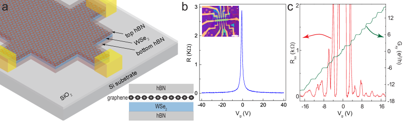
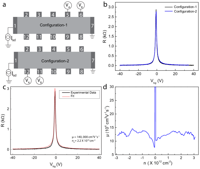
Heterostructures of single-layer graphene and trilayer \chWSe2, encapsulated by hexagonal boron nitride (hBN) (see device schematic Fig. 1(a)) of thickness 20-30 nm, were fabricated using dry transfer technique [49, 50]. One-dimensional Cr/Au electrical contacts were created by standard nanofabrication techniques – note that this method completely evades contacting the \chWSe2 thus avoiding parallel channel transport (see Supplementary Information for details). Electrical transport measurements were performed using a low-frequency ac lock-in technique in a dilution refrigerator at the base temperature of 20 mK unless specified otherwise. Multiple devices of SLG/\chWSe2 were studied, and the data from all of them were qualitatively very similar. All the data presented here are from a device labeled B9S6. The data for two other similar devices are presented in the Supplementary Information. The extracted impurity density from the four-probe resistance of the device as a function of gate voltage (see Fig. 1(b)) was cm-2, and the mobility was 140,000 cm2V-1s-1. The four-probe resistance response as a function of the gate voltage were identical for different measurement configurations (see Supplementary Information), indicating that the fabricated device is spatially homogeneous. Fig. 1(c) shows the quantum Hall data at 3 T – the presence of plateaus at confirms it as SLG. Along with the signature plateaus of SLG, one can see a few of the broken symmetry states appearing already at 3 T, confirming it to be a high-quality device.
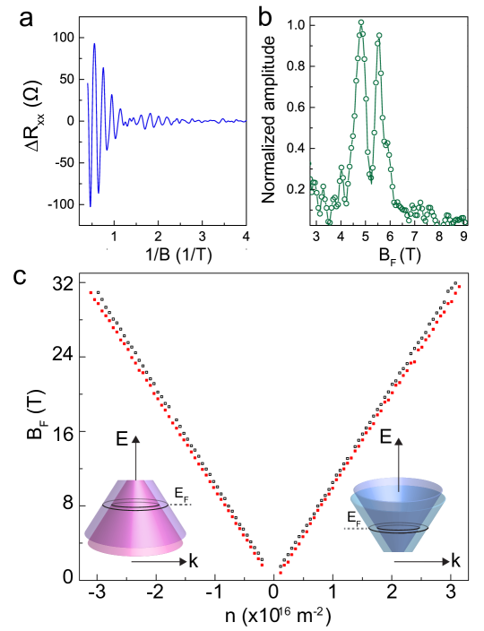
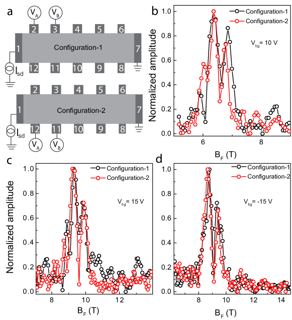
Representative data of the Shubnikov-de Haas (SdH) oscillations measured at 20 mK are plotted in Fig. 2(a). In addition to the expected decay of the amplitude of the oscillations with increasing , we observe the presence of beating, implying two closely spaced frequencies. The fast Fourier transforms (FFT) of the data Fig. 2(b) show that this indeed is the case. We find similar splitting in the SdH oscillation frequency in all the SLG/\chWSe2 devices studied by us – the data for two additional similar devices are presented in the Supplementary Information. There may be a legitimate concern that the observed beating can be caused by device inhomogeneities which lead to different charge carrier density in different regions of the graphene channel. We rule out this artifact from measurements of the four-probe resistance and SdH oscillations in multiple contact configurations – we find that the data are identical in each case (see Supplementary Information).
Recall that the SdH oscillation frequency, is directly related to the cross-sectional area at the Fermi energy by the relation [51]. For an isotropic dispersion in which the Fermi energy is a function of (where are defined with respect to one of the Dirac points, or , of the SLG), the cross-sectional area of the Fermi surface is given by . Fig. 2(c) shows the charge carrier density () dependence of . The appearance of two closely spaced frequencies at all (or ) implies that for each value of the Fermi energy, there are two distinct values of . This is a direct proof of the energy splitting of both the CB and the VB of the SLG.
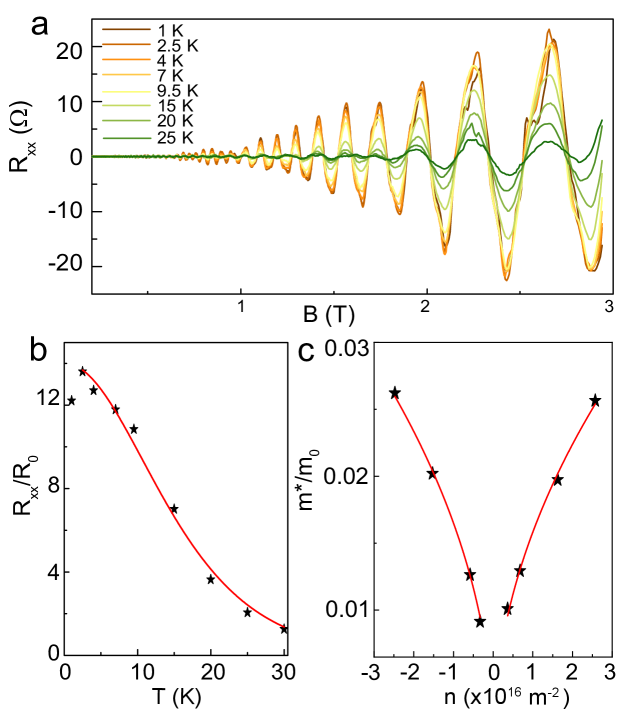
From the temperature dependence of the amplitude of the SdH oscillations (Fig. 3), we extracted the effective charge carrier mass , using the the Lifshitz-Kosevich relation [52, 53]:
| (1) |
Here, the longitudinal resistivity at . On fitting the effective mass versus using the relation [54] (see Supplementary Information), we obtain and Fermi velocity ms-1. The value of being establishes the dispersion relation between energy and momentum in SLG on \chWSe2 to be linear [51].
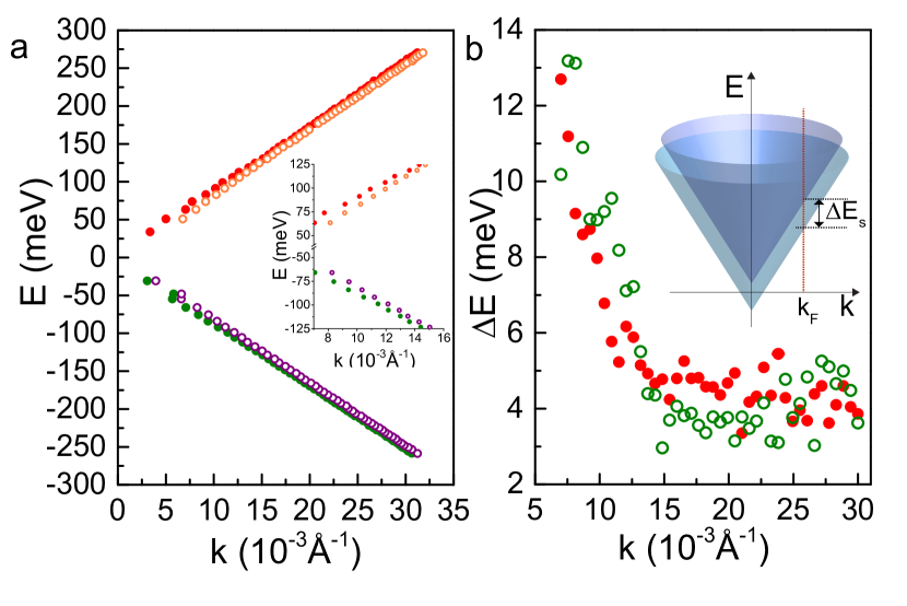
Fig. 4(a) are the resultant plots of versus for both CB and the VB from our experimental data. Note that our experimental data extends down to meV (corresponding to ). Below this number density, the SdH oscillations are not resolvable – presumably due to the dominance of charge puddles on the electrical transport of SLG in this energy range.
We observe that, on extrapolating the plots to , the low-energy branches of the spin-split bands of both the CB and the VB bands enclose a finite area in the -space at . This leads us to expect that there will be an overlap between the lower branches of the CB and VB, ultimately leading to band inversion near the (and ) points. A verification of this assertion requires further measurements in extremely high quality devices that will allow measurements of SdH oscillations near .
To summarize our experimental observations, we have quantified the spin-splitting of the energy bands in SLG in proximity to \chWSe2 and mapped out the dispersion relation of the spin-split bands of SLG. We find that till a certain energy, the dispersion remains linear; below this energy scale, we observe a deviation from linearity.
II.2 Theoretical calculations
Using the experimental data, we fit a theoretical model to obtain the dispersion relation close to the Dirac points. The continuum Hamiltonian near the Dirac points for SLG with WSe2 has the following terms (see, for instance, Ref. [39]):
| (2) | |||||
In Eq. 2, the Pauli matrices and the represent the sublattice and spin degrees of freedom, respectively. The first term denotes the linear dispersion near the Dirac points, where is the Fermi velocity, and are the momenta with respect to the Dirac point, and denotes the valleys () respectively (We note that , where is the nearest-neighbor hopping amplitude and the nearest neighbour carbon carbon distance is 1.42 Å). The second term represents a sublattice potential of strength . We have considered the four possible spin-orbit couplings: (i) Kane-Mele SOC with strength , (ii) valley-Zeeman SOC with strength , (iii) Rashba SOC with strength , and (iv) pseudo-spin asymmetric SOC with strengths and for sublattices A and B respectively.
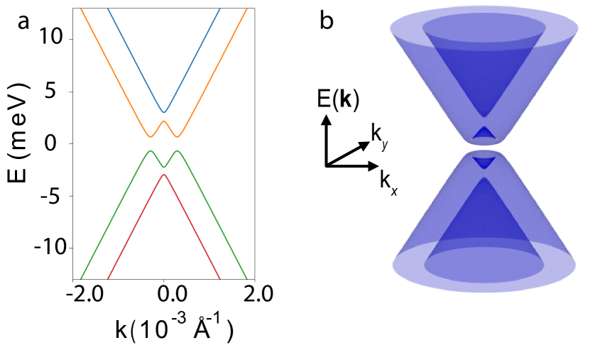
Since this Hamiltonian results in the same dispersion at both the valleys, we only consider the case ( point). The Hamiltonian in Eq. 2 is invariant under a simultaneous rotation of , and by the same angle; this implies that the dispersion is isotropic in momentum space, and it is sufficient to take and . The data for the four bands shown in Fig. 4(a) are fitted to the Hamiltonian with and as the fit parameters. The best fit gives meV implying a large Fermi velocity in this device of ms-1 (compared to about ms-1 in pristine SLG [55]). The parameters in the Hamiltonian which give the spin-split band gap in both conduction and valence bands are and . We find that the best fit gives the values of and to lie on a circle of radius meV, such that
| (3) |
where can take any value from to , and . Eq. 3 can be understood by looking at the first-order perturbative effect of the valley-Zeeman and Rashba terms in the Hamiltonian. Taking and the perturbation we find that the zeroth order spin-degenerate dispersion in the positive and negative energy bands receives first-order corrections given by
| (4) |
for both the bands, thus giving the general relation in Eq. 3. This gives a gap equal to twice meV which fits the experimentally observed value of meV. The two extreme cases are given by with only valley-Zeeman SOC and with only Rashba SOC. The overall magnitude of effective SOC of meV agrees well with previous reports [48, 19, 18, 39].
The band dispersion for higher energies ( meV) remains unaffected for any combination of and which satisfies meV. However, the relative magnitudes of and modifies the lower energy band dispersion ( meV) – a region inaccessible in our experiments. To evaluate the value of and explicitly, one needs the value of the band gap at . As is well known, the presence of finite impurity density ( for this device) leads to the dominance of charge puddles on the electrical transport of SLG at the Dirac point making it extremely difficult to make an accurate estimate of such a small energy gap. In the absence of such information, we take the theoretically predicted value of meV [39] which corresponds to in Eq. 3. This yields the strength of the valley-Zeeman term to be meV and a maximum expected band gap of meV for meV. The resulting dispersion is plotted in Fig. 5(a). In generating this plot, we have used meV, meV, meV and meV [39]. Fig. 5(b) further shows the 3-dimensional plot of the energy dispersion for this model.
III Discussions
Coming to the role of the magnetic field in the extracted energy dispersion relation, the SdH oscillations were studied at a magnetic field of the order of 1 T. This field gives a very small Zeeman energy of the order of meV in the energy. Since the experimental data points are quite far from , we can ignore the magnetic field effect in the Hamiltonian. Further, the fitting does not give us the values of , , , and with any certainty. While the terms do not alter the dispersion in our region of interest, the other two parameters, and will open up a gap at the two values of the energy lying at . The effect of the Kane-Mele term in this model has been further discussed in the Supplementary Information. However, we note that the presence of , , and does not alter the spin-split band gap of 5 meV observed between the bands away from zero energy.
All previous theoretical and experimental studies note that the valley-Zeeman and the Rashba are the major spin-orbit coupling (SOC) terms for graphene/TMDs [48, 19, 18, 39]. These two terms by themselves give a constant energy gap between the spin-split bands. The other relevant spin-orbit coupling terms are and . The terms are negligibly small and do not alter the band dispersion in the region of interest. On the other hand, we find that including a very large and terms meV in the standard theoretical models can give a dispersion where the energy gap between the two spin-split bands increases as one approaches the Dirac point. However, such large and might not be reasonable and have not been reported to date. To the best of our knowledge, there is no consistent theoretical understanding of the increase in energy gap between the spin-split bands on approaching the Dirac point; we leave this as an open question to be explored in near future.
Finally, a comment on the relative magnitudes of and : The spin relaxation mechanism in graphene/TMDC heterostructures is extraordinary. It relies on intervalley scattering and can only occur in materials with spin-valley coupling. In such systems, the lifetime and relaxation length of spins pointing parallel to the graphene plane (, ) can be markedly different from those of spins pointing out of the graphene plane (, ). Realistic modeling of experimental studies indicate that the spin lifetime anisotropy ratio can be as large as a few hundred in the presence of intervalley scattering [44, 47, 41]. Recall that the provides an out-of-plane spin-orbit field and affects the in-plane spin relaxation time, . On the other hand, generates an in-plane spin-orbit field and is relevant for determining [47]. The large spin lifetime anisotropy ratio () seen both from experiments and theory [44, 47, 41] show that the value of can indeed be significantly larger as compared to .
In conclusion, we have experimentally determined the band structure of single-layer graphene in the presence of proximity-induced SOC. We find both the VB and the CB spin-split with a spin-energy gap of meV; the splitting increases as one approaches the Dirac point. There are strong indications of overlap of the lower energy branches of the conduction and the valence bands. We also provide precise values of the spin splitting energy, the Fermi velocity and the effective mass of charge carriers in graphene/WSe2 hetrostructures. Theoretical modeling of the data establishes that the band dispersion near the Dirac point and the magnitude of the spin-splitting are determined primarily by large valley-Zeeman (Ising) SOC and small Rashba SOC. Our work raises the strong possibility that in this system, the transport properties near the Dirac point are dominated by charge carriers of a single spin component, making this system a potential platform for realizing spin-dependent transport phenomena, such as quantum spin-Hall and spin-Zeeman Hall effects.
Methods
Device Fabrication
The SLG, \chWSe2, and hBN flakes were obtained by mechanical exfoliation on \chSiO2/\chSi wafer using scotch tape from the corresponding bulk crystals. The thickness of the flakes was verified from Raman spectroscopy. Heterostructures of SLG and \chWSe2, encapsulated by single-crystalline hBN flakes of thickness 20-30 nm was fabricated by dry transfer technique using a home-built transfer set-up consisting of high-precision XYZ-manipulators. The heterostructure was then annealed at C for 3 hours. Electron beam lithography followed by reactive ion etching (where the mixture of \chCHF3 and \chO2 gas were used with flow rates of 40 sccm and 4 sscm, respectively, at a temperature of 25∘C at the RF power of 60 W) was used to define the edge contacts. The electrical contacts were fabricated by depositing Cr/Au (5/60 nm) followed by lift-off in hot acetone and IPA.
Measurements
All electrical transport measurements were performed using a low-frequency AC lock-in technique in a dilution refrigerator (capable of attaining a lowest temperature of 20 mK and maximum magnetic field of 16 T).
Data availability
The authors declare that the data supports the findings of this study are available within the main text and its supplementary Information. Other relevant data are available from the corresponding author upon reasonable request.
Acknowledgment:
The authors acknowledge fruitful discussions with Saurabh Kumar Srivastav and Ramya Nagarajan and facilities in CeNSE, IISc. AB acknowledges funding from DST FIST program and DST (No. DST/SJF/PSA01/2016-17). DS acknowledges funding from SERB (JBR/2020/000043). K.W. and T.T. acknowledge support from the Elemental Strategy Initiative conducted by the MEXT, Japan (Grant Number JPMXP0112101001) and JSPS KAKENHI (Grant Numbers JP19H05790 and JP20H00354). DSN thanks DST for Woman Scientist fellowship (WOS-A) (Grant No.SR/WOS-A//PM-98/2018).
Competing interests:
The authors declare no Competing Financial or Non-Financial Interests.
Author Contributions
P.T. and A.B. conceived the idea of this research. P.T. and D.S.N. fabricated the devices; P.T., M.K.J. and A.B. performed the measurements; A.U. and D.S. provided theoretical support; K.W and T.T. grew the material; P.T., M.K.J. and A.B. did the experimental data analysis. P.T., A.U. and A.B. co-wrote the manuscript. All authors discussed the results and commented on the manuscript.
Supplementary Materials
Appendix A Device Fabrication and characterization
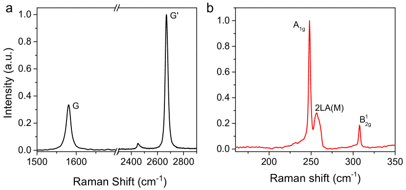
We fabricated heterostructures of single-layer graphene (SLG) and trilayer \chWSe2, encapsulated by single-crystalline hBN flakes of thickness 20-30 nm. The SLG, \chWSe2, and hBN flakes were obtained by mechanical exfoliation on \chSiO2/\chSi wafer using scotch tape from the corresponding bulk crystals. The thickness of the flakes was verified both from optical contrast under an optical microscope and Raman spectroscopy.
The Raman data for SLG and trilayer \chWSe2 flake are shown in Figure. S6(a) and (b) respectively. For the graphene, the high intensity of the Lorentzian G’ peak confirms it to be a single-layer. The flakes were formed into a heterostructure using dry transfer technique [49] using a home-built transfer set-up consisting of high-precision XYZ-manipulators, the entire process being performed under an optical microscope.Briefly, the hBN was first picked up using a Polycarbonate (PC) film at 90oC. This combination was then used to pick up the SLG followed by \chWSe2 and hBN. The prepared stack was transferred on a clean Si/\chSiO2 wafer at 180oC and cleaned using chloroform to remove the PC, and this was followed by cleaning with acetone and isopropyl alcohol.The heterostructure was then annealed at C for 3 hours.
Electron beam lithography was used to define the edge contacts. The edge contacts were made by reactive ion etching (where the mixture of \chCHF3 and \chO2 gas was used with flow rates of 40 sccm and 4 sscm, respectively, at a temperature of 25∘C at the RF power of 60 W) [56]. The electrical contacts were finally created by depositing Cr/Au (5/60 nm) followed by lift-off in hot acetone and IPA. Cr/Au was chosen as it forms a very high quality ohmic contact with graphene [56], but at the same time it does not form any contact with \chWSe2 due to high Schottky barrier and large difference in work functions [57, 58]. Finally, the device was etched into a Hall bar geometry. An optical image of the final device is shown in the main text (inset of Fig. 1(b)).
To estimate the impurity density () and field-effect mobility () of the device, the gate-voltage dependent resistance data were fitted by the equation
| (5) |
where is the contact resistance, and are the channel length and width, respectively, is the capacitance per unit area, and is the value of the back-gate voltage at the Dirac point. Supplementary Figure S7 (b)is the plot of four probe resistance versus gate voltage in two different measurement configurations (see Supplementary Figure S7(a)). One can see that the data for the two contact configurations are identical indicating that there is no local shift in the Dirac point in the graphene channel. This shows that the fabricated device is homogeneous and confirms that the observed beating in the SdH oscillation does not arise from spatial number density inhomogeneity.
Supplementary Figure S7(c) shows the mobility extraction fitting curve (red) using Eq. (5). The extracted was cm-2, and was found to be nearly 140,000 cm2 V-1s-1. Supplementary Figure S7(d) shows a plot of mobility versus charge carrier density (), the data was plotted using the equation , where and is conductivity. One can see that away from the Dirac point, the mobility is nearly independent of .
Appendix B Data for additional measurement configurations and additional devices
We measured the Shubnikov-de Haas oscillations (SdH) in multiple configurations in device B9S6. The frequencies extracted for different configurations via FFT match very well with experimental error bars. The data for two of the configurations are shown in Supplementary Figure S8. In Supplementary Figure S8 (a), the measurement configurations are shown for the data in (b), (c) and (d). The FFT for the SdH oscillation measured at V in the two configurations are shown in (b), (c), and (d) respectively. One can note that the FFT for different configurations give the same result. This establishes that the observed two frequencies in the oscillation are intrinsic to the device and do not originate from spatial inhomogeneity of charge carrier density.
We measured SdH in several devices, the results from all of them were similar. Here, we present the data from two such devices: (1) Device B6S1, which is heterostructure of SLG and single layer \chWSe2 encapsulated in hBN with a graphite back gated and (2) device B6S3, which is an SLG/few-layer-\chWSe2 heterostructure encapsulated by hBN, this device is on \chSiO2. Supplementary Figure S9(a) shows the plot of four-probe resistance as function of at V and 20 mK for the device B6S1, Supplementary Figure S9(b) shows the FFT of the data. The data for device B6S3 measured at V are shown in Supplementary Figure S9(c) and (d) respectively. For both devices we observe clear beating of the SdH oscillations and two frequencies in the FFT.
Appendix C Calculation of the dispersion relation
We extract the effective mass by fitting the normalized amplitude of longitudinal resistivity to the relation [52, 53]:
| (6) |
where is the amplitude of longitudinal resistivity and longitudinal resistivity at zero magnetic fields.
The effective mass can be written as
| (7) | |||||
Using , yields
| (8) | |||||
For and for a linear dispersion of single layer graphene (), we have
| (9) | |||||
One can fit the experimentally obtained dependence of on using the relation [54] keeping and as fitting parameters. The fits to the experimental data shown in main text (Fig. 3(c)) yield and ms-1. The value of is nearly , establishing the dispersion relation between energy and momentum for SLG/\chWSe2 to be linear [51].
Appendix D Theoretical Modelling
The continuum Hamiltonian near the Dirac points used for fitting the experimental data has the following terms,
| (10) | |||||
The best fit gives hopping parameter meV implying a large Fermi velocity in this sample. We further note that the parameters in the Hamiltonian which give the spin-split band gap in both conduction and valence bands are and . The other parameters do not significantly alter the dispersion in the region of experimental data.
We also find that the best fit gives the values of and to lie on a circle of radius meV giving a spin-split band gap of meV, such that
| (11) |
The two extreme cases are given by with only valley-Zeeman SOC and with only Rashba SOC are shown in Supplementary Figure S10. In absence of experimental data to fix , we take the value of from literature and produce a plot for meV and meV as shown in Supplementary Figure S10 (c). The actual dispersion of this sample will have a form very similar to Supplementary Figure S10 (c).
Coming to the effect of the Kane-Mele term on the spin-splitting, Supplementary Figure S11(a) shows that produces a very small energy gap between the spin-split bands, that too only at low-values of momenta . It cannot reproduce the band splitting of meV obtained from the experimental data. The experimentally obtained spin-splitting energy gap of meV can only be obtained by turning on the Valley-Zeeman and/or the Rashba SOC. This is demonstrated in Supplementary Figure S11(b) by interchanging the values of and . One can see that while meV and produces a spin-splitting of about 5 meV, for and meV the splittng is negligibly small away from the Dirac point. This establishes that the energy gap between the spin-split bands is determined by the strength of and , as discussed in the main text.
Interestingly, it is observed from the experimental data that as one approaches Dirac point, the energy gap between the spin-split bands increases. To reproduce this pattern in theoretical model, we need to use significantly large values of and along with the Valley-Zeeman and Rashba SOC. Such large values of and are not reasonable and have not been reported so far; meV from most reports [59, 39]. Thus, although it is tempting to explain the trend of increase in the energy gap between the spin-split bands as one approaches the Dirac point to originate from a large , we refrain from doing so.
References
- [1] A. K. Geim and I. V. Grigorieva. Van der waals heterostructures. Nature, 499(7459):419–425, Jul 2013.
- [2] Bettina V. Lotsch. Vertical 2d heterostructures. Annual Review of Materials Research, 45(1):85–109, 2015.
- [3] Hong Wang, Fucai Liu, Wei Fu, Zheyu Fang, Wu Zhou, and Zheng Liu. Two-dimensional heterostructures: fabrication, characterization, and application. Nanoscale, 6:12250–12272, 2014.
- [4] Xing Zhou, Xiaozong Hu, Jing Yu, Shiyuan Liu, Zhaowei Shu, Qi Zhang, Huiqiao Li, Ying Ma, Hua Xu, and Tianyou Zhai. 2d layered material-based van der waals heterostructures for optoelectronics. Advanced Functional Materials, 28(14):1706587, 2018.
- [5] Priya Tiwari, Saurabh Kumar Srivastav, Sujay Ray, Tanmoy Das, and Aveek Bid. Observation of time-reversal invariant helical edge-modes in bilayer graphene/wse2 heterostructure. ACS Nano, 15(1):916–922, 2020.
- [6] Yuan Cao, Valla Fatemi, Shiang Fang, Kenji Watanabe, Takashi Taniguchi, Efthimios Kaxiras, and Pablo Jarillo-Herrero. Unconventional superconductivity in magic-angle graphene superlattices. Nature, 556(7699):43–50, 2018.
- [7] K Hatsuda, H Mine, T Nakamura, J Li, R Wu, S Katsumoto, and J Haruyama. Evidence for a quantum spin hall phase in graphene decorated with bi2te3 nanoparticles. Science Advances, 4(11):eaau6915, 2018.
- [8] Yuan Cao, Valla Fatemi, Ahmet Demir, Shiang Fang, Spencer L Tomarken, Jason Y Luo, Javier D Sanchez-Yamagishi, Kenji Watanabe, Takashi Taniguchi, Efthimios Kaxiras, et al. Correlated insulator behaviour at half-filling in magic-angle graphene superlattices. Nature, 556(7699):80–84, 2018.
- [9] Kazi Rafsanjani Amin and Aveek Bid. Effect of ambient on the resistance fluctuations of graphene. Applied Physics Letters, 106(18):183105, 2015.
- [10] Priya Tiwari, Saurabh Kumar Srivastav, and Aveek Bid. Electric-field-tunable valley zeeman effect in bilayer graphene heterostructures: Realization of the spin-orbit valve effect. Phys. Rev. Lett., 126:096801, Mar 2021.
- [11] Ahmet Avsar, Jun You Tan, T Taychatanapat, J Balakrishnan, GKW Koon, Y Yeo, J Lahiri, A Carvalho, AS Rodin, ECT O’Farrell, et al. Spin-orbit proximity effect in graphene. Nature communications, 5(1):1–6, 2014.
- [12] Josep Ingla-Aynés, Franz Herling, Jaroslav Fabian, Luis E Hueso, and Fèlix Casanova. Electrical control of valley-zeeman spin-orbit-coupling–induced spin precession at room temperature. Physical Review Letters, 127(4):047202, 2021.
- [13] Juan F Sierra, Jaroslav Fabian, Roland K Kawakami, Stephan Roche, and Sergio O Valenzuela. Van der waals heterostructures for spintronics and opto-spintronics. Nature Nanotechnology, pages 1–13, 2021.
- [14] Klaus Zollner, Martin Gmitra, and Jaroslav Fabian. Swapping exchange and spin-orbit coupling in 2d van der waals heterostructures. Physical Review Letters, 125(19):196402, 2020.
- [15] Klaus Zollner, Marko D Petrović, Kapildeb Dolui, Petr Plecháč, Branislav K Nikolić, and Jaroslav Fabian. Scattering-induced and highly tunable by gate damping-like spin-orbit torque in graphene doubly proximitized by two-dimensional magnet cr 2 ge 2 te 6 and monolayer ws 2. Physical Review Research, 2(4):043057, 2020.
- [16] CK Safeer, Josep Ingla-Aynés, Franz Herling, José H Garcia, Marc Vila, Nerea Ontoso, M Reyes Calvo, Stephan Roche, Luis E Hueso, and Fèlix Casanova. Room-temperature spin hall effect in graphene/mos2 van der waals heterostructures. Nano letters, 19(2):1074–1082, 2019.
- [17] Tarik P Cysne, Jose H Garcia, Alexandre R Rocha, and Tatiana G Rappoport. Quantum hall effect in graphene with interface-induced spin-orbit coupling. Phys. Rev. B, 97(8):085413, 2018.
- [18] Jose H. Garcia, Marc Vila, Aron W. Cummings, and Stephan Roche. Spin transport in graphene/transition metal dichalcogenide heterostructures. Chem. Soc. Rev., 47:3359–3379, 2018.
- [19] Zhe Wang, Dong-Keun Ki, Hua Chen, Helmuth Berger, Allan H MacDonald, and Alberto F Morpurgo. Strong interface-induced spin–orbit interaction in graphene on ws 2. Nature Communications, 6(1):1–7, 2015.
- [20] A. Avsar, H. Ochoa, F. Guinea, B. Özyilmaz, B. J. van Wees, and I. J. Vera-Marun. Colloquium: Spintronics in graphene and other two-dimensional materials. Rev. Mod. Phys., 92:021003, Jun 2020.
- [21] L Antonio Benítez, Williams Savero Torres, Juan F Sierra, Matias Timmermans, Jose H Garcia, Stephan Roche, Marius V Costache, and Sergio O Valenzuela. Tunable room-temperature spin galvanic and spin hall effects in van der waals heterostructures. Nature Materials, 19(2):170–175, 2020.
- [22] Conan Weeks, Jun Hu, Jason Alicea, Marcel Franz, and Ruqian Wu. Engineering a robust quantum spin hall state in graphene via adatom deposition. Phys. Rev. X, 1(2):021001, 2011.
- [23] Jayakumar Balakrishnan, Gavin Kok Wai Koon, Manu Jaiswal, AH Castro Neto, and Barbaros Özyilmaz. Colossal enhancement of spin–orbit coupling in weakly hydrogenated graphene. Nature Physics, 9(5):284–287, 2013.
- [24] Martin Gmitra and Jaroslav Fabian. Proximity effects in bilayer graphene on monolayer : Field-effect spin valley locking, spin-orbit valve, and spin transistor. Phys. Rev. Lett., 119:146401, Oct 2017.
- [25] M Gmitra, S Konschuh, Ch Ertler, C Ambrosch-Draxl, and J Fabian. Band-structure topologies of graphene: Spin-orbit coupling effects from first principles. Phys. Rev. B, 80(23):235431, 2009.
- [26] Bowen Yang, Mark Lohmann, David Barroso, Ingrid Liao, Zhisheng Lin, Yawen Liu, Ludwig Bartels, Kenji Watanabe, Takashi Taniguchi, and Jing Shi. Strong electron-hole symmetric rashba spin-orbit coupling in graphene/monolayer transition metal dichalcogenide heterostructures. Phys. Rev. B, 96:041409, Jul 2017.
- [27] Zhe Wang, Dong-Keun Ki, Jun Yong Khoo, Diego Mauro, Helmuth Berger, Leonid S. Levitov, and Alberto F. Morpurgo. Origin and magnitude of ‘designer’ spin-orbit interaction in graphene on semiconducting transition metal dichalcogenides. Phys. Rev. X, 6:041020, Oct 2016.
- [28] Jinsong Xu, Tiancong Zhu, Yunqiu Kelly Luo, Yuan-Ming Lu, and Roland K. Kawakami. Strong and tunable spin-lifetime anisotropy in dual-gated bilayer graphene. Phys. Rev. Lett., 121:127703, Sep 2018.
- [29] Jose H Garcia, Aron W Cummings, and Stephan Roche. Spin hall effect and weak antilocalization in graphene/transition metal dichalcogenide heterostructures. Nano letters, 17(8):5078–5083, 2017.
- [30] Wei Han, Roland K Kawakami, Martin Gmitra, and Jaroslav Fabian. Graphene spintronics. Nature nanotechnology, 9(10):794–807, 2014.
- [31] Taro Wakamura, Francesco Reale, Pawel Palczynski, Sophie Guéron, Cecilia Mattevi, and Hélène Bouchiat. Strong anisotropic spin-orbit interaction induced in graphene by monolayer ws 2. Physical review letters, 120(10):106802, 2018.
- [32] Talieh S Ghiasi, Josep Ingla-Aynés, Alexey A Kaverzin, and Bart J van Wees. Large proximity-induced spin lifetime anisotropy in transition-metal dichalcogenide/graphene heterostructures. Nano letters, 17(12):7528–7532, 2017.
- [33] Manuel Offidani and Aires Ferreira. Microscopic theory of spin relaxation anisotropy in graphene with proximity-induced spin-orbit coupling. Physical Review B, 98(24):245408, 2018.
- [34] Yunqiu Kelly Luo, Jinsong Xu, Tiancong Zhu, Guanzhong Wu, Elizabeth J McCormick, Wenbo Zhan, Mahesh R Neupane, and Roland K Kawakami. Opto-valleytronic spin injection in monolayer mos2/few-layer graphene hybrid spin valves. Nano letters, 17(6):3877–3883, 2017.
- [35] Talieh S Ghiasi, Alexey A Kaverzin, Patrick J Blah, and Bart J van Wees. Charge-to-spin conversion by the rashba–edelstein effect in two-dimensional van der waals heterostructures up to room temperature. Nano letters, 19(9):5959–5966, 2019.
- [36] C. L. Kane and E. J. Mele. Quantum spin hall effect in graphene. Phys. Rev. Lett., 95:226801, Nov 2005.
- [37] C. L. Kane and E. J. Mele. topological order and the quantum spin hall effect. Phys. Rev. Lett., 95:146802, Sep 2005.
- [38] Stefan Ilić, Julia S. Meyer, and Manuel Houzet. Weak localization in transition metal dichalcogenide monolayers and their heterostructures with graphene. Phys. Rev. B, 99:205407, May 2019.
- [39] Martin Gmitra, Denis Kochan, Petra Högl, and Jaroslav Fabian. Trivial and inverted dirac bands and the emergence of quantum spin hall states in graphene on transition-metal dichalcogenides. Phys. Rev. B, 93(15):155104, 2016.
- [40] Jun Yong Khoo, Alberto F. Morpurgo, and Leonid Levitov. On-demand spin-orbit interaction from which-layer tunability in bilayer graphene. Nano Letters, 17(11):7003–7008, Nov 2017.
- [41] Aron W. Cummings, Jose H. Garcia, Jaroslav Fabian, and Stephan Roche. Giant spin lifetime anisotropy in graphene induced by proximity effects. Phys. Rev. Lett., 119:206601, Nov 2017.
- [42] Martin Gmitra and Jaroslav Fabian. Graphene on transition-metal dichalcogenides: A platform for proximity spin-orbit physics and optospintronics. Phys. Rev. B, 92:155403, Oct 2015.
- [43] JO Island, X Cui, C Lewandowski, JY Khoo, EM Spanton, H Zhou, D Rhodes, JC Hone, T Taniguchi, K Watanabe, L S Levitov, M P Zaletel, and A F Young. Spin–orbit-driven band inversion in bilayer graphene by the van der waals proximity effect. Nature, 571(7763):85–89, 2019.
- [44] S. Omar and B. J. van Wees. Spin transport in high-mobility graphene on substrate with electric-field tunable proximity spin-orbit interaction. Phys. Rev. B, 97:045414, Jan 2018.
- [45] Manuel Offidani, Mirco Milletarì, Roberto Raimondi, and Aires Ferreira. Optimal charge-to-spin conversion in graphene on transition-metal dichalcogenides. Phys. Rev. Lett., 119:196801, Nov 2017.
- [46] Johannes Christian Leutenantsmeyer, Josep Ingla-Aynés, Jaroslav Fabian, and Bart J. van Wees. Observation of spin-valley-coupling-induced large spin-lifetime anisotropy in bilayer graphene. Phys. Rev. Lett., 121:127702, Sep 2018.
- [47] L. Antonio Benítez, Juan F. Sierra, Williams Savero Torres, Aloïs Arrighi, Frédéric Bonell, Marius V. Costache, and Sergio O. Valenzuela. Strongly anisotropic spin relaxation in graphene–transition metal dichalcogenide heterostructures at room temperature. Nature Physics, 14(3):303–308, Mar 2018.
- [48] Simon Zihlmann, Aron W. Cummings, Jose H. Garcia, Máté Kedves, Kenji Watanabe, Takashi Taniguchi, Christian Schönenberger, and Péter Makk. Large spin relaxation anisotropy and valley-zeeman spin-orbit coupling in /graphene/-bn heterostructures. Phys. Rev. B, 97:075434, Feb 2018.
- [49] Filippo Pizzocchero, Lene Gammelgaard, Bjarke S Jessen, José M Caridad, Lei Wang, James Hone, Peter Bøggild, and Timothy J Booth. The hot pick-up technique for batch assembly of van der waals heterostructures. Nature Communications, 7(1):1–10, 2016.
- [50] Lei Wang, I Meric, PY Huang, Q Gao, Y Gao, H Tran, T Taniguchi, Kenji Watanabe, LM Campos, DA Muller, et al. One-dimensional electrical contact to a two-dimensional material. Science, 342(6158):614–617, 2013.
- [51] Kostya S Novoselov, Andre K Geim, Sergei Vladimirovich Morozov, Dingde Jiang, Michail I Katsnelson, IVa Grigorieva, SVb Dubonos, and AA Firsov. Two-dimensional gas of massless dirac fermions in graphene. nature, 438(7065):197–200, 2005.
- [52] Carolin Küppersbusch and Lars Fritz. Modifications of the lifshitz-kosevich formula in two-dimensional dirac systems. Phys. Rev. B, 96(20):205410, 2017.
- [53] IM Lifshitz and AM Kosevich. Theory of magnetic susceptibility in metals at low temperatures. Sov. Phys. JETP, 2(4):636–645, 1956.
- [54] AH Castro Neto, Francisco Guinea, Nuno MR Peres, Kostya S Novoselov, and Andre K Geim. The electronic properties of graphene. Rev. Mod. Phys., 81(1):109, 2009.
- [55] Choongyu Hwang, David A Siegel, Sung-Kwan Mo, William Regan, Ariel Ismach, Yuegang Zhang, Alex Zettl, and Alessandra Lanzara. Fermi velocity engineering in graphene by substrate modification. Scientific reports, 2(1):1–4, 2012.
- [56] Lei Wang, I Meric, PY Huang, Q Gao, Y Gao, H Tran, T Taniguchi, Kenji Watanabe, LM Campos, DA Muller, J Guo, P Kim, J Hone, K L Shepard, and C R Dean. One-dimensional electrical contact to a two-dimensional material. Science, 342(6158):614–617, 2013.
- [57] Christopher M Smyth, Rafik Addou, Stephen McDonnell, Christopher L Hinkle, and Robert M Wallace. Wse2-contact metal interface chemistry and band alignment under high vacuum and ultra high vacuum deposition conditions. 2D Materials, 4(2):025084, 2017.
- [58] Yangyang Wang, Ruo Xi Yang, Ruge Quhe, Hongxia Zhong, Linxiao Cong, Meng Ye, Zeyuan Ni, Zhigang Song, Jinbo Yang, Junjie Shi, et al. Does p-type ohmic contact exist in wse 2–metal interfaces? Nanoscale, 8(2):1179–1191, 2016.
- [59] Jose H Garcia, Marc Vila, Aron W Cummings, and Stephan Roche. Spin transport in graphene/transition metal dichalcogenide heterostructures. Chemical Society Reviews, 47(9):3359–3379, 2018.