Present address: ]Google Quantum AI, Mountain View, CA, USA
Absence of edge reconstruction for quantum Hall edge channels in graphene devices
Abstract
Electronic edge states in topological insulators have become a major paradigm in physics. The oldest and primary example is that of quantum Hall (QH) edge channels that propagate along the periphery of two-dimensional electron gases (2DEGs) under perpendicular magnetic field. Yet, despite 40 years of intensive studies using a variety of transport and scanning probe techniques, imaging the real-space structure of QH edge channels has proven difficult, mainly due to the buried nature of most 2DEGs in semiconductors. Here, we show that QH edge states in graphene are confined to a few magnetic lengths at the crystal edges by performing scanning tunneling spectroscopy up to the edge of a graphene flake on hexagonal boron nitride. These findings indicate that QH edge states are defined by boundary conditions of vanishing electronic wavefunctions at the crystal edges, resulting in ideal one-dimensional chiral channels, free of electrostatic reconstruction. We further evidence a uniform charge carrier density at the edges, contrasting with conjectures on the existence of non-topological upstream modes. The absence of electrostatic reconstruction of quantum Hall edge states has profound implications for the universality of electron and heat transport experiments in graphene-based systems and other 2D crystalline materials.
Introduction
In 1982, two years after the discovery of the quantum Hall effect [1], B. Halperin predicted the existence of edge states carrying the electron flow along sample periphery [2]. These edge states, which form unidirectional (chiral) ballistic conduction channels, have been pivotal in understanding most of the transport properties of the QH effect [3, 4]. They have served as an extraordinarily versatile platform for a multitude of quantum coherent experiments [5], culminating recently in the evidence of fractional statistics in the fractional QH effect [6] and the possibility of anyon braiding through interferometry [7].
The existence of edge states was initially inferred as a consequence of the boundary conditions imposed by the physical edges on the electron wavefunctions [2]. The energy of the electron states that are condensed into Landau levels increases upon approaching the edge due to the hard-wall boundary conditions, opening new conduction channels –the QH edge channels– spatially located at their intersection with the Fermi level [2] (see Fig. 1B-C). Inclusion of a smooth electrostatic confining potential, which is experimentally used to define edges in 2DEGs buried in semiconductor heterostructures, enriches the picture with the concept of edge reconstruction [8]. There, the Coulomb interaction energy dominates the confining potential, leading to a transformation of the edge states into a series of wide compressible channels separated by incompressible strips. In the opposite case of a sharp potential, the Coulomb interaction is not relevant and the single particle picture is valid. Edge reconstruction mechanisms have further proven to be of paramount importance in the fractional QH regime where additional co- and/or counter-propagative or even neutral modes [9, 10, 11] can emerge and complexify charge and heat transport [12, 13, 14].
Non-reconstructed edge states can substantially clarify QH edge transport with virtually ideal one-dimensional edge states [19] and new regimes of intra- and inter-channel interactions. Contrary to semiconductor heterostructures, two-dimensional crystalline materials like graphene, for which physical edges are crystal edges, may be archetypical systems hosting such edge states. For graphene and its massless, linear band structure, QH edge states without confining electrostatic potential are expected to be the exact eigenstates of the Dirac equations derived with vanishing boundary conditions at the armchair or zigzag edge [15, 16, 17]. Akin to Halperin’s original prediction [2], these solutions for edges states are maximally confined to a few magnetic lengths ( is the reduced Planck constant, the electron charge and the magnetic field) from the crystal edge, leaving no room for edge reconstruction.
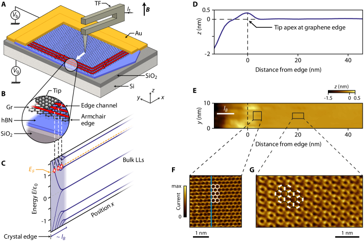
Here, we unveil the real-space structure of the quantum Hall edge states of graphene lying on an insulating hexagonal boron nitride flake (hBN) and evidence the absence of edge reconstruction, by performing scanning tunneling spectroscopy up to the graphene crystal edge, under strong perpendicular magnetic field. We achieved this by overcoming the long-standing experimental challenge [20, 21, 22, 23, 24, 25, 26, 27, 28, 29, 30] of approaching a scanning tunneling tip to the edge without crashing it on the insulating substrate that borders the graphene flake, by means of a prior localization of the graphene edge by atomic force microscopy (AFM). We purposely used a home-made hybrid scanning microscope [18] capable of operating alternatively in AFM and scanning tunneling microscopy (STM) mode, thanks to a PtIr STM tip glued onto a piezoelectric tuning fork acting as a force sensor [31, 32] for AFM (see Fig. 1A).
Our sample schematized in Fig. 1A and B consists of a graphene monolayer deposited on a hBN flake sitting on a Si/SiO2 substrate that serves as a back-gate electrode (see Methods). The graphene flake is contacted by a Cr/Pt/Au tri-layer that allows to apply a voltage bias and collect a tunnel current via the STM tip. All experiments presented here are performed at a temperature of 4.2 K and a perpendicular magnetic field of 14 T.
Results
Quantum Hall edge states spectroscopy
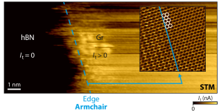
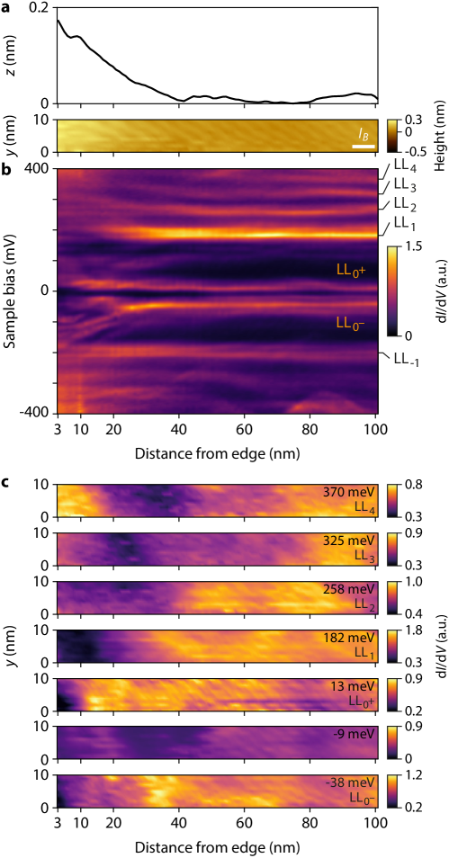
Figure 1E displays a STM topographic image taken in constant current mode to the graphene edge, initially coarsely located by AFM (see Fig. S1). The height profile of this image (Fig. 1D) shows a large flat area, and a slight bump on the left part of the scan. This bump results from the tip-graphene interaction lifting up the graphene edge when the tip is right above it [33]. This bump allows us to locate the edge of the graphene crystal with an accuracy of a few nanometers (see SI). To the left of the bump, the tip dips towards the hBN substrate, on which a tip crash is avoided by a height limit of the STM controller. Atomic scale imaging of the honeycomb lattice shown in Fig. 1F gives insight into the graphene lattice termination. The edge orientation in Fig. 1E, which is reported in Fig. 1F with the blue line, indicates an armchair termination.
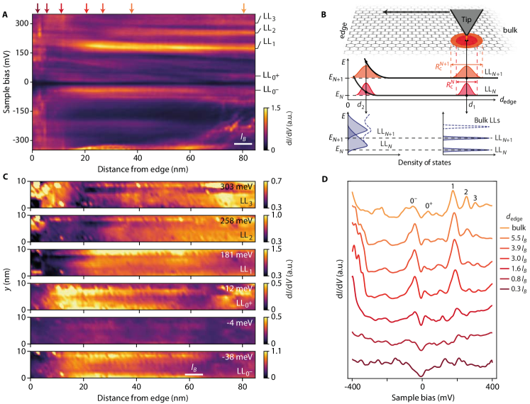
The central result of this work is shown in Figure 2, which presents the evolution of the Landau levels upon approaching the immediate proximity of the graphene edge in the region shown in Fig. 1E, under a magnetic field of 14 T. We first study charge-neutral graphene by tuning the density with the back-gate voltage set at V. Tunneling spectroscopy of Landau levels [34, 35, 36, 37] results in a series of peaks in the tunneling conductance that is proportional to the local density of states. We show in Fig. 2A the tunneling conductance as a function of tip distance perpendicular to the graphene edge , and bias voltage . Far from the edge, Landau levels are readily identified as bright conductance peaks that we label LLN, where is the Landau level index. These conductance peaks are conspicuously stable upon approaching the edge on the left of the figure. Within 40 nm from the edge, we observe a suppression of the Landau level peak heights (see individual spectra in Fig. 2D) starting at distances that depend on the Landau level (the higher the Landau index, the further from the edge). Figure 2C shows spatial maps of the tunneling conductance at the voltage bias of the Landau level peaks. For each Landau level peak, darker areas corresponding to Landau level peak suppression appear further and further from the edge as the Landau level index increases.
These findings contrast with the expectation for a smooth confining potential at the edges, for which the Landau level spectrum would have continuously shifted in energy, following the confining potential as the edge is approached. Since the tunneling conductance probes states on the scale of the electron wavefunction, that is, the cyclotron radius for Landau level index , the suppression of the Landau level peaks, here, reflects a spreading of the spectral weight to higher energy due to an abrupt edge state dispersion at the physical edge, on a very short scale of the order of the magnetic length (see Fig. 2B). This suppression of the tunneling density of states of the Landau levels, which has been observed on graphene on a conductive graphite substrate [28], is therefore direct evidence of QH edge states sharply confined at the edges. Ultimately, on the last few nanometers from the edge, the Landau level peaks disappear completely, and the redistribution of Landau level spectral weight yields a V-shape like tunneling density of states (see Fig. 2D).
In this measurement we have set the Fermi level at charge neutrality, that is, at Landau level filling factor , which leads to a splitting of the zeroth Landau level (see split peaks labeled LL and LL in Fig. 2A) with the opening of an interaction-induced gap at V (see Ref. [18]). This splitting signals the broken-symmetry state [40] at charge neutrality with the Kekulé-bond order [38, 39, 18]. Interestingly, we identified the Kekulé-bond order at 20 nm of the edge in Fig. 1G, indicating that this broken-symmetry state, which develops in the bulk, is robust even in the very proximity of the edge [41].
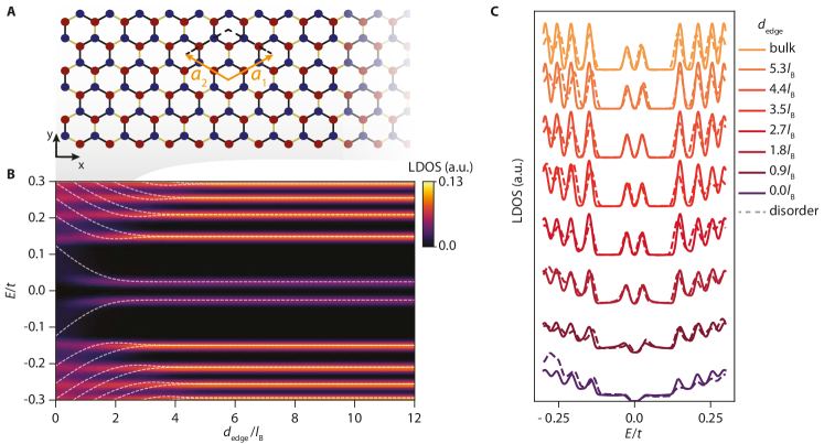
To substantiate our finding we performed numerical simulations of the local density of states of a charge neutral graphene graphene ribbon with an armchair edge under perpendicular magnetic field (see. Fig. 3A) [15, 16, 17].
We computed the Landau levels of the lattice Hamiltonian of nearest-neighbor hopping energy . We assumed a Kekulé-bond order with a gap at half-filling of the zeroth Landau level of mV, as measured experimentally [18]. The eigenstates for a ribbon with periodic boundary conditions along are shown in Fig. 3B as white dashed lines.
The Landau level eigenstates disperse as their average position, locked to their momentum, approaches the physical edge of graphene [42], as schematized in Fig. 1B. Fig. 3B shows the clean local density of states, which integrates the eigenstates weighted by the amplitude of the wavefunctions, as a function of the distance to the edge normalized by , , averaged over each unit cell (see Methods). The range of coincides with the range of displacement in Fig. 2A, allowing direct comparison with the experimental data.
The resulting Landau level peaks are suppressed at higher values of the higher their Landau level index, and on the same spatial scale as observed experimentally in Fig. 2A.
This reduction of spectral weight is more visible in Fig. 3C where we plot spectra for different (solid lines) including a single realization of on-site disorder (dashed lines).
The latter breaks the particle-hole symmetry of the spectrum, and thus may contribute to the asymmetries observed in the zeroth landau level peaks.
On the charge accumulation on the edges
The question of charge carrier homogeneity is critical for graphene transport. A body of work has shown anomalous asymmetry in some transport properties supplemented by scanning probe investigations [43, 44, 45], which points to a charge carrier accumulation at the graphene edges. Its origin may be either electrostatic stray field of the back-gate electrode [46] or chemical doping due to edge treatments (etching) or dangling bonds. In the QH effect, such an accumulation could open up additional counter-propagative edge channels and produce dissipation [46, 44, 45].
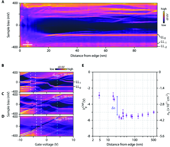
In tunneling experiments, a charge inhomogeneity on the edge would result in an energy shift of the Landau level spectrum as a whole due to a local change of the Landau level filling factor. Our measurements in Fig. 2 provides a first insight on this issue with a remarkable stability of the Landau level peaks in energy that indicates that a possible charge accumulation is not large enough to depin the chemical potential from the zeroth Landau level [18]. In particular, it is lower than the value cm-2 required to fill the zeroth Landau level and reach at 14 T, which would produce a visible energy shift of the Landau level spectrum that we do not observe.
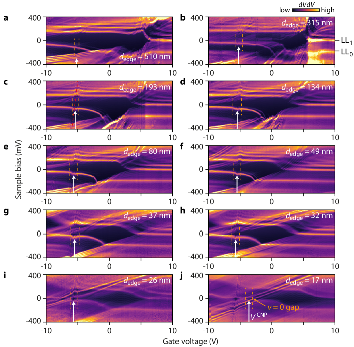
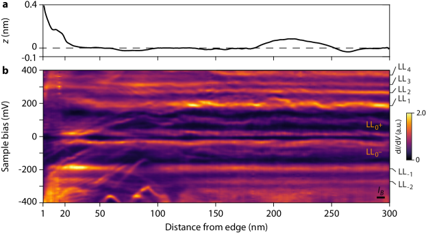
To enhance the sensitivity of the spectroscopy to possible charge inhomogeneities, we performed similar measurements at filling factor ( V), when the Fermi level is pinned by localized states in the cyclotron gap separating LL0 from LL1. There, due to the little density of localized states as compared to the highly degenerate Landau levels, a small variation of charge density would result in a substantial shift of the Landau levels in the tunneling spectra. Figure 4 displays the spatial evolution of the tunneling conductance up to the edge, at and 14 T. As in Fig. 2, the Landau level peaks (LL0, LL-1 and LL-2) stay at the same energy over the scan and vanish at about 20 nm from the edge, clearly indicating the absence of charge accumulation. We further performed systematic gate-tuned tunneling spectroscopy maps at various locations, from 500 nm to 5 nm from the edge (see SI). Figure 4B-D displays three of these maps taken close to the edge. We observe in Fig. 4B the usual staircase pattern of the Landau level peaks due to the successive pinning of the Fermi energy in the Landau levels [47, 48, 18], which allows us to precisely identify the back-gate voltage of the charge neutrality point . As shown in Fig. 4E that displays as a function of the distance from the edge, there is no charge accumulation from 500 nm to 20 nm to the edge, and only within 20 nm of the edge we measure a variation .
Interestingly, such a charge density variation near the edge at 14 T yields a little variation of local filling factor, which would have no consequence on the QH edge transport properties. Extrapolating at lower field, however, would be reached at a magnetic field of 3 T, thus potentially affecting edge transport with additional modes. Yet, the very small spatial scale of this charge accumulation cannot explain recent scanning probes experiments evidencing indirect, sometimes out-of-equilibrium responses within hundreds of nanometers from the edge [44, 45]. We conjecture that this charge accumulation in our particular case is related to the tip-graphene interaction when the tip reaches and lift up the graphene edge (see Supplementary Section III).
Discussion
The issue of charge accumulation on the edge and the ensuing emergence of upstream modes [44, 45] were put forth as an alternative interpretation [49] for the signature of helical edge transport in charge-neutral graphene [50, 51]. Although we cannot exclude that the stray field of the back gate electrode may accumulate charges at high back-gate voltages, that is, away from charge neutrality point, and over a long distance [46], our results show that this accumulation is absent at low back-gate voltage, thus invalidating the doubts raised [49] on the existence of the quantum Hall topological insulator phase in charge neutral-graphene [50, 51]. Still, it may be interesting to revisit non-local transport in non-linear regime [49] in view of the exact spatial structure of the QH edge states in graphene.
Regarding edge reconstruction, a wealth of fractional and integer quantum Hall states exhibit complex sequences of reconstructed edge channels, including additional integer and/or fractional as well as neutral modes [9, 10, 11]. Whereas the smooth electrostatic potential in GaAs and other semiconductors reconstructs edge states into wide compressible stripes of the order of nm (see Ref. [29]), the graphene QH edge states confined on a very short length scale, at few magnetic lengths on the physical edge, pose new constraints and limits for such a reconstruction, opening the investigation of universal transport and thermal properties [19]. Moreover, in such a strongly confined configuration, an enhancement of inter-edge-states interactions can be expected, which makes the picture of independent chiral channels irrelevant in this case, thus impacting charge and heat equilibration [52, 53, 54]. This should impact QH interferometry [55] in graphene systems [56, 57] and other coherent experiments [5], for which the independence, exact positions and nature of edge modes are crucial parameters to address anyon physics as well as other interaction-driven phenomena, such as charging effects [58], spin-charge separation [59] or electron pairing [60].
Note: A very recent work (https://arxiv.org/abs/2210.01831) reports a complementary tunneling spectroscopy study of electrostatically-defined QH edge states at a junction.
methods
Sample fabrication
The graphene/hBN heterostructure was assembled from exfoliated flakes with the van der Waals pick-up technique using a polypropylene carbonate (PPC) polymer [61]. The stack with graphene on top of the hBN flake was deposited using the method described in Ref. [62] on a highly p-doped Si substrate with a nm thick SiO2 layer. Electron-beam lithography using a PMMA resist was used to pattern a guiding markerfield on the whole mm2 substrate to drive the STM tip toward the device and to locate the graphene edge. Cr/Pt/Au electrodes contacting the graphene flake were also patterned by electron-beam lithography and metalized by e-gun evaporation. The sample was thermally annealed at C in vacuum under an halogen lamp to remove resist residues and clean graphene, before being mounted into the STM where it was heated in situ during the cooling to K.
Measurements
Experiments were performed with a home-made hybrid scanning tunneling microscope (STM) and atomic force microscope (AFM) operating at a temperature of K in magnetic fields up to T. The sensor consists of a hand-cut PtIr tip glued on the free prong of a tuning fork, the other prong being glued on a Macor substrate. Once mounted inside the STM, the tip is roughly aligned over the sample at room temperature. The AFM mode was used first for coarse navigation at K on the sample surface to align the tip onto graphene and then for locating coarsely the graphene edge, see SI. The STM imaging in constant-height mode of the edge, done subsequently, yields a fine identification. Scanning tunneling spectroscopy (STS) was performed using a lock-in amplifier technique with a modulation frequency of Hz and rms modulation voltage between mV depending on the spectral range of interest. Current Imaging Tunneling Spectroscopy (CITS) measurements were acquired by starting far from the edge, with a grid whose slow -axis is perpendicular to the edge direction (as imaged by STM) and the -axis is parallel to the edge with a size of a few tens of nanometers. A safety condition is added to the tip vertical -position controller to prevent the crashing into the hBN flake beyond the graphene edge : if the -position reaches a threshold (typically nm below the -position of the tip estimated close to the edge), the tip is withdrawn and the CITS ends. Imaging of the Kekulé-bond order was carried out in STM constant-height mode after tuning the graphene to charge neutrality with the back gate, at a bias voltage corresponding to the energy of the LL peak (see Ref. [18] for details).
Theoretical simulations
To compute the local density of states shown in Fig. 3 we use the simulation software Kwant [63]. First we create a honeycomb lattice in a square system of size , in units of graphene’s lattice constant . The unit-cell for the Kekulé order is tripled compared to pristine graphene, and is defined by the reciprocal vectors and , see Fig. 3A. To calculate the local density of states at a given energy and Kekulé unit cell , we average over the six sites weighted by the corresponding wave-function, , where runs over the six unit cell sites. We compute the local density of states spectra, shown in Fig. 3B as a colormap, using the kernel polynomial method [64] with a target energy resolution of , and a magnetic field of in units of the magnetic flux . The dashed line spectra of Fig. 3B maps are obtained for a finite nano-ribbon of width , with an arm-chair edge parallel to the direction, as in Ref. [42]. We allow the edge to be mis-aligned with the Kekulé lattice vectors, as observed experimentally in Fig. 1F and G. Lastly, the solid lines in Fig. 3C show cuts of the local density of states spectra show in Fig. 3B. The dashed lines are calculated adding a single disorder realization obtained by adding a random on-site potential at each site to the clean local density of states spectra described above. The disorder strength at each site is drawn from a uniform distribution in the interval with .
Data availability
All data needed to evaluate the conclusions in the paper are present in the paper and/or the Supplementary Materials.
Acknowledgments
We thank C. Déprez, B. Halperin, M. Feigelman, M. Goerbig, M. Guerra, D. Perconte, H. Vignaud, and W. Yang for valuable discussions. We thank F. Blondelle, D. Dufeu, Ph. Gandit, D. Grand, G. Kapoujyan, D. Lepoittevin, J.-F. Motte and P. Plaindoux for technical support in setting up of the experimental system. Samples were prepared at the Nanofab facility of the Néel Institute. This work has received funding from the European Union’s Horizon 2020 research and innovation program ERC grants QUEST No. 637815 and SUPERGRAPH No. 866365, and the Marie Sklodowska-Curie grant QUESTech No. 766025. A. G. G. acknowledges financial support by the ANR under the grant ANR-18-CE30-0001-01 (TOPODRIVE).
Author contributions
AC fabricated the sample and performed the measurements. AC, AGG, CR, HS and BS analysed the data. AGG and CR conducted the theoretical analysis. LV assembled the STM microscope. KW and TT supplied the hBN crystals. FG provided technical support on the experiment. BS conceived and supervised the project, designed the experimental set-up, and wrote the paper with inputs from all co-authors.
Competing Interests
The authors declare that they have no competing financial interests.
References
References
- Von Klitzing et al. [1980] K. Von Klitzing, G. Dorda, and M. Pepper, New Method for High-Accuracy Determination of the Fine-Structure Constant Based on Quantized Hall Resistance, Phys. Rev. Lett. 45, 494 (1980).
- Halperin [1982] B. I. Halperin, Quantized Hall conductance, current-carrying edge states, and the existence of extended states in a two-dimensional disordered potential, Phys. Rev. B 25, 2185 (1982).
- Büttiker [1988] M. Büttiker, Absence of backscattering in the quantum Hall effect in multiprobe conductors, Phys. Rev. B 38, 9375 (1988).
- Beenakker and van Houten [1991] C. Beenakker and H. van Houten, Quantum transport in semiconductor nanostructures, Solid State Physics 44, 1 (1991).
- Bäuerle et al. [2018] C. Bäuerle, D. C. Glattli, T. Meunier, F. Portier, P. Roche, P. Roulleau, S. Takada, and X. Waintal, Coherent control of single electrons: a review of current progress, Reports on Progress in Physics 81, 056503 (2018).
- Bartolomei et al. [2020] H. Bartolomei, M. Kumar, R. Bisognin, A. Marguerite, J. Berroir, E. Bocquillon, B. Plaçais, A. Cavanna, Q. Dong, U. Gennser, Y. Jin, and G. Fève, Fractional statistics in anyon collisions, Science 368, 173 (2020).
- Nakamura et al. [2020] J. Nakamura, S. Liang, G. C. Gardner, and M. J. Manfra, Direct observation of anyonic braiding statistics, Nature Physics 16, 931 (2020).
- Chklovskii et al. [1992] D. B. Chklovskii, B. I. Shklovskii, and L. I. Glazman, Electrostatics of edge channels, Phys. Rev. B 46, 4026 (1992).
- Chamon and Wen [1994] C. d. C. Chamon and X. G. Wen, Sharp and smooth boundaries of quantum hall liquids, Phys. Rev. B 49, 8227 (1994).
- Kane et al. [1994] C. L. Kane, M. P. A. Fisher, and J. Polchinski, Randomness at the edge: Theory of quantum Hall transport at filling =2/3, Phys. Rev. Lett. 72, 4129 (1994).
- Khanna et al. [2021] U. Khanna, M. Goldstein, and Y. Gefen, Fractional edge reconstruction in integer quantum Hall phases, Phys. Rev. B 103, L121302 (2021).
- Venkatachalam et al. [2012] V. Venkatachalam, S. Hart, L. Pfeiffer, K. West, and A. Yacoby, Local thermometry of neutral modes on the quantum Hall edge, Nature Physics 8, 676 (2012).
- Goldstein and Gefen [2016] M. Goldstein and Y. Gefen, Suppression of Interference in Quantum Hall Mach-Zehnder Geometry by Upstream Neutral Modes, Phys. Rev. Lett. 117, 276804 (2016).
- Bhattacharyya et al. [2019] R. Bhattacharyya, M. Banerjee, M. Heiblum, D. Mahalu, and V. Umansky, Melting of Interference in the Fractional Quantum Hall Effect: Appearance of Neutral Modes, Phys. Rev. Lett. 122, 246801 (2019).
- Abanin et al. [2006] D. A. Abanin, P. A. Lee, and L. S. Levitov, Spin-Filtered Edge States and Quantum Hall Effect in Graphene, Phys. Rev. Lett. 96, 176803 (2006).
- Brey and Fertig [2006] L. Brey and H. A. Fertig, Edge states and the quantized Hall effect in graphene, Phys. Rev. B 73, 195408 (2006).
- Abanin et al. [2007] D. A. Abanin, P. A. Lee, and L. S. Levitov, Charge and spin transport at the quantum Hall edge of graphene, Solid state communications 143, 77 (2007).
- Coissard et al. [2022] A. Coissard, D. Wander, H. Vignaud, A. G. Grushin, C. Repellin, K. Watanabe, T. Taniguchi, F. Gay, C. B. Winkelmann, H. Courtois, H. Sellier, and B. Sacépé, Imaging tunable quantum Hall broken-symmetry orders in graphene, Nature 605, 51 (2022).
- Hu et al. [2011] Z.-X. Hu, R. N. Bhatt, X. Wan, and K. Yang, Realizing Universal Edge Properties in Graphene Fractional Quantum Hall Liquids, Phys. Rev. Lett. 107, 236806 (2011).
- McCormick et al. [1999] K. L. McCormick, M. T. Woodside, M. Huang, M. Wu, P. L. McEuen, C. Duruoz, and J. S. Harris, Scanned potential microscopy of edge and bulk currents in the quantum Hall regime, Phys. Rev. B 59, 4654 (1999).
- Yacoby et al. [1999] A. Yacoby, H. F. Hess, T. A. Fulton, L. N. Pfeiffer, and K. W. West, Electrical imaging of the quantum Hall state, Solid State Commun. 111, 1 (1999).
- Weis and von Klitzing [2011] J. Weis and K. von Klitzing, Metrology and microscopic picture of the integer quantum Hall effect, Phil. Trans. R. Soc. A 369, 3954 (2011).
- Ito et al. [2011] H. Ito, K. Furuya, Y. Shibata, S. Kashiwaya, M. Yamaguchi, T. Akazaki, H. Tamura, Y. Ootuka, and S. Nomura, Near-Field Optical Mapping of Quantum Hall Edge States, Phys. Rev. Lett. 107, 256803 (2011).
- Lai et al. [2011] K. Lai, W. Kundhikanjana, M. A. Kelly, Z.-X. Shen, J. Shabani, and M. Shayegan, Imaging of Coulomb-Driven Quantum Hall Edge States, Phys. Rev. Lett. 107, 176809 (2011).
- Suddards et al. [2012] M. E. Suddards, A. Baumgartner, M. Henini, and C. J. Mellor, Scanning capacitance imaging of compressible and incompressible quantum Hall effect edge strips, New Journal of Physics 14, 083015 (2012).
- Weitz et al. [2000] P. Weitz, E. Ahlswede, J. Weis, K. von Klitzing, and K. Eberl, Hall-potential investigations under quantum Hall conditions using scanning force microscopy, Physica E 6, 247 (2000).
- Nazin et al. [2010] G. Nazin, Y. Zhang, L. Zhang, E. Sutter, and P. Sutter, Visualization of charge transport through Landau levels in graphene, Nature Physics 6, 870 (2010).
- Li et al. [2013] G. Li, A. Luican-Mayer, D. Abanin, L. Levitov, and E. Y. Andrei, Evolution of Landau levels into edge states in graphene, Nature communications 4, 1 (2013).
- Pascher et al. [2014] N. Pascher, C. Rössler, T. Ihn, K. Ensslin, C. Reichl, and W. Wegscheider, Imaging the Conductance of Integer and Fractional Quantum Hall Edge States, Phys. Rev. X 4, 011014 (2014).
- Kim et al. [2021] S. Kim, J. Schwenk, D. Walkup, Y. Zeng, F. Ghahari, S. T. Le, M. R. Slot, J. Berwanger, S. R. Blankenship, K. Watanabe, T. Taniguchi, F. J. Giessibl, N. B. Zhitenev, C. R. Dean, and J. A. Stroscio, Edge channels of broken-symmetry quantum Hall states in graphene visualized by atomic force microscopy, Nature Communications 12, 2852 (2021).
- Giessibl et al. [2004] F. J. Giessibl, S. Hembacher, M. Herz, C. Schiller, and J. Mannhart, Stability considerations and implementation of cantilevers allowing dynamic force microscopy with optimal resolution: the qPlus sensor, Nanotechnology 15, S79 (2004).
- Senzier et al. [2007] J. Senzier, P. S. Luo, and H. Courtois, Combined scanning force microscopy and scanning tunneling spectroscopy of an electronic nanocircuit at very low temperature, Applied Physics Letters 90, 043114 (2007).
- Georgi et al. [2017] A. Georgi, P. Nemes-Incze, R. Carrillo-Bastos, D. Faria, S. V. Kusminskiy, D. Zhai, M. Schneider, D. Subramaniam, T. Mashoff, N. M. Freitag, M. Liebmann, M. Pratzer, L. Wirtz, C. R. Woods, R. V. Gorbachev, Y. Cao, K. S. Novoselov, N. Sandler, and M. Morgenstern, Tuning the Pseudospin Polarization of Graphene by a Pseudomagnetic Field, Nano Lett. 17, 2240 (2017).
- Matsui et al. [2005] T. Matsui, H. Kambara, Y. Niimi, K. Tagami, M. Tsukada, and H. Fukuyama, STS Observations of Landau Levels at Graphite Surfaces, Phys. Rev. Lett. 94, 226403 (2005).
- Hashimoto et al. [2008] K. Hashimoto, C. Sohrmann, J. Wiebe, T. Inaoka, F. Meier, Y. Hirayama, R. A. Römer, R. Wiesendanger, and M. Morgenstern, Quantum Hall Transition in Real Space: From Localized to Extended States, Phys. Rev. Lett. 101, 256802 (2008).
- Song et al. [2010] Y. J. Song, A. F. Otte, Y. Kuk, Y. Hu, D. B. Torrance, P. N. First, W. A. de Heer, H. Min, S. Adam, M. D. Stiles, A. H. MacDonald, and J. A. Stroscio, High-resolution tunnelling spectroscopy of a graphene quartet, Nature 467, 185 (2010).
- Andrei et al. [2012] E. Y. Andrei, G. Li, and X. Du, Electronic properties of graphene: a perspective from scanning tunneling microscopy and magnetotransport, Rep. Prog. Phys. 75, 056501 (2012).
- Li et al. [2019] S.-Y. Li, Y. Zhang, L.-J. Yin, and L. He, Scanning tunneling microscope study of quantum Hall isospin ferromagnetic states in the zero Landau level in a graphene monolayer, Phys. Rev. B 100, 085437 (2019).
- Liu et al. [2022] X. Liu, G. Farahi, C.-L. Chiu, Z. Papic, K. Watanabe, T. Taniguchi, M. P. Zaletel, and A. Yazdani, Visualizing broken symmetry and topological defects in a quantum Hall ferromagnet, Science 375, 321 (2022).
- Goerbig [2022] M. O. Goerbig, From the integer to the fractional quantum hall effect in graphene, arXiv:2207.03322 (2022).
- Knothe and Jolicoeur [2015] A. Knothe and T. Jolicoeur, Edge structure of graphene monolayers in the quantum Hall state, Phys. Rev. B 92, 165110 (2015).
- Pyatkovskiy and Miransky [2014] P. K. Pyatkovskiy and V. A. Miransky, Spectrum of edge states in the quantum Hall phases in graphene, Phys. Rev. B 90, 195407 (2014).
- Cui et al. [2016] Y.-T. Cui, B. Wen, E. Y. Ma, G. Diankov, Z. Han, F. Amet, T. Taniguchi, K. Watanabe, D. Goldhaber-Gordon, C. R. Dean, and Z.-X. Shen, Unconventional Correlation between Quantum Hall Transport Quantization and Bulk State Filling in Gated Graphene Devices, Phys. Rev. Lett. 117, 186601 (2016).
- Marguerite et al. [2019] A. Marguerite, J. Birkbeck, A. Aharon-Steinberg, D. Halbertal, K. Bagani, I. Marcus, Y. Myasoedov, A. K. Geim, D. J. Perello, and E. Zeldov, Imaging work and dissipation in the quantum Hall state in graphene, Nature 575, 628 (2019).
- Moreau et al. [2021] N. Moreau, B. Brun, S. Somanchi, K. Watanabe, T. Taniguchi, C. Stampfer, and B. Hackens, Upstream modes and antidots poison graphene quantum Hall effect, Nature Communications 12, 1 (2021).
- Silvestrov and Efetov [2008] P. G. Silvestrov and K. B. Efetov, Charge accumulation at the boundaries of a graphene strip induced by a gate voltage: Electrostatic approach, Phys. Rev. B 77, 155436 (2008).
- Luican et al. [2011] A. Luican, G. Li, and E. Y. Andrei, Quantized Landau level spectrum and its density dependence in graphene, Phys. Rev. B 83, 041405(R) (2011).
- Chae et al. [2012] J. Chae, S. Jung, A. F. Young, C. R. Dean, L. Wang, Y. Gao, K. Watanabe, T. Taniguchi, J. Hone, K. L. Shepard, P. Kim, N. B. Zhitenev, and J. A. Stroscio, Renormalization of the Graphene Dispersion Velocity Determined from Scanning Tunneling Sprectroscopy, Phys. Rev. Lett. 109, 116802 (2012).
- Aharon-Steinberg et al. [2021] A. Aharon-Steinberg, A. Marguerite, D. J. Perello, K. Bagani, T. Holder, Y. Myasoedov, L. S. Levitov, A. K. Geim, and E. Zeldov, Long-range nontopological edge currents in charge-neutral graphene, Nature 593, 528 (2021).
- Young et al. [2014] A. F. Young, J. D. Sanchez-Yamagishi, B. Hunt, S. H. Choi, K. Watanabe, T. Taniguchi, R. C. Ashoori, and P. Jarillo-Herrero, Tunable symmetry breaking and helical edge transport in a graphene quantum spin Hall state, Nature 505, 528 (2014).
- Veyrat et al. [2020] L. Veyrat, C. Déprez, A. Coissard, X. Li, F. Gay, K. Watanabe, T. Taniguchi, Z. Han, B. A. Piot, H. Sellier, and B. Sacépé, Helical quantum Hall phase in graphene on SrTiO3, Science 367, 781 (2020).
- Srivastav et al. [2021] S. K. Srivastav, R. Kumar, C. Spånslätt, K. Watanabe, T. Taniguchi, A. D. Mirlin, Y. Gefen, and A. Das, Vanishing Thermal Equilibration for Hole-Conjugate Fractional Quantum Hall States in Graphene, Phys. Rev. Lett. 126, 216803 (2021).
- Kumar et al. [2022] R. Kumar, S. K. Srivastav, C. Spånslätt, K. Watanabe, T. Taniguchi, Y. Gefen, A. D. Mirlin, and A. Das, Observation of ballistic upstream modes at fractional quantum Hall edges of graphene, Nature communications 13, 1 (2022).
- Le Breton et al. [2022] G. Le Breton, R. Delagrange, Y. Hong, M. Garg, K. Watanabe, T. Taniguchi, R. Ribeiro-Palau, P. Roulleau, P. Roche, and F. D. Parmentier, Heat Equilibration of Integer and Fractional Quantum Hall Edge Modes in Graphene, Phys. Rev. Lett. 129, 116803 (2022).
- Feldman and Halperin [2021] D. E. Feldman and B. I. Halperin, Fractional charge and fractional statistics in the quantum Hall effects, Reports on Progress in Physics 84, 076501 (2021).
- Déprez et al. [2021] C. Déprez, L. Veyrat, H. Vignaud, G. Nayak, K. Watanabe, T. Taniguchi, F. Gay, H. Sellier, and B. Sacépé, A tunable Fabry–Pérot quantum Hall interferometer in graphene, Nature Nanotechnology 16, 555 (2021).
- Ronen et al. [2021] Y. Ronen, T. Werkmeister, D. Haie Najafabadi, A. T. Pierce, L. E. Anderson, Y. J. Shin, S. Y. Lee, Y. H. Lee, B. Johnson, K. Watanabe, et al., Aharonov–Bohm effect in graphene-based Fabry–Pérot quantum Hall interferometers, Nature Nanotechnology 16, 563 (2021).
- Halperin et al. [2011] B. I. Halperin, A. Stern, I. Neder, and B. Rosenow, Theory of the Fabry-Pérot quantum Hall interferometer, Phys. Rev. B 83, 155440 (2011).
- Fujisawa [2022] T. Fujisawa, Nonequilibrium Charge Dynamics of Tomonaga-Luttinger Liquids in Quantum Hall Edge Channels, Annalen der Physik 534, 2100354 (2022).
- Choi et al. [2015] H. Choi, I. Sivan, A. Rosenblatt, M. Heiblum, V. Umansky, and D. Mahalu, Robust electron pairing in the integer quantum hall effect regime, Nature Communications 6, 1 (2015).
- Wang et al. [2013] L. Wang, I. Meric, P. Y. Huang, Q. Gao, Y. Gao, H. Tran, T. Taniguchi, K. Watanabe, L. M. Campos, D. A. Muller, J. Guo, P. Kim, J. Hone, K. L. Shepard, and C. R. Dean, One-Dimensional Electrical Contact to a Two-Dimensional Material, Science 342, 614 (2013).
- Choi et al. [2019] Y. Choi, J. Kemmer, Y. Peng, A. Thomson, H. Arora, R. Polski, Y. Zhang, H. Ren, J. Alicea, G. Refael, F. von Oppen, K. Watanabe, T. Taniguchi, and S. Nadj-Perge, Electronic correlations in twisted bilayer graphene near the magic angle, Nature Physics 15, 1174 (2019).
- Groth et al. [2014] C. Groth, M. Wimmer, A. R. Akhmerov, and X. Waintal, Kwant: a software package for quantum transport, New Journal of Physics 16, 063065 (2014).
- Weiße et al. [2006] A. Weiße, G. Wellein, A. Alvermann, and H. Fehske, The kernel polynomial method, Rev. Mod. Phys. 78, 275 (2006).
- Das Sarma et al. [2007] S. Das Sarma, E. H. Hwang, and W.-K. Tse, Many-body interaction effects in doped and undoped graphene: Fermi liquid versus non-fermi liquid, Phys. Rev. B 75, 121406(R) (2007).
Supplementary Information
I Sample details and AFM mapping
The sample AC04 studied is this work is a heterostructure made of a graphene sheet atop a hexagonal boron nitride (hBN) flake, assembled by van der Waals stacking, and then deposited on a p++Si/SiO2 substrate to enable back gating of the charge carrier density in graphene. The voltage bias is applied using a Cr/Pt/Au contact patterned by e-beam lithography and covering partially the graphene sheet, leaving a large fraction of the perimeter accessible by the tip for imaging and tunneling spectroscopy of the edge states, see Fig. S1a and b. The graphene bulk properties of this sample have been presented in Ref. [18].
The STM tip is brought atop the graphene sheet by AFM imaging of the coding markerfield patterned on the whole chip surface. This guiding process is done after about ten AFM images. An AFM mapping of graphene and its boundary with the underlying hBN performed at T is shown in Fig. S1c. High-resolution AFM images of some edges are placed in overlay. These images reveal that the vacuum annealing employed to clean the graphene left some resist residues that have migrated toward the edges, forming bright spots in-between which edges are clean. In this work we focus on the edge indicated by the white arrow, which is also the direction of the Current Imaging Tunneling Spectroscopy (CITS) measurement grids performed from the bulk of graphene to the edge. Note that the tuning fork we used here still displays a relatively high quality factor in magnetic field, with at 14 T (Fig. S1d).
II Localization of graphene edges on hBN
We show in Fig. S2 a STM image at T of the edge of graphene indicated by the white arrow in Fig. S1c, which provides a very accurate identification of the edge position. It is obtained in constant height mode: before STM imaging, we approach the STM tip in tunneling contact with the graphene in order to measure the setpoint tunneling current (typically nA) and next switch off the -regulation for imaging. This mode allows a safe imaging of graphene edge since the tip would not crash down on the insulating hBN, but would rather simply measure zero tunneling current as seen on the left part of the STM image in Fig. S2. However, on the very edge of the graphene flake, the honeycomb lattice is not resolved due to the instability of the tunneling current at this location. As a result, the meaningful information in Fig. S2 is the vanishing of the tunneling current when the tip reaches the hBN, which constitutes a clear identification of the edge location with nanometer-scale precision. Using this image of the edge, we can estimate its direction as indicated by the dashed blue line in Fig. S2. We report this line on the honeycomb lattice of the inset taken a few nanometers away and identify the armchair orientation for this edge.
We believe that the instability of the tunneling current measured on the very edge of the graphene in Fig. S2 stems from the local lifting of the graphene sheet edge from the hBN flake, each time the STM tip scans over it, due to electrostatic interactions with the tip.
III Tip-induced lifting of the graphene edge and definition of the edge position
We discuss here another way to locate the edge by means of a CITS grid spectroscopy measurement of the spatial dispersion of the Landau level (LL) spectrum toward the boundary. The grid spectroscopy is set to start far away in graphene bulk and to finish a few nanometers beyond the edge, previously located with STM images. Moreover, the slow -axis direction of the grid is chosen to be perpendicular to the edge. A safety condition is added to the -controller to prevent the tip from crashing into hBN : if the -position of the tip goes below a threshold (typically nm below the -position of the tip estimated close to the edge), the tip is withdrawn and the CITS ends.
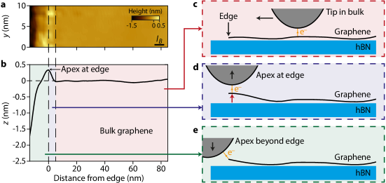
We show in Fig. S3a the topographic map obtained from a CITS toward the graphene armchair edge identified in Fig. S2. is the distance from the armchair edge, while is the lateral coordinate parallel to the edge. The topographic map features a clean and flat bulk graphene on a nm2 area next to the edge. When the tip is situated a few nanometers away from the edge, the map reveals inhomogeneous bright spots. Though one can first think about residues, the small height of these spots, around , rules out this hypothesis.
We rather attribute these large spots to the lifting of the edge of the graphene sheet, as illustrated in Fig. S3d. The attractive van der Waals force of the tip was shown [33] to lift locally a graphene sheet lying on a SiO2 substrate on a typical height of . Although we do not observe such lifting in Fig. S3a in bulk graphene (either because the deformation follows the tip such that we eventually observe an overall flat background, or because the deformation of the graphene sheet on hBN is more difficult, since the adhesion interactions between both materials are more important than between graphene and SiO2), we can assume that the graphene flake is more easily deformed at the edge by the force of the tip, and therefore the lifting is larger there than in the bulk.
The lifting of the edge is well visible in the height profile of Fig. S3b, obtained by averaging the topographic map along the direction (parallel to the edge). The profile features a flat region corresponding to bulk graphene (with variations of less than ), and a hump of height at the edge. After that, the tip quickly moves down by several nanometers until it meets the safety condition of the -controller, which stops the CITS. We attribute this lowering of the position to the fact that the tip apex has gone beyond the edge of graphene, but tunneling remains possible with some other higher atoms of the tip close to the apex, see Fig. S3d. This makes the measurement of a tunneling current possible even when the apex itself is lying on hBN, yet this current is highly unstable.
From this model we assume the position of the edge of graphene (i.e. the tip apex is atop the edge) is given by the maximum of the hump in the profile, and from this origin we compute the distance from the edge, which we use in the main text and the following figures.
IV Additional tunneling conductance maps at the edge
We show in this section two additional tunneling conductance maps acquired along the same armchair edge, but a few tens of nanometers away from the map shown in Fig. 2 of the main text. The back-gate voltage is fixed at V, corresponding to filling factor .
In Figs. S4 and S5, the panels (a) show the topographic map and the profile obtained by averaging the map on the lateral -dimension. Bulk graphene appears flat and clean, with a corrugation of at most on a distance of 100 and nm, respectively. When approaching the edge on the left, increases by around due to the tip-induced lifting of the graphene sheet edge. In Fig. S4 the CITS grid spectroscopy did not go beyond the edge: the edge position is rather roughly estimated using the STM image in Fig. 1d from the main text. The same goes for Fig. S5.
Panels (b) show the tunneling conductance toward the armchair edge as a function of the distance to the edge and the sample bias. The same qualitative observations as that of the main text can be made for the two edges: the Landau level peaks do not disperse when approaching the edges but vanish. The splitting of the LL0 is well visible and the gap stays open down to the edge where it even gets more pronounced.
Panel (c) in Fig. S4 shows the tunneling conductance as a function of the distance to the edge and the -direction parallel to the edge, at different bulk Landau level energies .
We now consider in more details the tunneling conductance map shown in Fig. S4b. We plot in Fig. S6a the evolution of the positions in energy of the visible LLN peaks and in Fig. S6b the variation of their height as a function of . The amplitude of the peaks decreases as we approach the edge until peaks merge into a V-shape background at the edge where they are no longer visible. In particular, LL4 vanishes at from the edge, LL3 at whereas LL2 and LL±1 disappear at . The amplitude of LL1 also vanishes way faster than the other LLN of higher index . In addition to the peak vanishing at the edge, we can also notice in Fig. S4b and S6a a weak dispersion toward higher energy of the LLN peaks close to the edge (on a length of around from the edge), see Ref. [28].
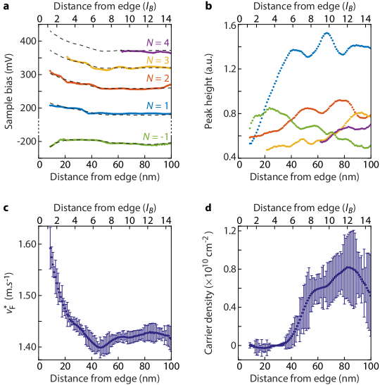
Furthermore, we can fit the positions of LLN≠0 at each (for every visible LL at this point) with respect to equation to extract an effective Fermi velocity and an estimate of the Dirac point position as a function of . These results are shown in Figs. S6c for and S6d for , which is converted into charge carrier density using . The bulk value m.s-1 is consistent with a renormalization of the Fermi velocity due to the enhancement of electron-electron interactions at charge neutrality [65, 47, 48], as characterized in a previous work [18] for the same sample AC04. Below the effective Fermi velocity starts to increase toward the armchair edge due to the dispersion of the LL peaks, reaching m.s-1 at from the edge. As for the carrier density, we obtain a residual value cm-2 in bulk graphene (in agreement with a back-gate voltage tuned at ). Below nm the density is seen to decrease and eventually vanishes at from the edge. A similar decrease of the density with respect to its bulk value has also been observed around from graphene edge on graphite [28]. Finally, we use the and parameters to plot in Fig. S6a the fitted energies of each LL (black dashed lines). We notice a good agreement with the experimental points, especially for the dispersing parts.
V Tunneling conductance gate maps at different distances from the edge
We show in this section additional tunneling conductance gate maps (Fig. S7) used to plot the evolution of the charge-neutrality point as a function of the distance from the edge in Fig. 3c of the main text. is estimated at the middle of the gap opening when LL0 pins the Fermi level at zero bias. This gap due to exchange interaction is indeed expected to be maximal at charge neutrality (i.e. half filling).
In each panel we indicate the opening of the gap by yellow dashed lines, observed as :
-
-
either as a typical gap opening between both LL such as in panel (i,j),
-
-
either as a kink toward negative energies in the LL peak around zero sample bias, when the LL is not visible, such as in panels (b-h),
-
-
either as a kink in the other LL peaks or charging peaks when not easily visible for LL0, such as in panel (a).
Note that the opening of the gap at zero sample bias also induces a shift in energy of other LL peaks (and also of charging peaks), which enables unambiguous identification of the charge-neutrality point. Still these shifts in energy do not occur strictly at constant gate voltage due to tip-induced gating, see for instance the red dashed line in Fig. S7c.