Probing itinerant carrier dynamics at the diamond surface using single nitrogen vacancy centers
Abstract
Color centers in diamond are widely explored for applications in quantum sensing, computing, and networking. Their optical, spin, and charge properties have been extensively studied, while their interactions with itinerant carriers are relatively unexplored. Here we show that NV centers situated within 10 nm of the diamond surface can be converted to the neutral charge state via hole capture. By measuring the hole capture rate, we extract the capture cross section, which is suppressed by proximity to the diamond surface. The distance dependence is consistent with a carrier diffusion model, indicating that the itinerant carrier lifetime can be long, even at the diamond surface. Measuring dynamics of near-surface NV centers offers a new tool for characterizing the diamond surface and investigating charge transport in diamond devices.
Color centers have been widely studied for their applications in quantum sensing, quantum networks, and quantum information processing Childress and Hanson (2013); Hong et al. (2013); Schirhagl et al. (2014). Nitrogen vacancy (NV) centers in diamond in particular are an attractive platform because they exhibit long spin coherence times at room temperature and they allow for off-resonant optical detection and initialization of spin states Childress and Hanson (2013); Bar-Gill et al. (2013). Charge state stability and control of NV centers is of particular interest for applications in nanoscale sensingStaudacher et al. (2013); Mamin et al. (2013), superresolution microscopyChen et al. (2015) and long-term data storageDhomkar et al. (2016). Recent experiments have focused on selectively preparing Kurtsiefer et al. (2000); Rondin et al. (2010); Cui and Hu (2013); Schreyvogel et al. (2015) and reading out Neumann et al. (2010); Robledo et al. (2011); Shields et al. (2015) particular charge states, as well as studying the impact of charge dynamics on optically detected magnetic resonance Yuan et al. (2020); Bluvstein, Zhang, and Jayich (2019). However, the interactions between itinerant carriers and color centers is less well explored, and can strongly impact the color center charge state, ionization dynamics, and spin readout. Such interactions could also be harnessed for new functionality such as electrically detected magnetic resonance, Hrubesch et al. (2017); Siyushev et al. (2019) and stabilizing non-equilibrium charge distributions Dhomkar et al. (2018); Zhang et al. (2022).
Recent work has focused on using itinerant carriers to manipulate color centers in the diamond bulk. For example, it was shown that the optically dark state of a silicon vacancy (SiV) center is SiV2- through charge state readout of NV centers and SiV centers combined with remote optical pumping Gardill et al. (2021). In another example, holes generated by one NV center were captured by another NV center, converting the latter NV center to the neutral charge state Lozovoi et al. (2021). Both studies examined NV centers far (>10 m) from the surface, at which distances surface effects are negligible.
Here we study charge dynamics of shallow NV centers <10 nm from the surface and their interaction with itinerant carriers. Shallow defects are essential for high sensitivity quantum sensing, and understanding the NV charge state and itinerant carrier dynamics near the surface is critical for developing shallow NV centers as a quantum platform. We demonstrate that the charge state of a shallow probe NV center (NVP) can be controlled by free carriers generated by excitation of another remote shallow source NV center (NVS) up to 7 m away (Fig. 1(a, b)). Specifically, the charge state of NVP converts from negative to neutral as a second 532 nm excitation laser is scanned over NVS (Fig. 1(c)). Continuous optical ionization and recombination of NVS generates a constant flow of holes and electrons in the valence and conduction bands, respectively. These itinerant carriers can diffuse and subsequently be captured by NVP. The net conversion to the neutral charge state implies that hole capture is much more efficient than electron capture, leading to a net change in the steady-state charge. This phenomenon has been observed in some previous works Gardill et al. (2021); Lozovoi et al. (2021).
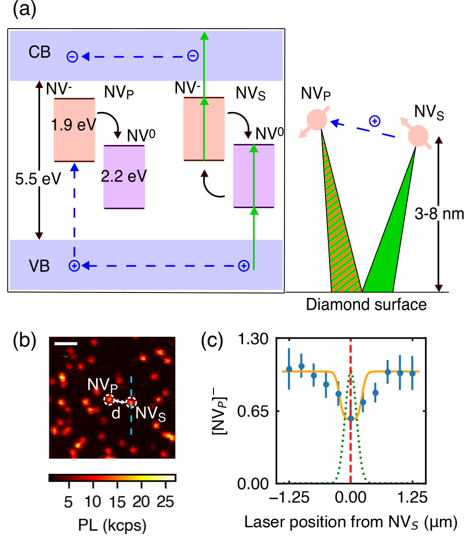
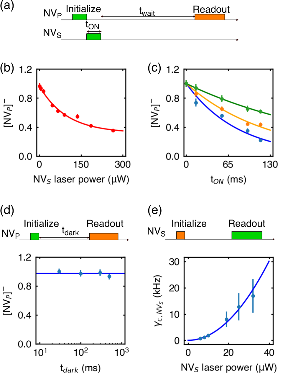
NV centers are individually interrogated using a dual channel, multicolor confocal microscope (see methods). In the experiment, two optically resolvable NV centers are chosen within the scanning field of view, NVP and NVS. One optical channel monitors the charge state of NVP after initialization into NV- with roughly 70% probability using a high power green pulse (94 W, 5 ms), followed by charge state readout with a low power orange pulse (2 W, 150 ms). In between these pulses, the second optical channel is used to pump NVS for a time tON with a green laser pulse of variable power, cycling its charge state between NV- and NV0 (Fig. 2(a)). This cycling generates free carriers that diffuse away and can be subsequently captured by nearby NV centers. The charge state population is measured by obtaining fluorescence with orange excitation since 591 nm is situated in between the zero phonon lines (ZPL) of NV- (637 nm) and NV0 (575 nm). A time window shorter than the decay time obtained from the fluorescence trace is defined, over which a histogram of photon counts is drawn. The area under the double Poisson shaped histogram is used to determine the charge state population of NVP (see Supplementary Material for details).
We interrogate the charge capture kinetics by measuring the charge state of NVP while varying the excitation power at NVS. As the excitation power increases, the population of the negative charge state ([NVP]-) decreases (Fig. 2(b)). Moreover, [NVP]- decays exponentially with the duration of the NVS excitation pulse, and the decay time constant decreases with increasing excitation power (Fig. 2(c)). Without any excitation at NVS, there is no change in [NVP]- over time (Fig. 2(d)). The net decay of [NVP]- during NVS illumination indicates that hole capture in the negative charge state dominates over electron capture in both the negative and neutral charge states.
We model the hole capture rate, as:
| (1) |
where is the hole density, is the capture coefficient, is the hole generation rate at NVS, is an effective hole diffusion length that arises from the free carrier lifetime, is the distance between NVS and NVP, is the hole capture cross-section at NVP, is the hole velocity, and is the dark ionization rate, which is constant. The factor of two in the numerator of equation (1) arises from a geometrical factor–we assume that carriers can reflect from the surface, and the NV centers are much closer to the surface than they are to each other. To calculate (Fig. 2(e)), we first fit the fluorescence of NVS under 532 nm illumination (after initialization with 591 nm laser) to an exponential fit to extract the total charge conversion rate, = + of NVS, where and are ionization and recombination rates respectivelyYuan et al. (2020) (see Supplementary Material for details). We measure the NV- population of several NV centers in our sample at steady state for several powers of 532 nm initialization. All of the measured NV centers show NV- population in the range of [55%, 70%], which along with is used to calculate , and subsequently . In steady state, since the time between subsequent holes is the total time it takes for a hole and an electron to be generated, we have .
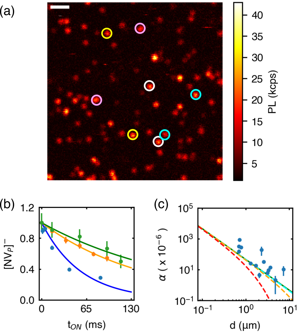
We measured 17 pairs of NV centers in total and observed hole capture in 14 of the pairs (Fig. 3(a)). The hole capture rate varies among pairs of NV centers, and is generally slower for NV pairs with larger spacing (Fig. 3(b)). This distance dependence could arise from the area scaling of carrier diffusion or from a finite carrier lifetime. By rearranging equation (1) we can define a parameter to investigate if the hole carrier lifetime is an important factor, where
| (2) |
We assume = 0 because the run time of the experiment (< 600 ms) is shorter than the dark lifetime of NVP (Fig. 2(c), see Supplementary Material for details). The calculated for each NV pair is plotted versus inter-NV distance in Fig. 3(c). The distance dependence is consistent with a 1/ scaling (see Supplementary Material for details). We therefore conclude that the effective ionization of NVP due to NVS is not limited by the diffusion length of holes.
From the fit in Fig. 3(c), we extract the capture cross-section, = 2.8910-4 0.5410-4 m2. The large value of likely arises from the Coulomb attraction between the negatively charged NV center and the hole, resulting in Rydberg-like states Zhang et al. (2020). We note that although the cross section is large, this value is an order of magnitude smaller than previously reported for deep NV centers Lozovoi et al. (2021). The surface-related suppression of hole capture could arise from finite hole lifetime due to surface traps or reduction in the effective cross section because of geometric overlap with the surface. We rule out the former reason based on the distance dependence shown in Fig. 3(c).
We have demonstrated generation and capture of free carriers between two shallow NV centers that are 10 m apart from one another. We have shown that the hole capture cross section is smaller than prior measurements of bulk NV centers, but that the observed carrier capture rate is not limited by the carrier lifetime. The hole diffusion length and hole capture cross section can be utilized as sensitive probes of charge transport in diamond devices. The technique demonstrated here can be easily extended to stabilize particular charge states of defects through photo-doping with distant donors, rather than bulk doping, as we have recently demonstrated for SiV0 centers Zhang et al. (2022). A natural next step would be to deploy photodoping to stabilize new color centers such as GeV0, SnV0 and PbV0.
METHODS
Diamond samples are prepared using the same process detailed in the previous workSangtawesin et al. (2019). Diamond substrates from Element Six (E6) are laser cut and scaife polished to a (100) face within a 3 degree specification. They are then reactive ion etched under Ar/Cl2 and then under O2. This etching damage is removed by a 1200∘C vacuum anneal. The resulting amorphous carbon layer is removed by refluxing a 1:1:1 mixture of perchloric, nitric, and sulfuric acids for at least two hours (triacid clean). The samples are then implanted with 15N at 3 keV at a dose of 0.5109 cm-2. Following ion implantation, samples are triacid cleaned and then vacuum annealed at 800∘C to form nitrogen-vacancy complexes. Following another triacid clean, the samples are then oxygen annealed at 460∘C to form a well-ordered oxygen-terminated surface.
To investigate the charge state modification, NV centers are interrogated using multicolor confocal microscope with two excitation pathways. These excitation pathways each pass through two galvanometers (model: Thorlabs GVS012) before being combined into the objective. Photons collected from the sample are counted through two avalanche photodiodes (model: Excelitas SPCM-AQRH-44-FC). This allows for simultaneous optical control and measurement of two distinct NV centers. One excitation path contains only 532 nm laser (laser on NVS in Fig. 2(a) pulse sequence) from a laser source (model: Coherent Sapphire 532-300 LP), and is used to cycle the charge state of NVS. The other excitation path (laser on NVP in Fig. 2(a) pulse sequence) includes light from a continuum source (model: NKT SuperK, repetition rate 78 MHz, pulse width 5 ps), bandpass-filtered at 591 nm, in addition to 532 nm light from another branch of the same green laser source mentioned before. This path is used to interrogate the charge state of NVP. This setup is similar to the setup used in previous workYuan et al. (2020), the primary difference being the path interrogating NVS.
Laser light sources are coupled into acousto-optic modulators, allowing for pulses with sub 100 ns rise and fall times. A Pulse Blaster (model: SpinCore ESR-PRO500 with a timing resolution of 2 ns) is used to control the acousto-optic modulators and the timing of readout.
The photon count rate depends sensitively on the charge state of the NV center. As a result, a histogram of photon counts per trial reveals two peaks corresponding to the two charge states. Fitting these peaks to a double Poisson distributions then reveals the charge state probability.
SUPPLEMENTARY MATERIAL
See the Supplementary Material for details about determination of NV- population, calculation of carrier generation rate, diagnosis of dark ionization rate, verification of long diffusion length, and hole capture rates for concerned NV centers.
Acknowledgements.
We would like to thank Carlos Meriles and Artur Lozovoi for helpful discussions. This work was primarily supported by the US Department of Energy, Office of Science, Office of Basic Energy Sciences, under Award No. DE-SC0018978. Diamond surface preparation was supported by the NSF under the CAREER program (grant DMR1752047). J.A. acknowledges the NSF Graduate Research Fellowship Program for support. J.R. acknowledges the Princeton Quantum Initiative Postdoctoral Fellowship for support.Author Declarations
Conflict of Interest
The authors have no conflicts to disclose.
Author Contributions
M.M., J.A., J.R., and N.P.d.L. conceptualized the project, designed experiments, analyzed the data, and wrote the manuscript. M.M. and J.A. carried out experiments, Z.Y. and J.R. helped optimize the experimental apparatus and charge state readout. All authors contributed to writing and editing the manuscript.
Data Availability
The data that support the findings of this study are available from the corresponding author upon reasonable request.
References
References
- Childress and Hanson (2013) L. Childress and R. Hanson, “Diamond nv centers for quantum computing and quantum networks,” MRS bulletin 38, 134–138 (2013).
- Hong et al. (2013) S. Hong, M. S. Grinolds, L. M. Pham, D. Le Sage, L. Luan, R. L. Walsworth, and A. Yacoby, “Nanoscale magnetometry with nv centers in diamond,” MRS bulletin 38, 155–161 (2013).
- Schirhagl et al. (2014) R. Schirhagl, K. Chang, M. Loretz, and C. L. Degen, “Nitrogen-vacancy centers in diamond: nanoscale sensors for physics and biology,” Annu. Rev. Phys. Chem 65, 83–105 (2014).
- Bar-Gill et al. (2013) N. Bar-Gill, L. M. Pham, A. Jarmola, D. Budker, and R. L. Walsworth, “Solid-state electronic spin coherence time approaching one second.” Nature communications 4(1), 1–6 (2013).
- Staudacher et al. (2013) T. Staudacher, F. Shi, S. Pezzagna, J. Meijer, J. Du, C. A. Meriles, F. Reinhard, and J. Wrachtrup, “Nuclear magnetic resonance spectroscopy on a (5-nanometer) 3 sample volume,” Science 339, 561–563 (2013).
- Mamin et al. (2013) H. Mamin, M. Kim, M. Sherwood, C. Rettner, K. Ohno, D. Awschalom, and D. Rugar, “Nanoscale nuclear magnetic resonance with a nitrogen-vacancy spin sensor,” Science 339, 557–560 (2013).
- Chen et al. (2015) X. Chen, C. Zou, Z. Gong, C. Dong, G. Guo, and F. Sun, “Subdiffraction optical manipulation of the charge state of nitrogen vacancy center in diamond,” Light: Science & Applications 4, e230–e230 (2015).
- Dhomkar et al. (2016) S. Dhomkar, J. Henshaw, H. Jayakumar, and C. A. Meriles, “Long-term data storage in diamond,” Science advances 2, e1600911 (2016).
- Kurtsiefer et al. (2000) C. Kurtsiefer, S. Mayer, P. Zarda, and H. Weinfurter, “Stable solid-state source of single photons,” Physical review letters 85, 290 (2000).
- Rondin et al. (2010) L. Rondin, G. Dantelle, A. Slablab, F. Grosshans, F. Treussart, P. Bergonzo, S. Perruchas, T. Gacoin, M. Chaigneau, H.-C. Chang, et al., “Surface-induced charge state conversion of nitrogen-vacancy defects in nanodiamonds,” Physical Review B 82, 115449 (2010).
- Cui and Hu (2013) S. Cui and E. L. Hu, “Increased negatively charged nitrogen-vacancy centers in fluorinated diamond,” Applied Physics Letters 103, 051603 (2013).
- Schreyvogel et al. (2015) C. Schreyvogel, V. Polyakov, R. Wunderlich, J. Meijer, and C. Nebel, “Active charge state control of single nv centres in diamond by in-plane al-schottky junctions,” Scientific reports 5, 1–12 (2015).
- Neumann et al. (2010) P. Neumann, J. Beck, M. Steiner, F. Rempp, H. Fedder, P. R. Hemmer, J. Wrachtrup, and F. Jelezko, “Single-shot readout of a single nuclear spin,” science 329, 542–544 (2010).
- Robledo et al. (2011) L. Robledo, L. Childress, H. Bernien, B. Hensen, P. F. Alkemade, and R. Hanson, “High-fidelity projective read-out of a solid-state spin quantum register,” Nature 477, 574–578 (2011).
- Shields et al. (2015) B. J. Shields, Q. P. Unterreithmeier, N. P. de Leon, H. Park, and M. D. Lukin, “Efficient readout of a single spin state in diamond via spin-to-charge conversion,” Physical review letters 114, 136402 (2015).
- Yuan et al. (2020) Z. Yuan, M. Fitzpatrick, L. V. Rodgers, S. Sangtawesin, S. Srinivasan, and N. P. de Leon, “Charge state dynamics and optically detected electron spin resonance contrast of shallow nitrogen-vacancy centers in diamond,” Physical Review Research 2, 033263 (2020).
- Bluvstein, Zhang, and Jayich (2019) D. Bluvstein, Z. Zhang, and A. C. B. Jayich, “Identifying and mitigating charge instabilities in shallow diamond nitrogen-vacancy centers,” Phys. Rev. Lett. 122, 076101 (2019).
- Hrubesch et al. (2017) F. M. Hrubesch, G. Braunbeck, M. Stutzmann, F. Reinhard, and M. S. Brandt, “Efficient electrical spin readout of nv- centers in diamond,” Physical review letters 118, 037601 (2017).
- Siyushev et al. (2019) P. Siyushev, M. Nesladek, E. Bourgeois, M. Gulka, J. Hruby, T. Yamamoto, M. Trupke, T. Teraji, J. Isoya, and F. Jelezko, “Photoelectrical imaging and coherent spin-state readout of single nitrogen-vacancy centers in diamond,” Science 363, 728–731 (2019).
- Dhomkar et al. (2018) S. Dhomkar, P. R. Zangara, J. Henshaw, and C. A. Meriles, “On-demand generation of neutral and negatively charged silicon-vacancy centers in diamond,” Physical review letters 120, 117401 (2018).
- Zhang et al. (2022) Z.-H. Zhang, A. M. Edmonds, N. Palmer, M. L. Markham, and N. P. de Leon, “Neutral silicon vacancy centers in diamond via photoactivated itinerant carriers,” arXiv preprint arXiv:2209.08710 (2022).
- Gardill et al. (2021) A. Gardill, I. Kemeny, M. C. Cambria, Y. Li, H. T. Dinani, A. Norambuena, J. R. Maze, V. Lordi, and S. Kolkowitz, “Probing charge dynamics in diamond with an individual color center,” Nano Letters 21, 6960–6966 (2021).
- Lozovoi et al. (2021) A. Lozovoi, H. Jayakumar, D. Daw, G. Vizkelethy, E. Bielejec, M. W. Doherty, J. Flick, and C. A. Meriles, “Optical activation and detection of charge transport between individual colour centres in diamond,” Nature Electronics 4, 717–724 (2021).
- Zhang et al. (2020) Z.-H. Zhang, P. Stevenson, G. Thiering, B. C. Rose, D. Huang, A. M. Edmonds, M. L. Markham, S. A. Lyon, A. Gali, and N. P. De Leon, “Optically detected magnetic resonance in neutral silicon vacancy centers in diamond via bound exciton states,” Physical review letters 125, 237402 (2020).
- Sangtawesin et al. (2019) S. Sangtawesin, B. L. Dwyer, S. Srinivasan, J. J. Allred, L. V. H. Rodgers, K. De Greve, A. Stacey, N. Dontschuk, K. M. O’Donnell, D. Hu, D. A. Evans, C. Jaye, D. A. Fischer, M. L. Markham, D. J. Twitchen, H. Park, M. D. Lukin, and N. P. de Leon, “Origins of diamond surface noise probed by correlating single-spin measurements with surface spectroscopy,” Phys. Rev. X 9, 031052 (2019).