Dynamics of van der Waals Charge Qubit in 2D Bilayers: Ab initio Quantum Transport and Qubit Measurement
Abstract
A van der Waals (vdW) charge qubit, electrostatically confined within two-dimensional (2D) vdW materials, is proposed as building block of future quantum computers. Its characteristics are systematically evaluated with respect to its two-level anti-crossing energy difference (). Bilayer graphene ( 0) and a vdW heterostructure ( 0) are used as representative examples. Their tunable electronic properties with an external electric field define the state of the charge qubit. By combining density functional theory and quantum transport calculations, we highlight the optimal qubit operation conditions based on charge stability and energy-level diagrams. Moreover, a single-electron transistor (SET) design based on trilayer vdW heterostructures capacitively coupled to the charge qubit is introduced as measurement setup with low decoherence and improved measurement properties. It is found that a greater than 20 meV results in a rapid mixing of the qubit states, which leads to a lower measurement quantity, i.e. contrast and conductance. With properly optimized designs, qubit architectures relying on 2D vdW structures could be integrated into an all-electronic quantum computing platform.
I Introduction
Emerging nanoelectronic devices are widely seen as key enablers of future quantum computers that will be able to solve intractable problems for classical machines. A wide range of qubit platforms have already been experimentally demonstrated, e.g. charge, spin, superconducting, and trapped-ion qubits [1, 2, 3, 4]. In all these approaches, a large number of physical qubits are required to realize one single logical qubit [5]. The ideal qubit structure should therefore be scalable and integrable with the existing CMOS technology to build a large-scale quantum computer.
Quantum dots (QD) offer a great platform to generate CMOS-compatible qubits based on the spin and/or electronic orbital degrees of freedom of electrons [6, 7, 8]. For example, silicon spin qubits show very long coherence times up to milliseconds at low temperature [2]. However, they are rather challenging to handle due to the rapid flip-flop of single electron spins. Charge qubits, on the other hand, can simplify the read-out of qubits thanks to well-developed technologies such as single-electron transistors (SET). Moreover, these qubits can be directly operated by electrodes up to gigahertz rates.

Two-dimensional (2D) materials represent a promising alternative to conventional semiconductors to host qubits owing to the wide tunability of their electronic properties and the manyfold quantum phenomena that emerge in the atomically thin limit such as massless Dirac fermions [9], anyons [10], or the quantum spin Hall effect [11]. In addition, the van der Waals (vdW) stacking of 2D materials provides versatility in growth, functionalization, and heterostructure integration, which facilitates the processing of complex systems. AB-stacked bilayer graphene (BLG), a vdW homojunction, is an excellent example: its band gap can be gradually modified by applying an external electric field [12, 13, 14, 15, 16, 17, 18]. Moreover, the electric field can modify the quantum superposition of wave functions localized in different layers, affecting both the conduction and valence bands of BLG. The same effect can be obtained in other vdW structures as well if the band edges of the individual 2D materials that constitute the stack get nearly aligned on an absolute energy scale [19]. Based on this observation, vdW structures are attractive to implement charge qubits capable of switching between two states with the help of a vertical electric field [20]. However, for vdW charge qubits to become a viable option, an all-electronic platform that can host multiple QDs should be available. The coupling between neighboring QDs should be tunable, while it should be possible to measure the qubit state with low decoherence.
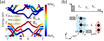
In this work, we propose a platform for vdW charge qubits that takes advantage of quantum superposition of the top and bottom charge states formed by vdW bilayers, as illustrated in Fig. 1(a), and we analyze its potential through ab initio device simulations. Differently from the conventional charge qubits that require two QDs, e.g. the left and right QDs, a single QD of bilayer acts as an individual qubit. As a promising candidate, we showcase the functionality of a BLG vdW charge qubit system. The role of two-level anti-crossing energies is analyzed for two exemplary vdW materials that illustrate the extreme cases of : BLG () and ZrS2-HfS2 ( eV). As a first step, density functional theory (DFT) and quantum transport calculations are combined to study the charge stability diagram and energy-level spectrum of multiple vdW charge qubits with tunable coupling, formed on an electrostatically confined BLG device. It should be pointed out that directly coupled read-out leads, as originally proposed in the paper of Lucatto et al. [20], can be prominent sources of decoherence due to the finite tunnel coupling of the reservoirs to the charge qubit. As a consequence, it might be experimentally difficult to measure the qubit state. To overcome this issue, we designed a novel measurement setup using triple-QD SETs based on a trilayer vdW heterostructure electrostatically coupled to our vdW charge qubits, as depicted in Fig. 1(b). Here, its influence will be simulated through the Lindblad master equation with the QuTiP package [21] using a phenomenological model including the important physics of decoherence. Our results highlight that 2D vdW structures can provide highly integrable all-electronic universal qubits. Moreover, our findings indicate that devices with 20 meV pose specific design challenges related to the material combination and geometrical parameters. Hence, a careful selection of the value is necessary to design properly working vdW charge qubits.
II vdW charge qubit manipulation
We first examine the effect of a vertical electric field on the selected 2D vdW bilayer materials, BLG and ZrS2-HfS2, and show that the electric-field externally applied to the bilayers can be used to control the wave function localized in the top or bottom layer to construct the qubit states. The BLG band structure without and with electric field is shown in Figs. 2(a) and 2(b), respectively. The detailed DFT simulation procedure that was used to compute those quantities can be found in Appendix A. The conduction band minimum (CBM) and valence band maximum (VBM) are chosen as the two-level qubit states ( and ) in the case of BLG, while the first and second lowest conduction bands of the ZrS2-HfS2 heterostructure play the same role. One importance for vdW bilayers to properly act as qubits is the existence of two bands lying quite close to each other and that can be easily inverted by applying a practical electric field.
In the BLG system without electric field , the and states are made of exactly equal contributions from each graphene layer due to the inversion symmetry of this material. A bandgap can be opened by applying a symmetry-breaking vertical . The vdW charge qubit states, and , are constructed by combining the wave functions localized in the top and bottom layers, and , respectively.
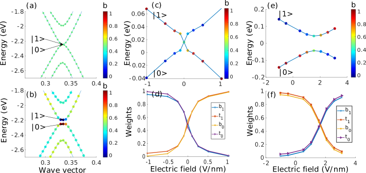
By applying a positive along the direction, as in Fig. 1(a), the bands of the bottom graphene layer are lowered in energy, which increases the character of , while becomes more localized in the top graphene layer. The opposite behavior happens with pointing along the direction. The contribution of each layer to the Bloch wave function of and strongly depends on the vertical electric field. An electron wave function can be written as the superposition of the wave functions and for a given
| (1) |
where and are complex coefficients depending on . Due to the vdW gap between the two layers, the and states have a relatively small overlap and form a quasi-orthogonal basis. The and coefficients satisfy the normalization condition .
Figure 2(c) shows the energy level of the and states and the contribution to them as a function of . In Fig. 2(d) the and weights of the and states are plotted, highlighting a complementary relation between them. Here, we note that by tuning we can readily address any coherent superposition of the basic quantum states and . The state can be equivalently described by a Bloch vector in the standard Bloch sphere representation, where the coefficients are given by a polar and azimuthal angle such that and . Moreover, under a reasonably strong positive/negative electric field, the and states can be localized in either the top or bottom layer, thus enabling the “must-have” qubit initialization process.

A similar behavior is observed for the first and second lowest conduction band states of ZrS2-HfS2, as depicted in Fig. 2(e) and (f). Due to the energy offset in the natural band alignment of the vdW heterostructure, a non-zero is required to reach the crossing point where the layer contributions are equal. At this point, a so-called anti-crossing energy can be introduced. The latter is then a material parameter and determined as the difference between the energies of the and eigenstates [1]. Table I summaries the values of for the considered vdW structures. For BLG, we note that eV was observed in previous experiments [14, 22, 23] due to the presence of symmetry-breaking factors even in the absence of an electric field, for example spin-orbit coupling, surrounding substrate atoms, or local strain.
By comparing our results to the ZrSe2-SnSe2 vdW heterostructure investigated in the original paper of Lucatto et al. [20], we notice that the Bloch vector of the BLG and ZrS2-HfS2 systems covers a larger interval for electric fields within 3 V/nm. For BLG, the full range of can be achieved with a small electric field of less than 1 V/nm, thus making BLG the most technologically appealing candidate.
A quantum control technique over the angle (i.e. relative phase of the wave functions) applicable to the vdW charge qubits has been proposed in Ref. 24. It relies on the Landau-Zener-Stückelberg (LZS) interference when the system non-adiabatically sweeps through the intersection point. Based on this technique, general rotations in the Bloch sphere and universal single qubit operations have already been experimentally demonstrated for Si and GaAs DQD charge qubits [1, 24].
III Quantum transport simulations
To create a clear two-level system with a and state, the QDs in the vdW bilayers must be formed electrically through gate electrodes that induce a local confinement, as illustrated in Fig. 3(a). In the proposed device setup, a bottom gate uniformly acts on the BLG encapsulated within two hBN dielectric layers to electrostatically control the Fermi level. A transport channel can be defined through the BLG. Separated by an oxide, three top gates labeled L, M, and R are placed. By applying different potentials to the bottom and top gates, the vertical electric field acting on the BLG can be precisely controlled. In addition, the potential landscape can be modified by tuning the top L, M, and R gates. The simulated device structure measures 260 nm along the transport direction, possesses zigzag edges, and is made of 42400 atoms in total. The three top gates are 10 nm long and separated by 50 nm. Charge transport is solved with a quantum transport simulator [25] based on the ab initio Non-equilibrium Green’s function (NEGF) formalism, as described in Appendix A. In this study, the potential profiles are approximated as Gaussian functions that are plotted in the bottom inset of Fig. 3(a), Poisson’s equation being not self-consistently solved due to the large computational burden associated with the consideration of thousands of gate voltage configurations.
Figure 3(b) shows that by applying V/nm and by properly adjusting the applied top gate voltages both electron and hole QDs can be generated in BLG, without spurious bandgap states and with a strong localization of the and states in the top and bottom graphene layer. The projected local density-of-states (LDOS) confirm that the qubit state defined in Fig. 2 is not altered by the confinement potential. By applying an appropriate bias to the top M gate (or plunger gate), a gradual transition from two QDs hosting electrons or holes to a single larger QD can be achieved, thus providing a way to tune the interdot tunnel coupling. This transition occurs between regime I and II in Fig. 3(c). The charge stability is demonstrated by the distinct resonances in the conductance map as a function of the gate voltages applied to the L and R electrodes, , setting . creates two potential barriers that confine an electron dot (ED) in the middle and that tune its energy levels. Each time an energy level crosses the energy window defined by the Fermi energies of the source and drain contacts, a resonance peak can be seen in the conductance map (see Fig. 3(d)). In addition to creating n and p-type QDs in the central region, the electrostatic potential can also be shaped to form ambipolar QDs through the application of large enough L and R gate voltages, as highlighted by regime III in Fig. 3(c). The L/R gates closely control the energy levels in the hole dot (HDL/HDR) underneath it. Whenever the energy levels of the ED and HDL/HDR cross the energy window of interest, a crossing of two lines of maximum conductance can be observed in Fig. 3(d). We note that the observed high LDOS on the QD boundaries, which originated from the coupling to the continuum of states in the left and right contacts due to the NEGF open boundary condition, is expected to be reduced in a fully self-consistent Schrödinger-Poisson solution. However, we do not expect this to alter qualitatively our result because the conductance is limited by the electron states inside the quantum dot rather than in the boundaries.

In order to investigate the system scalability towards a highly integrable qubit platform, we also show the posibility of creating multiple qubits within one BLG device in Fig. 4. Since the electron and hole dots possess well-separated LDOS and charge densities localized in the top and bottom layers, they can be exploited for hosting and qubit states. It is worth noting that between the QDs, the Fermi energy lies inside the band gap, which leads to a finite region of zero charge density and a tunneling barrier. Figure 4(a) shows an n-p double-QD, while Fig. 4(b) presents a p-n-p triple-QD formed in the channel. A chain of QDs of and can be constructed via top gates, thus promising easily scalable multi-qubit systems [8]. Contrary to the traditional charge qubits where two QDs are required to form a single charge qubit [1, 26], a single vdW-bilayer QD is sufficient to form one qubit because the wave function in each dot is a quantum superposition of and . Moreover, a single global bottom gate electrode reduces the number of gate electrodes, which greatly simplifies the geometrical complexity and increases the integration density of qubits. Coupling remote charge qubits has been experimentally demonstrated for graphene [27, 28] using microwave resonators, offering the possibility to entangle more-than-nearest-neighbor QDs. While the previous experiments show a viable path to implement a multi-qubit coupling scheme for the vdW-bilayer QDs, this remains a challenging task that will need detailed investigations in the future. They go far beyond the scope of our present work.
IV Time-dependent qubit measurement
After demonstrating the qubit operation conditions and obtaining charge stability for multiple QDs, the procedure to read out the qubit state is now discussed. For time-dependent simulations, the qubit is modeled by a two-level Hamiltonian constructed from the DFT bandstructure of 2D bilayers under different vertical electric fields
| (2) |
where and are the on-site energies of the top and bottom layer that depend linearly on , and is the anti-crossing energy. These values are obtained by fitting the VBM and CBM energy levels for varying (see Fig. 2) to the eigenvalues of the quadratic Hamiltonian.
A SET formed by a linear array of three QDs capacitively coupled to the qubit is chosen for the measurement, as suggested in Ref. [29] and shown in Fig. 5(b). Such a configuration has an enhanced readout sensitivity as compared to the more common single QD SET. The designed SET is described by the following Hamiltonian operator,
| (3) |
where , , and denote the single-electron states when the electron is located in QDL, QDR, and QDC, respectively, and , , and for the on-site energies; and indicate the tunneling probabilities between the QDs; , and are the two-electron states, while represents the Coulomb interaction between dots and . The electron density in the QD is assumed as a point charge. In this case the energies of the electrostatic interaction have the following values , where is the distance between the centers of the QDs and , m is the Bohr radius, Ry = 13.6 eV is the Rydberg energy. This approximation works well for small-sized charge dots as the ones considered in this work [29]. The SET is only coupled to the qubit the Coulomb interactions without any direct tunneling,
| (4) |
The time evolution of the density matrix operator corresponding to the qubit-SET system was simulated by solving the Lindblad equation [29, 30]. More details are given in Appendix B.
The optimal condition for the aforementioned triple-QD SET requires first that the energetic detunings between the external (QDL, QDR) and the central (QDC) dots, , are equivalent. Second, the electrostatic couplings between the SET QDs and the qubit should be symmetric (asymmetric) for the electron in the top (bottom) layer, respectively. More explicitly, and . We therefore propose a vdW heterostructure made of three 2D materials (MoS2-WSe2-MoS2) as SET design, as illustrated in Fig. 1(b).
The projected bandstructure in Fig. 5(a) reveals that the CBM and VBM are located within one of the 2D layers. The degenerate CBM of the top and bottom MoS2 layers define the energies of the external QDs L and R, and the VBM of WSe2 realizes the central QD C. The direct bandgap at K in the Brillouin Zone corresponds to the symmetric detuning . The vertical alignment of the top qubit layer with WSe2 guarantees that the presence of an electron in this layer causes a symmetric renormalization of the energies in the SET. In contrast, an electron in the qubit bottom layer creates an imbalance of detunings and causes the current to cease. The triple-QD in the vdW heterostructure is formed electrically by a top gate electrode that induces a local confinement. To asses the impact of electron-phonon and electron-electron interactions on the measurement sensitivity of the coupled qubit and SET systems, we included the relaxation and dephasing rates and , accounting for those scattering processes, respectively. The corresponding collapse operator in the Lindblad equation is constructed as
| (5) |
where .
The qubit is initialized by the application of an external electric field into one of the two states or . The system then evolves until it reaches a steady state at time where is the escaping rate of the electrons to the drain (see Fig. 5(b)). The output current is proportional to the population in the SET state . In what follows, we set = = 0.12 THz in agreement with experimental studies [1]. To assess the measurement capabilities of the proposed SET we record its contrast and conductance during the qubit dynamics. Here, the contrast determines how well both qubit states can be distinguished. It is defined as
| (6) |
where and denote the output current when measuring a qubit in the and states, respectively. The differential conductance quantifying the SET current changes caused by variations of the qubit states is defined as [29]
| (7) |
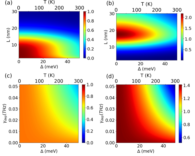
The resulting contrast and differential conductance are plotted in Fig. 6 as a function of the qubit anti-crossing energy and distance between the qubit and SET with a characteristic time of , including the aforementioned dissipative processes ( THz based on low-temperature transport measurement [31], while to account for the fact that dephasing happens faster than relaxation). The bottom left corner of Fig. 6(a) shows the limiting range of (up to 13 nm) and (up to 25 meV) to obtain high contrasts. Figure 6(b) also reports that decreases as a function of , but in a limited range of values between and nm. Combining both sub-plots, it clearly appears that the optimal conditions for qubit measurement are =12.5 nm and between 0 and 25 meV. The maximum value is higher than the experimental value reported in Ref. [32] using a different SET setup. A widely accepted idea is that a large is desired between the qubit states, in order to make them energetically distinguishable from each other. A necessary, but insufficient condition is that must be larger than two times the thermal energy () to suppress thermalization effects [33]. Therefore, a smaller value necessarily entails a lower operation temperature of the qubit, as indicated by the upper abscissa axis in Fig 6. Here, we show that a normally functional qubit also imposes an upper-limit on , thus reducing the qubit design space.
To examine the intrinsic feasibility of vdW charge qubits, we study and as a function of the dephasing rate and anti-crossing energy in Fig. 6(c) and (d). The distance between the SET and qubit is fixed to nm to ensure that both measurement quantities have high resolutions. It can be seen that the dephasing rate has a small impact on the degradation of and as long as remains below 20 meV. However, when exceeds 20 meV, and start to significantly decrease. This parameter region should therefore be avoided for the qubit design. This means that the anti-crossing energy is an intrinsically limiting factor, which suggests that the charge qubit should be defined with meV and the operating temperature lower than 120 K.
| BLG | ZrS2 (T) HfS2 (B) | |
|---|---|---|
| Contrast [%] | 71 | 26 |
| [S] | 102 | 35.7 |
| [meV] | 0.02 | 174 |
| [V/nm] | 0 | 1.6 |
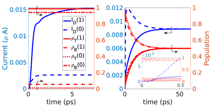
A typical time evolution of the drain current in this SET and the corresponding charge population in the qubit () and () states are presented in Fig. 7 for BLG and for ZrS2-HfS2. The BLG exhibits a much higher contrast of saturation current and almost no mixing. For ZrS2-HfS2, the strong results in a fast qubit state mixing and consequently requires very rapid measurements within the picosecond time scale. By reducing the strength of , for example by inserting an BN monolayer between the vdW bilayers, the qubit measurement quality can be recovered. These results underline the fact that high contrast qubit measurements are intrinsically not possible if the charge qubit is characterized by a large . Table I summaries the calculated qubit measurement results.
V Conclusion and Discussion
In this work, we proposed a vdW charge qubit architecture based on 2D vdW materials. Our results indicate that the qubit states can be readily controlled by external electric fields. The two-level anti-crossing energy, which is related to the vdW interlayer coupling strength, can significantly vary between different material systems. Our quantum transport simulations suggest that quantum dots can be confined by electrically gating the vdW bilayer and that the coupling between neighboring quantum dots can be tuned by the gate potential. Furthermore, we also proposed a single-electron transistor (SET) design based on a trilayer vdW heterostructure and capacitively coupled to the quantum dot to measure the charge qubit state. Our time evolution simulations of the coupled qubit and SET systems reveal that the measurement sensitivity and contrast are affected by the intrinsic anti-crossing energy and by the dephasing processes in the vdW heterostructure. Our study identifies the optimal design parameter space to simultaneously achieve a low decoherence of the qubit states and enhanced measurement contrast and conductance.
In conclusion, our theory explains that upon the SET measurement the vdW-heterostructure qubit states rapidly degrade due to the large coupling intrinsically induced by anti-crossing energies higher than 20 meV. This phenomenon was not captured by previous theoretical studies. Amoung the systems we studied, bilayer graphene is the one maintaining the highest contrast between qubit states. Our findings show that 2D vdW structures can provide highly integrable all-electronic universal qubits. Our design of the coupled vdW qubit and SET system allows for an enhanced sensitivity of the charge qubit, thus paving the way for a scalable and CMOS-compatible quantum computing platform.
Appendix A Ab initio quantum transport simulation
Following Ref. [20], a charge qubit can be defined in 2D bilayer materials through the superposition of a top () and bottom () orbital state, whose properties depend on a vertically applied electric field (). Since each local orbital occupies a different electrically-induced energy state, two distinct energy levels with different weights ( and ) can be obtained (Fig. 1(a)). They are used as building blocks for the Bloch sphere and its and states, which form the two-level quantum system shown in Fig. 1(b). The latter is simulated at the ab initio level.
Through the QUANTUM ESPRESSO DFT package [34], the electronic structure of 2D bilayer materials is first obtained. The generalized gradient approximation of Perdew, Burke, and Ernzerhof (PBE) [35] is used as exchange and correlation functional, while the vdW interactions are taken into account with the DFT-D2 scheme of Grimme [36]. The plane-wave DFT Hamiltonian is then converted into a maximally-localised Wannier function (MLWF) basis with the Wannier90 code [37]. These results are scaled up [38] to construct the real-space device Hamiltonian and to perform realistic qubit device simulations based on the Non-equilibrium Green’s Function (NEGF) formalism. The following equation is solved for the retarded Green’s function ,
| (8) |
where is the electron energy, the identity matrix, the Wannier Hamiltonian matrix of the 2D bilayer graphene in the MLWF basis, and the retarded boundary self-energy accounting for the source and drain semi-infinite contacts. The observables of the system can be obtained from the retarded Green’s function . The periodic boundary condition is imposed along the direction as shown in Fig. 3(a). By including an electrostatically-induced confinement potential into , a wide range of QD systems can be realized and their operation verified by inspecting the local density-of-states (LDOS). The electrical current of the device is calculated with the Landauer-Büttiker formula from the transmission probability between two contacts [39, 40]
| (9) |
with the elementary charge . The two contacts are characterized by their Fermi distribution function and Fermi levels and , whose difference depends on the applied source-to-drain voltage . The conductance is calculated as .
Appendix B Evaluation of time-dependent Lindblad equation for qubit readout
The dynamics of the charge qubits is simulated with the QuTiP [21] package, which solves the Lindblad equation [29],
| (10) |
where the qubit Hamiltonian () is a two-level quantum system constructed from the electronic structure of a 2D bilayer material, while a three-level QD is used to represent the SET Hamiltonian (). The qubit and SET parts are only electrostatically coupled through the electron-electron Coulomb interaction , assuming no tunneling between them. The dissipative processes including relaxation and dephasing are described by the collapse operators in Eq. (5). The meaning and definition of each operator are given in Section IV. An arbitrary state as in Eq. (1) is evolved by integrating the set of ordinary differential equations that define Eq. (10). The expectation value of the populations in the SET are recorded at each time step by means of the operators , , and . The output at the last time step is used in Eqs. (6) and (7) to asses the contrast and conductance of the proposed SET.
Acknowledgements.
This work was supported by the NCCR MARVEL and the NCCR SPIN of the Swiss National Science Foundation (SNSF), by SNSF under Grant No. 175479 (ABIME), by the Marie Skłodowska-Curie Grant No. 885893, and by a grant from the Swiss National Supercomputing Centre (CSCS) under Project s1119.References
- Gorman et al. [2005] J. Gorman, D. G. Hasko, and D. A. Williams, Phys. Rev. Lett. 95, 090502 (2005).
- Maurand et al. [2016] R. Maurand, X. Jehl, D. Kotekar-Patil, A. Corna, H. Bohuslavskyi, R. Laviéville, L. Hutin, S. Barraud, M. Vinet, M. Sanquer, and S. De Franceschi, Nat. Commun. 7, 13575 (2016).
- Gambetta et al. [2017] J. M. Gambetta, J. M. Chow, and M. Steffen, Npj Quantum Inf. 3, 2 (2017).
- Bruzewicz et al. [2019] C. D. Bruzewicz, J. Chiaverini, R. McConnell, and J. M. Sage, Appl. Phys. Rev. 6, 021314 (2019).
- Van Meter and Horsman [2013] R. Van Meter and C. Horsman, Commun. ACM 56, 84–93 (2013).
- Eich et al. [2018] M. Eich, R. Pisoni, A. Pally, H. Overweg, A. Kurzmann, Y. Lee, P. Rickhaus, K. Watanabe, T. Taniguchi, K. Ensslin, and T. Ihn, Nano Letters 18, 5042 (2018), publisher: American Chemical Society.
- Kurzmann et al. [2019] A. Kurzmann, H. Overweg, M. Eich, A. Pally, P. Rickhaus, R. Pisoni, Y. Lee, K. Watanabe, T. Taniguchi, T. Ihn, and K. Ensslin, Nano Letters 19, 5216 (2019), publisher: American Chemical Society.
- Banszerus et al. [2020] L. Banszerus, S. Möller, E. Icking, K. Watanabe, T. Taniguchi, C. Volk, and C. Stampfer, Nano Lett. 20, 2005 (2020).
- Novoselov et al. [2005] K. S. Novoselov, A. K. Geim, S. V. Morozov, D. Jiang, M. I. Katsnelson, I. V. Grigorieva, S. V. Dubonos, and A. A. Firsov, Nature 438, 197 (2005).
- Nayak et al. [2008] C. Nayak, S. H. Simon, A. Stern, M. Freedman, and S. Das Sarma, Rev. Mod. Phys. 80, 1083 (2008).
- Xiaofeng et al. [2014] Q. Xiaofeng, L. Junwei, F. Liang, and L. Ju, Science 346, 1344 (2014).
- McCann and Fal’ko [2006] E. McCann and V. I. Fal’ko, Phys. Rev. Lett. 96, 086805 (2006).
- McCann et al. [2007] E. McCann, D. S. Abergel, and V. I. Fal’ko, Solid State Communications 143, 110 (2007), exploring graphene.
- Aoki and Amawashi [2007] M. Aoki and H. Amawashi, Solid State Communications 142, 123 (2007).
- Castro et al. [2007] E. V. Castro, K. S. Novoselov, S. V. Morozov, N. M. R. Peres, J. M. B. L. dos Santos, J. Nilsson, F. Guinea, A. K. Geim, and A. H. C. Neto, Phys. Rev. Lett. 99, 216802 (2007).
- Oostinga et al. [2008] J. B. Oostinga, H. B. Heersche, X. Liu, A. F. Morpurgo, and L. M. K. Vandersypen, Nature Materials 7, 151 (2008).
- Mak et al. [2009] K. F. Mak, C. H. Lui, J. Shan, and T. F. Heinz, Phys. Rev. Lett. 102, 256405 (2009).
- Kumar and Guo [2011] S. B. Kumar and J. Guo, Appl. Phys. Lett. 98, 222101 (2011).
- Koda et al. [2018] D. S. Koda, F. Bechstedt, M. Marques, and L. K. Teles, Phys. Rev. B 97, 165402 (2018).
- Lucatto et al. [2019] B. Lucatto, D. S. Koda, F. Bechstedt, M. Marques, and L. K. Teles, Phys. Rev. B 100, 121406 (2019).
- Johansson et al. [2012] J. R. Johansson, P. D. Nation, and F. Nori, Comput. Phys. Commun. 183, 1760 (2012).
- Konschuh et al. [2012] S. Konschuh, M. Gmitra, D. Kochan, and J. Fabian, Phys. Rev. B 85, 115423 (2012).
- Banszerus et al. [2021] L. Banszerus, S. Möller, C. Steiner, E. Icking, S. Trellenkamp, F. Lentz, K. Watanabe, T. Taniguchi, C. Volk, and C. Stampfer, Nature Communications 12, 5250 (2021).
- Cao et al. [2013] G. Cao, H.-O. Li, T. Tu, L. Wang, C. Zhou, M. Xiao, G.-C. Guo, H.-W. Jiang, and G.-P. Guo, Nat. Commun. 4, 1401 (2013).
- Luisier [2014] M. Luisier, Chem. Soc. Rev. 43, 4357 (2014).
- Kim et al. [2015] D. Kim, D. R. Ward, C. B. Simmons, J. K. Gamble, R. Blume-Kohout, E. Nielsen, D. E. Savage, M. G. Lagally, M. Friesen, S. N. Coppersmith, and M. A. Eriksson, Nat. Nanotechnol. 10, 243 (2015).
- Deng et al. [2015a] G.-W. Deng, D. Wei, S.-X. Li, J. R. Johansson, W.-C. Kong, H.-O. Li, G. Cao, M. Xiao, G.-C. Guo, F. Nori, H.-W. Jiang, and G.-P. Guo, Nano Lett. 15, 6620 (2015a).
- Deng et al. [2015b] G.-W. Deng, D. Wei, J. R. Johansson, M.-L. Zhang, S.-X. Li, H.-O. Li, G. Cao, M. Xiao, T. Tu, G.-C. Guo, H.-W. Jiang, F. Nori, and G.-P. Guo, Phys. Rev. Lett. 115, 126804 (2015b).
- Tsukanov [2019] A. V. Tsukanov, Phys. Rev. A 100, 062305 (2019).
- Manzano [2020] D. Manzano, AIP Advances 10, 025106 (2020).
- Engels et al. [2014] S. Engels, B. Terrés, A. Epping, T. Khodkov, K. Watanabe, T. Taniguchi, B. Beschoten, and C. Stampfer, Phys. Rev. Lett. 113, 126801 (2014).
- Barthel et al. [2010] C. Barthel, M. Kjærgaard, J. Medford, M. Stopa, C. M. Marcus, M. P. Hanson, and A. C. Gossard, Phys. Rev. B 81, 161308 (2010).
- Makhlin et al. [2001] Y. Makhlin, G. Schön, and A. Shnirman, Rev. Mod. Phys. 73, 357 (2001).
- Giannozzi et al. [2017] P. Giannozzi et al., J. Phys.: Condens. Matter 29, 465901 (2017).
- Perdew et al. [1996] J. P. Perdew, K. Burke, and M. Ernzerhof, Phys. Rev. Lett. 77, 3865 (1996).
- Grimme [2006] S. Grimme, Journal of computational chemistry 27, 1787 (2006).
- Pizzi et al. [2020] G. Pizzi, V. Vitale, R. Arita, S. Blügel, F. Freimuth, G. Géranton, M. Gibertini, D. Gresch, C. Johnson, T. Koretsune, J. Ibañez-Azpiroz, H. Lee, J.-M. Lihm, D. Marchand, A. Marrazzo, Y. Mokrousov, J. I. Mustafa, Y. Nohara, Y. Nomura, L. Paulatto, S. Poncé, T. Ponweiser, J. Qiao, F. Thöle, S. S. Tsirkin, M. Wierzbowska, N. Marzari, D. Vanderbilt, I. Souza, A. A. Mostofi, and J. R. Yates, Journal of Physics: Condensed Matter 32, 165902 (2020).
- Szabó et al. [2019] A. Szabó, A. Jain, M. Parzefall, L. Novotny, and M. Luisier, Nano Letters 19, 3641 (2019), pMID: 31079463.
- Landauer [1988] R. Landauer, IBM Journal of Research and Development 32, 306 (1988).
- Büttiker [1990] M. Büttiker, Phys. Rev. Lett. 65, 2901 (1990).