Thermally-generated spin current in the topological insulator Bi2Se3
Abstract
We complete measurements of interconversions among the full triad of thermal gradients, charge currents, and spin currents in the topological insulator Bi2Se3 by quantifying the efficiency with which thermal gradients can generate transverse spin currents. We accomplish this by comparing the spin Nernst magneto-thermopower to the spin Hall magnesistance for bilayers of Bi2Se3/CoFeB. We find that Bi2Se3 does generate substantial thermally-driven spin currents. A lower bound for the ratio of spin current to thermal gradient is = (4.9 0.9) 106 () A m-2 / K m-1, and a lower bound for the magnitude of the spin Nernst ratio is 0.61 0.11. The spin Nernst ratio for Bi2Se3 is the largest among all materials measured to date, 2-3 times larger compared to previous measurements for the heavy metals Pt and W.
I Introduction
Topological insulators (TIs) provide the most-efficient known transduction between charge current density and spin current density (i.e., the spin Hall effect) [1, 2, 3, 4, 5], thereby producing spin-orbit torques capable of driving magnetization switching in magnetic memory structures [6, 7, 8]. In addition, TIs can also very efficiently transduce thermal gradients to electric field via the Seebeck effect [9, 10, 11], with potential for thermoelectric applications. Here, for the first time we measure the efficiency of transduction for all three legs of the triad between thermal gradients, charge currents, and spin currents for a topological insulator/magnet bilayer (see Fig. 1(b)). In particular, we provide the first measurement of the efficiency by which a thin film of the topological insulator Bi2Se3 can transduce a thermal gradient to spin current. Understanding thermally-generated spin currents in topological insulators is important for characterizing the effect of Joule heating on measurements of current-induced spin-orbit torques [12]. If the thermal spin currents are sufficiently strong, they could in principle be put to use in generating useful torques [13, 14]. We find that the magnitude of the spin Nernst ratio of Bi2Se3 is larger by a factor of 2-3 compared to previous reports for the heavy metals Pt [15, 16, 17, 18] and W [19, 16, 18].
II Background
We measure thermally-generated spin currents using the same physics by which electrically-generated spin currents give rise to the spin Hall magnetoresistance (SMR) effect. In the electrically-generated case, an electric field applied in the plane of a spin-source/ferromagnet bilayer gives rise to a vertically-flowing spin current density via the spin Hall effect, with an efficiency characterized by the spin Hall ratio, [20]: where is the reduced Planck constant, is the magnitude of the electron charge, and is the electrical resistivity of the spin-source material. The degree of reflection of this spin current at the magnetic interface depends on the orientation of the magnetization in the magnetic layer. The reflected spin current produces a voltage signal by the inverse spin Hall effect, causing the resistance of the bilayer to depend on the magnetization angle [21, 22, 23]: Here is the component of the magnetization unit vector that is in-plane and perpendicular to the electric field. This resistance change corresponds to a voltage signal amplitude:
| (1) |
with the total current through the bilayer, the total resistance of the bilayer, and the sample length. Our analysis will assume that a thermally-generated spin current produces the same voltage signal as an electrically-generated spin current (i.e., that Eq. 1 holds for both cases with the same experimentally-measured value of ).
An in-plane thermal gradient can similarly give rise to a vertically-flowing spin current in a spin-source layer via the spin Nernst effect [15, 18]. Upon reflection of this spin current from a magnetic interface and then the action of the inverse spin Hall effect, this results in a voltage signal parallel to the thermal gradient that depends on the magnetization angle, in direct analogy to the spin Hall magnetoresistance. For experiments measured with an open-circuit electrical geometry (i.e., no net longitudinal charge flow in the bilayer) we will define the efficiency of spin current generation by the spin Nernst effect in terms of a spin Nernst parameter
| (2) |
Here is the Seebeck coefficient of the spin-source layer and is the in-plane thermal gradient. The thermally-generated voltage takes the form [15, 19, 16]
| (3) |
where is the coefficient of the spin Nernst magneto-thermopower, is a magnetization-independent offset arising from the spin Nernst effect and inverse spin Hall effect, and and denotes the total effective Seebeck coefficient of the bilayer given by This approximation holds when the spin-source layer is a topological insulator such as Bi2Se3 for which the Seebeck coeeficient is much larger than for the ferromagnetic layer (), and we define a current shunting ratio where is the resistivity of the ferromagnet and and are the thicknesses of the two layers. As long as thermally-generated and electrically-generated spin currents are transduced to voltage the same way, we can combine Eqs. 1-3 to obtain
| (4) |
| (5) |
These are the two equations we will use to evaluate the thermally-generated spin current and the spin-Nernst ratio .
For an open-circuit measurement, will have contributions from both spin-current generated directly by a thermal gradient and spin current generated by an electric field that is also present due to the Seebeck effect. It is therefore also of interest to separate these effects and define a spin current that would be generated by a thermal gradient alone, in the absence of any electric field, i.e., to define a “bare” spin Nernst ratio such that
| (6) | ||||
| (7) |
Therefore, we can calculate
| (8) |
In our experimental geometry, a small vertical thermal gradient can also be present when we apply an in-plane thermal gradient. This will produce additional background signals due to the ordinary Nernst effect (ONE), the spin Seebeck effect (SSE) + inverse spin Hall effect, and the anomalous Nernst effect (ANE):
| (9) |
These signals will be distinguished from the voltages arising from an in-plane thermal gradient based on the different dependences on the magnetization orientation .
III Results
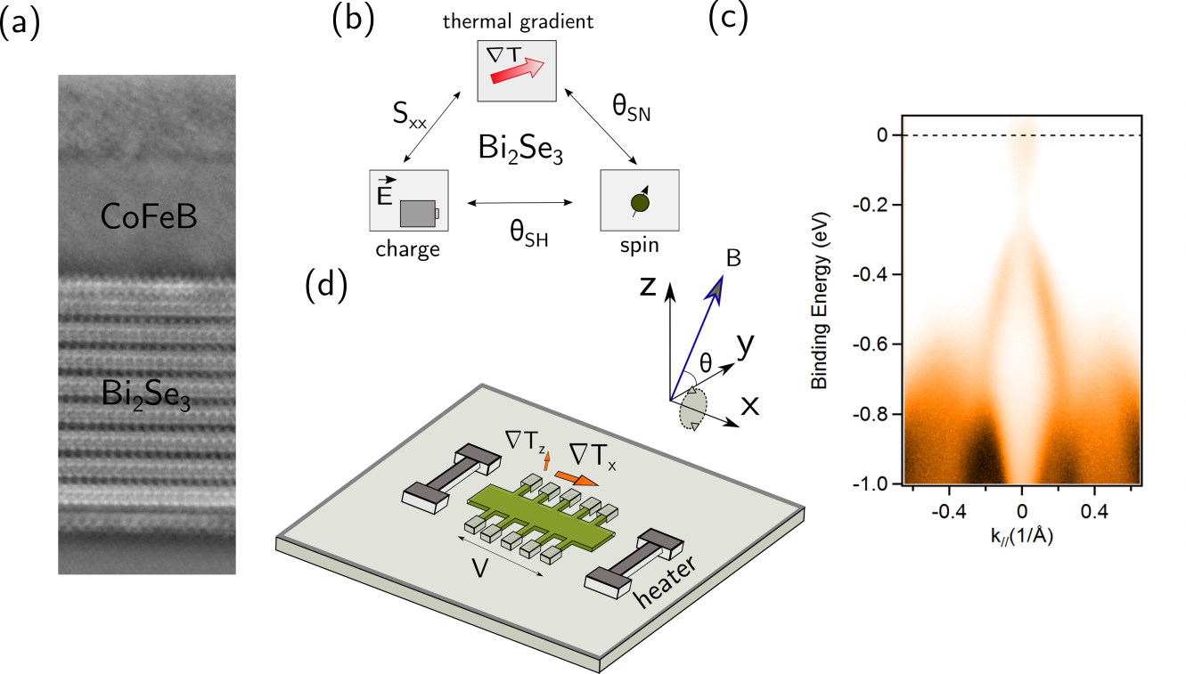
We analyze bilayers of Bi2Se3 (8 nm)/ Co20Fe60B20 ( CoFeB) (5 nm). The 8 nm thickness of the Bi2Se3 was chosen to ensure negligible hybridization between states on the two surfaces [24, 25]. The Bi2Se3 thin films were grown by molecular beam epitaxy and initially capped with 20 nm of Se to protect them from air exposure while transporting them to a separate system for the deposition of the CoFeB. Details about the MBE growth can be found in the supplementary information. High-quality growth of Bi2Se3 is confirmed by atomic force microscopy as well as x-ray diffraction measurements (see Fig. S1). The existence of a surface state on the Bi2Se3 thin films (with no Se cap or CoFeB overlayer) was also confirmed using angle resolved photoemission spectroscopy (ARPES), which measured a Dirac-like dispersion as shown in Fig. 1(c). As is evident from the position of the Fermi-level in Fig. 1(c), the Bi2Se3 layer is electron-doped prior to the Se capping. This is consistent with previous studies which have identified the cause of the doping to be Se vacancies [10]. After transfer to the separate vacuum system we heated the Bi2Se3/Se samples to a heater thermocouple temperature of 285 ∘C for 3.5 hours to remove the Se cap. We then deposited the CoFeB by DC magnetron sputtering followed by a 1.2 nm protective layer of Ta which forms TaOx upon air exposure. Cross-sectional scanning transmission electron microscopy (Fig. 1(a)) shows that the bilayers possess a sharp interface with no visible oxidation at the interface.
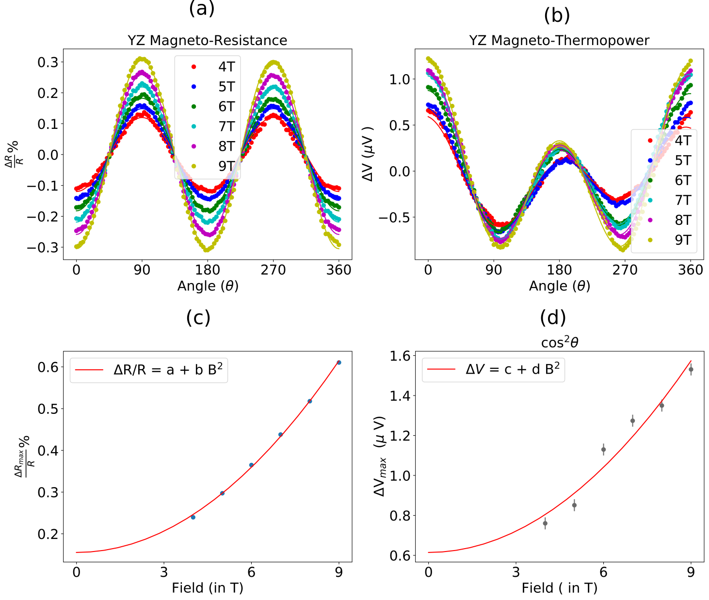
We measure the spin current that is generated both electrically and thermally. As a first step, we measure the spin Hall magnetoresistance of the bilayer. We use optical lithography to pattern a Hall-bar sample geometry with 9 pairs of Hall contacts (only 5 are depicted in Fig. 1(d)) and make a 4-point measurement of the longitudinal resistance while rotating a magnetic field with fixed magnitude in the YZ plane as defined by the diagram in Fig. 1(d). Since the magnetization is always perpendicular to the current flow for this orientation of field sweep, this provides a measurement of the spin Hall magnetoresistance without contamination by the anisotropic magnetoresistance of the magnetic layer. Figure 2(a) shows the magnetoresistance data for magnetic-field magnitudes of 4 to 9 Tesla, large enough compared to the magnetic anisotropy (1.6 Tesla) that to a good approximation the magnetization is saturated along the field direction. The data fit well to the angular dependence . The amplitude of the magnetoresistance for different magnitudes of magnetic field is plotted in Fig. 2(c). We find that the amplitude is well-described by the dependence , where and are constants.
In measurements of separate samples, we find that the YZ magnetoresistance of both an individual Bi2Se3 layer (supplemental Fig. S6(a)) and an individual CoFeB layer (Fig. S6(c)) also have dependences. For the individual Bi2Se3 layer the amplitude of this signal is purely quadratic in with negligible zero-field offset (Fig. S6(b)). For the full bilayer, we therefore identify the contribution that is quadratic in magnetic field (Fig. 2(c)) with the magnetoresistance of the topological insulator and the field-independent component as due primarily to the spin Hall magnetoresistance. The YZ magnetoresistance of an individual CoFeB layer is weak, (Fig. S6(d)) but this is still about 1/5 the value for the full bilayer, so that we take it into account as a small correction to the primary signal (see supplemental material), Assuming that the magnetoresistance of the CoFeB layer and the SMR contribute in parallel to the sample conductance, we estimate for the Bi2Se3/CoFeB bilayer that .
We determine spin Nernst magneto thermopower by measuring the thermal analogue of YZ magnetoresistance, which henceforth we will refer to as the YZ magneto-thermopower. We use the an experimental procedure similar to [26]. We create a thermal gradient along the bilayer Hall bar using a lithographically-defined Pt heater adjacent to one end of the Hall bar, and measure the thermally-induced longitudinal voltage between the forth and last Hall contacts of the bilayer sample. Our samples contain two heaters, one near each end of the Hall bar, so that we can apply in-plane thermal gradients of either sign. For each given heater power, we determine the temperature drop along the sample by measuring the local temperature at the position of the probed pairs of Hall contacts. This is done by measuring the change in the 2-point resistance for each pair of Hall contacts and comparing to measurements of resistance versus temperature when an external heater is used to heat the full sample chip uniformly.
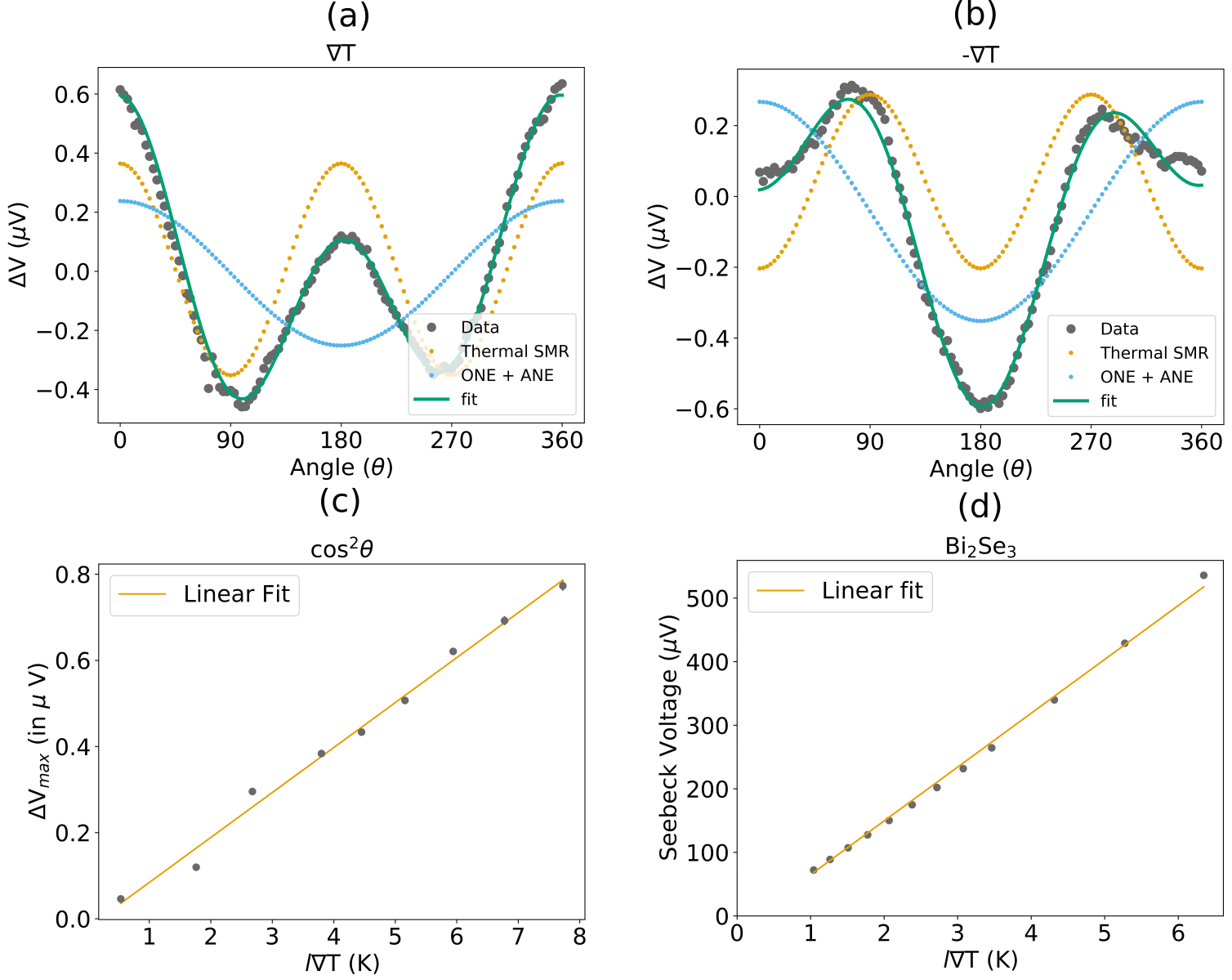
The measured YZ magneto-thermopower of the Bi2Se3 bilayer for magnetic-field magnitudes from 4 to 9 Tesla is shown in Fig. 2(b). Figure 3(a,b) shows a representative analysis of the dependence on magnetic-field angle for two 4 Tesla scans with opposite orientations of in-plane thermal gradients. We observe two distinct contributions to the dependence of the thermopower on magnetic-field angle, and . The contribution can be understood as due to the terms arising for an out-of-plane component of the thermal gradient (Eq. 9). As expected, this contribution retains the same sign when the direction of the in-plane thermal gradient is reversed (compare Fig. 3(a) to Fig. 3(b)).
The component within the YZ magneto-thermopower is our primary focus. Like the magnetoresistance, this component of the magneto-thermopower can be fit to the form with constants and – i.e., it contains a contribution that depends on magnetic-field magnitude due to the Bi2Se3 by itself and a contribution that is independent of the magnetic field magnitude (Fig. 2(c)). We identify the field-magnitude-independent part as due to the spin Nernst effect. For the mm device with a heater power of 442 mW (T = 6.8 0.1 K) we find nV. Figure 3(c) shows (as expected) that the cos term of the YZ magneto-thermopower varies linearly with temperature difference across the device (i.e., for different heater powers).
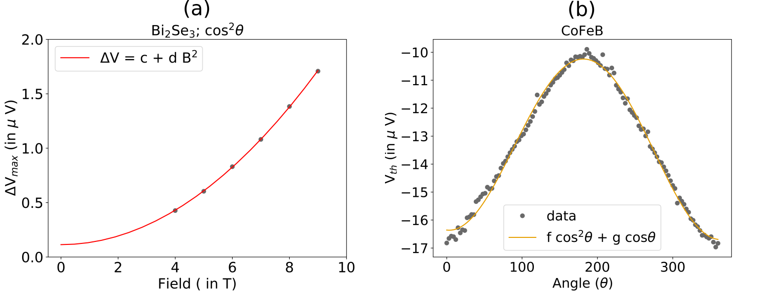
We have checked that the signals corresponding to the spin Nernst thermopower are absent for single layers of either Bi2Se3 or CoFeB. The magneto-thermopower of Bi2Se3 by itself (Fig. 4(a)) has a contribution, but with a field-magnitude-independent part that would be negligible for the bilayer after accounting for shunting. The magneto-thermopower of the CoFeB layer by itself (Fig. 4(b)) contains only a dependence to measurement accuracy, corresponding to the anomalous Nernst voltage with no spin Nernst signal.
To convert our measurement of to the spin Nernst ratio using Eq. 5 we must also determine the absolute Seebeck coefficient and the spin Hall ratio of the Bi2Se3 spin source. To measure the Seebeck coefficient of Bi2Se3, we grew a layer of Bi2Se3 (8 nm) capped with 20 nm of Se, removed the Se with the same process used for the Bi2Se3 samples, and then grew 2 nm of Ta which oxidizes upon air exposure. The Seebeck coefficient was measured using a similar sample geometry as the spin Nernst magneto-thermopower (Fig. 1(d)), but in the absence of a magnetic field. We obtain a Seebeck coefficent for 8 nm Bi2Se3 relative to the Ti(5 nm)/Pt(70 nm) electrodes to be -87 (Fig. 3(d)). The absolute Seebeck coefficient of the electrodes should be small ( -1 [27]), so we estimate that the absolute Seebeck coefficient of the 8 nm Bi2Se3 is with a few percent uncertainty. The measured Seebeck coefficient of the full bilayer is quantitatively consistent using the measured value for the isolated Bi2Se3 layer and the estimated shunting parameter of the bilayer (see supplemental material).
Given our measurements that , , and , Eq. 5 yields the ratio of the spin Nernst ratio to the spin Hall ratio to be . By Eq. 8 the corresponding ratio for the bare spin Nernst ratio is . Values of order 1 for the ratios and have also been measured for heavy metals [19, 15, 16, 26].
To determine the values of , , and by themselves, we must also know the spin Hall ratio for the Bi2Se3 layer. To estimate this quantity, we performed a second harmonic Hall analysis [28] for the Bi2Se3/CoFeB bilayer (see the supplementary information). This analysis yields a spin torque efficiency that is related to according to , where is an interfacial spin transparency factor. We find , which therefore provides a lower bound for . We conclude that a lower bound for is (4.9 0.9) 106 () A m-2 / K m-1, that a lower bound for the magnitude of is approximately , and that a lower bound for the magnitude of is -0.49 0.09. Comparisons to previous measurements of heavy metals are provided in Table 1.
IV Conclusions
In summary, by comparing measurements of the spin Nernst magneto-thermopower in Bi2Se3/CoFeB bilayers to the spin Hall magnetoresistance, we find a lower bound for the magnitude of the spin Nernst ratio for Bi2Se3 of , roughly 3 times greater than that of previously measured values for Pt and 2-3 times greater than that of W. Moreover, the net spin current generated per unit thermal gradient is higher in Bi2Se3 than for W and of a similar magnitude as Pt despite the higher resistivity of Bi2Se3. Interestingly, although the spin Nernst ratio in Bi2Se3 is enhanced relative to the heavy metals, the degree of enhancement appears to be less than for the corresponding spin Hall ratios.
Finally, we address an important question regarding these enhancements in charge/spin and thermal-gradient/spin conversion efficiency: do the topological surface states play a role? The short spin diffusion length in Bi2Se3 [5] suggests that states at the surface must be involved. However, we note that there is currently no known experimental technique that can ascertain whether the topological nature of the surface states shown in Fig. 1(c) survives after the deposition of a metallic ferromagnetic overlayer. Indeed, first principles calculations indicate that the surface states at such interfaces are likely to be complicated [29, 30]. Nonetheless, recent studies have shown that the the density of Berry curvature in the bulk band structure of topological insulators such as Bi2Se3 leads to a large spin Hall conductivity. Bulk-surface correspondence then implies that efficient spin-charge interconversion will also occur via surface states [31].
V Acknowledgements
We thank Steve Kriske for useful suggestions on the experiment and Matthias Althammer and Gaël Grissonnanche for helpful discussions. R.J. grew, fabricated and measured thin films under the supervision of D.C.R with assistance from A.B.; M.S, A.R.R. and T.P. grew the Bi2Se3 films under the guidance of N.S.; X.S.Z. performed Cross-sectional scanning transmission microscopy under the supervision of D.A.M.; R.J and D.C.R. wrote the manuscript with feedback from all authors.
This work made use of the Cornell Center for Materials Research Shared Facilities, which are supported through the NSF MRSEC program (DMR-1719875), and was performed in part at the Cornell NanoScale Facility, a member of the National Nanotechnology Coordinated Infrastructure (NNCI), which is supported by the National Science Foundation (Grant NNCI-2025233). R.J. was supported by US Department of Energy (DE-SC0017671) and A.B. was supported in part by the DOE and in part by the NSF through the Cornell Center for Materials Research (DMR-1719875). We also acknowledge the financial support of the National Science Foundation through the Penn State 2D Crystal Consortium—Materials Innovation Platform (2DCC-MIP) under NSF cooperative agreement DMR-1539916 and DMR-2039351. D.A.M and X.S.Z acknowledge NSF through the Cornell Center for Materials Research (DMR-1719875).
References
- Mellnik et al. [2014] A. Mellnik, J. Lee, A. Richardella, J. Grab, P. Mintun, M. H. Fischer, A. Vaezi, A. Manchon, E.-A. Kim, N. Samarth, et al., Spin-transfer torque generated by a topological insulator, Nature 511, 449 (2014).
- Fan et al. [2014] Y. Fan, P. Upadhyaya, X. Kou, M. Lang, S. Takei, Z. Wang, J. Tang, L. He, L.-T. Chang, M. Montazeri, et al., Magnetization switching through giant spin–orbit torque in a magnetically doped topological insulator heterostructure, Nature Materials 13, 699 (2014).
- Wu et al. [2019] H. Wu, P. Zhang, P. Deng, Q. Lan, Q. Pan, S. A. Razavi, X. Che, L. Huang, B. Dai, K. Wong, et al., Room-temperature spin-orbit torque from topological surface states, Physical Review Letters 123, 207205 (2019).
- Jamali et al. [2015] M. Jamali, J. S. Lee, J. S. Jeong, F. Mahfouzi, Y. Lv, Z. Zhao, B. K. Nikolic, K. A. Mkhoyan, N. Samarth, and J.-P. Wang, Giant spin pumping and inverse spin Hall effect in the presence of surface and bulk spin-orbit coupling of topological insulator Bi2Se3, Nano Letters 15, 7126 (2015).
- Wang et al. [2016] H. Wang, J. Kally, J. S. Lee, T. Liu, H. Chang, D. R. Hickey, K. A. Mkhoyan, M. Wu, A. Richardella, and N. Samarth, Surface-state-dominated spin-charge current conversion in topological-insulator–ferromagnetic-insulator heterostructures, Physical Review Letters 117, 076601 (2016).
- Han et al. [2017] J. Han, A. Richardella, S. A. Siddiqui, J. Finley, N. Samarth, and L. Liu, Room-temperature spin-orbit torque switching induced by a topological insulator, Physical Review Letters 119, 077702 (2017).
- DC et al. [2018] M. DC, R. Grassi, J.-Y. Chen, M. Jamali, D. Reifsnyder Hickey, D. Zhang, Z. Zhao, H. Li, P. Quarterman, Y. Lv, et al., Room-temperature high spin–orbit torque due to quantum confinement in sputtered BixSe(1-x) films, Nature Materials 17, 800 (2018).
- Khang et al. [2018] N. H. D. Khang, Y. Ueda, and P. N. Hai, A conductive topological insulator with large spin Hall effect for ultralow power spin–orbit torque switching, Nature Materials 17, 808 (2018).
- Vineis et al. [2010] C. J. Vineis, A. Shakouri, A. Majumdar, and M. G. Kanatzidis, Nanostructured thermoelectrics: big efficiency gains from small features, Advanced Materials 22, 3970 (2010).
- Hor et al. [2009] Y. Hor, A. Richardella, P. Roushan, Y. Xia, J. Checkelsky, A. Yazdani, M. Hasan, N. Ong, and R. Cava, p-type Bi2Se3 for topological insulator and low-temperature thermoelectric applications, Physical Review B 79, 195208 (2009).
- Guo et al. [2016] M. Guo, Z. Wang, Y. Xu, H. Huang, Y. Zang, C. Liu, W. Duan, Z. Gan, S.-C. Zhang, K. He, et al., Tuning thermoelectricity in a Bi2Se3 topological insulator via varied film thickness, New Journal of Physics 18, 015008 (2016).
- Roschewsky et al. [2019] N. Roschewsky, E. S. Walker, P. Gowtham, S. Muschinske, F. Hellman, S. R. Bank, and S. Salahuddin, Spin-orbit torque and Nernst effect in Bi-Sb/Co heterostructures, Physical Review B 99, 195103 (2019).
- Kim et al. [2020] J.-M. Kim, D.-J. Kim, C.-y. Cheon, K.-W. Moon, C. Kim, P. Cao Van, J.-R. Jeong, C. Hwang, K.-J. Lee, and B.-G. Park, Observation of thermal spin–orbit torque in W/CoFeB/MgO structures, Nano Letters 20, 7803 (2020).
- Bose et al. [2018a] A. Bose, A. S. Shukla, S. Dutta, S. Bhuktare, H. Singh, and A. A. Tulapurkar, Control of magnetization dynamics by spin-Nernst torque, Physical Review B 98, 184412 (2018a).
- Meyer et al. [2017] S. Meyer, Y.-T. Chen, S. Wimmer, M. Althammer, T. Wimmer, R. Schlitz, S. Geprägs, H. Huebl, D. Ködderitzsch, H. Ebert, et al., Observation of the spin Nernst effect, Nature Materials 16, 977 (2017).
- Kim et al. [2017] D.-J. Kim, C.-Y. Jeon, J.-G. Choi, J. W. Lee, S. Surabhi, J.-R. Jeong, K.-J. Lee, and B.-G. Park, Observation of transverse spin Nernst magnetoresistance induced by thermal spin current in ferromagnet/non-magnet bilayers, Nature Communications 8, 1400 (2017).
- Bose et al. [2018b] A. Bose, S. Bhuktare, H. Singh, S. Dutta, V. Achanta, and A. Tulapurkar, Direct detection of spin Nernst effect in platinum, Applied Physics Letters 112, 162401 (2018b).
- Bose and Tulapurkar [2019] A. Bose and A. A. Tulapurkar, Recent advances in the spin Nernst effect, Journal of Magnetism and Magnetic Materials 491, 165526 (2019).
- Sheng et al. [2017] P. Sheng, Y. Sakuraba, Y.-C. Lau, S. Takahashi, S. Mitani, and M. Hayashi, The spin Nernst effect in tungsten, Science Advances 3, e1701503 (2017).
- Liu et al. [2012] L. Liu, C.-F. Pai, Y. Li, H. Tseng, D. Ralph, and R. Buhrman, Spin-torque switching with the giant spin Hall effect of tantalum, Science 336, 555 (2012).
- Nakayama et al. [2013] H. Nakayama, M. Althammer, Y.-T. Chen, K.-i. Uchida, Y. Kajiwara, D. Kikuchi, T. Ohtani, S. Geprägs, M. Opel, S. Takahashi, et al., Spin Hall magnetoresistance induced by a nonequilibrium proximity effect, Physical Review Letters 110, 206601 (2013).
- Chen et al. [2013] Y.-T. Chen, S. Takahashi, H. Nakayama, M. Althammer, S. T. Goennenwein, E. Saitoh, and G. E. Bauer, Theory of spin Hall magnetoresistance, Physical Review B 87, 144411 (2013).
- Kim et al. [2016] J. Kim, P. Sheng, S. Takahashi, S. Mitani, and M. Hayashi, Spin Hall magnetoresistance in metallic bilayers, Physical Review Letters 116, 097201 (2016).
- Zhang et al. [2010] Y. Zhang, K. He, C.-Z. Chang, C.-L. Song, L.-L. Wang, X. Chen, J.-F. Jia, Z. Fang, X. Dai, W.-Y. Shan, et al., Crossover of the three-dimensional topological insulator Bi2Se3 to the two-dimensional limit, Nature Physics 6, 584 (2010).
- Neupane et al. [2014] M. Neupane, A. Richardella, J. Sánchez-Barriga, S. Xu, N. Alidoust, I. Belopolski, C. Liu, G. Bian, D. Zhang, D. Marchenko, et al., Observation of quantum-tunnelling-modulated spin texture in ultrathin topological insulator Bi2Se3 films, Nature Communications 5, 1 (2014).
- Bose et al. [2022] A. Bose, R. Jain, J. J. Bauer, R. A. Buhrman, C. A. Ross, and D. C. Ralph, Origin of transverse voltages generated by thermal gradients and electric fields in ferrimagnetic-insulator/heavy-metal bilayers, Physical Review B 105, L100408 (2022).
- Kockert et al. [2019] M. Kockert, R. Mitdank, A. Zykov, S. Kowarik, and S. Fischer, Absolute Seebeck coefficient of thin platinum films, Journal of Applied Physics 126, 105106 (2019).
- Hayashi et al. [2014] M. Hayashi, J. Kim, M. Yamanouchi, and H. Ohno, Quantitative characterization of the spin-orbit torque using harmonic Hall voltage measurements, Physical Review B 89, 144425 (2014).
- Zhang et al. [2016] J. Zhang, J. P. Velev, X. Dang, and E. Y. Tsymbal, Band structure and spin texture of Bi2Se3 3d ferromagnetic metal interface, Physical Review B 94, 014435 (2016).
- Hsu et al. [2017] Y.-T. Hsu, K. Park, and E.-A. Kim, Hybridization-induced interface states in a topological-insulator–ferromagnetic-metal heterostructure, Physical Review B 96, 235433 (2017).
- Wang et al. [2019] H. Wang, J. Kally, C. Şahin, T. Liu, W. Yanez, E. J. Kamp, A. Richardella, M. Wu, M. E. Flatté, and N. Samarth, Fermi level dependent spin pumping from a magnetic insulator into a topological insulator, Physical Review Research 1, 012014 (2019).
| Bi2Se3 | W | Pt | ||||
|---|---|---|---|---|---|---|
| This work | [26] | [19] | [16] | [15] | [16] | |
| 0.11 | - | 0.2 | 0.32 0.1 | 0.2 | 0.18 0.06 | |
| (A m-2/K m-1) | (4.9 0.9) 106 | - | 1.84 106 | (2.6 0.8) 106 | 1.21 106 | (6 2) 106 |
| 0.15 | 2.4 0.6 | 0.7 | 1.53 0.47 | 0.6 | 1.8 0.6 | |
| 0.73 | - | 0.21 | 0.11 | 0.1 | ||
| SSS () | 4.5 | 12 | 2.6 | 10 | ||
| () | 1064 | 204 | 130 | 125 | 43 | 30 |