Loss and decoherence at the quantum Hall - superconductor interface
Abstract
We perform a systematic study of Andreev conversion at the interface between a superconductor and graphene in the quantum Hall (QH) regime. We find that the probability of Andreev conversion from electrons to holes follows an unexpected but clear trend: the dependencies on temperature and magnetic field are nearly decoupled. We discuss these trends and the role of the superconducting vortices, whose normal cores could both absorb and dephase the individual electrons in a QH edge. Our study may pave the road to engineering future generation of hybrid devices for exploiting superconductivity proximity in chiral channels.
Combining superconductors and quantum Hall (QH) systems has been proposed as a particularly promising direction for creating novel topological states and excitations Mong et al. (2014). Over the past few years, significant progress has been achieved in developing such hybrid structures Rickhaus et al. (2012); Komatsu et al. (2012); Wan et al. (2015); Amet et al. (2016); Lee et al. (2017); Park et al. (2017); Sahu et al. (2018); Matsuo et al. (2018); Kozuka et al. (2018); Seredinski et al. (2019); Zhao et al. (2020); Gül et al. (2022); Hatefipour et al. (2022). In particular, hybridization of QH edge states across a narrow superconducting wire is expected to create a gapped topological superconductor Clarke et al. (2014); Lee et al. (2017). In the fractional QH systems, the strong interactions potentially fractionalize Majorana fermions into parafermions Clarke et al. (2013); Gül et al. (2022), a key ingredient for universal topological quantum computing Mong et al. (2014) and exotic circuit elements such as fractional charge transistors Clarke et al. (2014).
At the interface between a superconductor and a QH system, the QH edge states are expected to be proximitized, turning into chiral Andreev edge states (CAES). These are dispersive states which hybridize the electron and the hole amplitudes Hoppe et al. (2000). An electron approaching the superconducting region is converted to a linear combination of CAES, which interfere as they propagate along the interface. The outgoing particle can either stay as an electron or turn into a hole. We have previously observed clear evidence of the electron-hole conversion in the quantum Hall devices with superconducting contacts Zhao et al. (2020). However, the exact mechanism of this conversion remains open: the role of the disorder, superconducting vortices, and the exact nature of the CAES in this system have been discussed. It is known that in order to observe a strong Andreev conversion in an ideal system a precise matching between the superconductor and the QH edge state momenta is required Giazotto et al. (2005); Akhmerov and Beenakker (2007); van Ostaay et al. (2011); Michelsen et al. (2023). However, the presence of disorder is expected to relax this constraint Manesco et al. (2022); Kurilovich et al. (2023). Vortices in the superconductor and extra QH channels induced by doping could also modify the signal Kurilovich et al. (2023); Tang et al. (2022); Manesco et al. (2022); David et al. (2023). In particular, the normal cores of the vortices can absorb the electrons and holes, reducing the amplitude of the measured signal Zhao et al. (2020); Kurilovich et al. (2023); Schiller et al. (2023).
To address the microscopic mechanisms affecting the Andreev conversion, here we perform a systematic study of the conversion probability vs temperature, , magnetic field, , and interfacial length, . We find that the dependence of the electron-hole conversion probability on magnetic field and temperature nearly factorizes. We suggest a simple phenomenological expression involving exponential decays as a function of , and , and a prefactor determined by the configuration of superconducting vortices. The expression captures the observed dependencies very well, and can be interpreted in terms of the CAES loss and decoherence. We finally discuss the distribution of the Andreev conversion probability Kurilovich et al. (2023), which is unexpectedly found to have a roughly triangular shape. We discuss the implications of our findings for the future development of the more complex devices, which will further explore the physics of superconducting correlations in the chiral states.
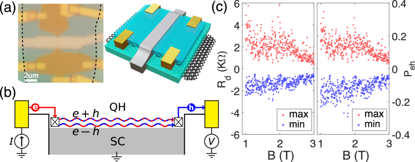
The main device studied here is a hBN/graphene/hBN heterostructure in contact with both superconducting and normal electrodes (Fig. 1a). The superconducting electrode (light gray) is made of sputtered Mo-Re alloy (50-50 in weight) with a critical temperature 10 K and an upper critical field exceeding 12 T. The work function of the alloy 4.2 eV Hałas et al. (2008) is slightly lower than that of graphene 4.5 eV Liang and Ang (2015), resulting in an n-doped graphene region nearby. The graphene sheet is separated into two independent regions by the etching step that defines the superconducting electrode. The widths of the resulting superconductor-graphene interfaces are 0.5 and 1 m. The normal contacts (yellow) are thermally evaporated Cr/Au. The electron density inside the graphene is controlled by applying a voltage to the graphite gate which spans the whole area underneath the heterostructure. While such graphite gates are known to efficiently screen the disorder potential, the results here are similar to our previous measurements of samples without the graphite gate. This indicates that the observed physics is not strongly influenced by the disorder in the graphene layer.
We measure the nonlocal resistance downstream of a grounded superconducting contact, , as sketched in Fig. 1b and demonstrated in the supplementary sup . The CAES formed by the superconductor travel along the interface and recombine into either an electron or hole (or their linear combination) at the end of the interface. Sweeping the gate voltage on top of the QH plateau tunes the momentum difference between the interfering CAES and produces an oscillating pattern of (Fig. S1 in sup ) Zhao et al. (2020). Due to the disordered nature of the interface, these interference patterns are highly irregular and resemble the universal conductance fluctuations Manesco et al. (2022); Kurilovich et al. (2023). Throughout the paper we analyze the statistical properties of these patterns.
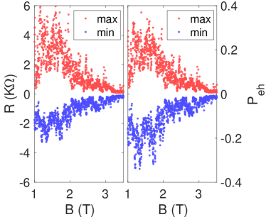
We further convert into the difference between the probabilities of normal and Andreev reflections, , where () is the probability of an electron (or a hole) to be emitted downstream of the superconductor. It is straightforward to show that , where is the Hall resistance Zhao et al. (2020). Note that the extreme values of are reached either for the pure electron reflection (, and , the interface is effectively fully opaque), or for perfect Andreev conversion (, , , a Cooper pair is transferred across the interface per incoming electron). We therefore expect that the distribution of should be skewed toward positive resistances.
Indeed, this skewness can be observed by studying an imbalance between the maximum and minimum values of the downstream resistance . We extract these quantities in the range corresponding to the plateau for a given field and then plot and as a function of in Fig. 1c. The field changes the vortex configuration every few mT Zhao et al. (2020), thereby allowing us to sample multiple different patterns of . The data clearly shows that is on average larger than . The apparent imbalance between electrons and holes is eliminated by converting to in Fig. 1c. (See Fig. S3 in sup for the similar result measured in another device.) We conclude that the probabilities of an electron or a hole being emitted downstream ( and ) are very similar. From now on, we present in lieu of .
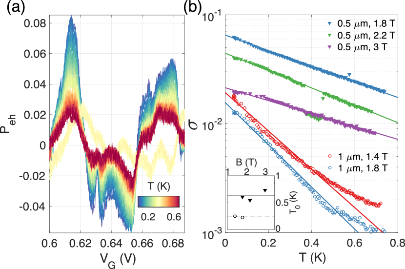
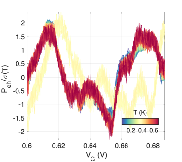
Depending on the length of the interface, the highest electron-hole conversion efficiency we observe is about 0.2 – 0.3. While being very high, this value is still far from reaching unity. Thermal smearing, decoherence and tunneling into the normal vortex cores can all contribute to this suppression. Since at zero temperature only the effect of the vortices remains, we first look into the dependence of on temperature. Fig. 2a plots of the shorter interface (0.5 m) measured over the 2 plateau at 2.2 T from 40 mK to 670 mK. As the temperature increases, gradually decays towards zero, except around 400 mK where the traces briefly jump to a completely different oscillation pattern. We attribute this jump to a temporary change of the configuration of superconducting vortices during the measurement.
To get a quantitative understanding of the thermal effects, we plot the standard deviation of the traces, , as a function of temperature in Fig. 2b for both interfaces at various magnetic fields. The filled triangles (open circles) represent 0.5 m (1 m). The green triangles correspond to the data in Fig. 2a. We find an exponential decay of as a function of temperature, i.e. , where is the decay constant. Remarkably, follows roughly the same decay rate for a given interface length. Even the curves of Fig. 2a which experienced a random jump follow the same slope. (Note the few green symbols nearly overlapping with the purple ones around 0.4 K.) This means that the configuration of superconducting vortices does not have a strong influence on the temperature dependence, even if it dramatically affects the amplitude and the pattern of fluctuations!
The exponential decay is observed regardless of the length of the interface and the magnetic field. For the longer interface, the decay rate becomes less steep at higher temperatures, but only as the signals approach the noise floor of a few , so we extract the slope from the low-temperature range. In the inset of Fig. 2b, we plot the resulting vs. for 0.5 and 1 m. It is clear that does not show any strong dependence on and scales inversely with .
In principle, the exponential temperature dependence could originate from the averaging over energy, like the thermal smearing of oscillations in a QH Fabry-Perot interferometer. However, the effects of thermal smearing are expected to saturate below , while we observe an exponential decay down to temperatures more than 10 times lower (for the shorter interface). Moreover, thermal smearing is predicted to be rather inefficient in this system Kurilovich et al. (2023), because Andreev conversion is only weakly energy dependent. Furthermore, thermal broadening would smear the fluctuations of over . Instead, we observe that the fluctuations in Fig. 2a uniformly decay with temperature with no noticeable smearing. In fact, we show that curves in Fig. 2a could be rescaled to nearly match (see Fig. S5 in sup ).
We therefore ascribe the temperature decay of to the decoherence of the CAES. Indeed, decoherence resulting in the exponential suppression of the oscillations has been measured in Mach-Zehnder interferometers Ji et al. (2003); Roulleau et al. (2008). However, the coherence length of the QH interferometers usually exceeds the length of the superconducting contact by more than an order of magnitude, including our own measurements using similar graphene samples Zhao et al. (2022). The rapid decoherence of the CAES as compared to the QH edge states is likely due to their hybrid nature: The electron and the hole components should acquire an opposite phase in the fluctuating electrostatic potential. The source of these fluctuations could be the gate, or the vortex cores, which serve as a reservoir of normal electrons located next to the CAES.
Since is not strongly affected by the magnetic field and the jumps of the vortex configuration, the effects of the vortices should be primarily encoded in the zero temperature value of . The base temperature of 40 mK allows us to use the corresponding values of as a close approximation to zero temperature value. In the following section, we study the dependence of this quantity on the magnetic field.
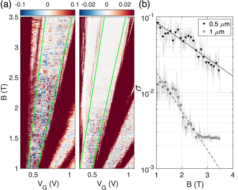
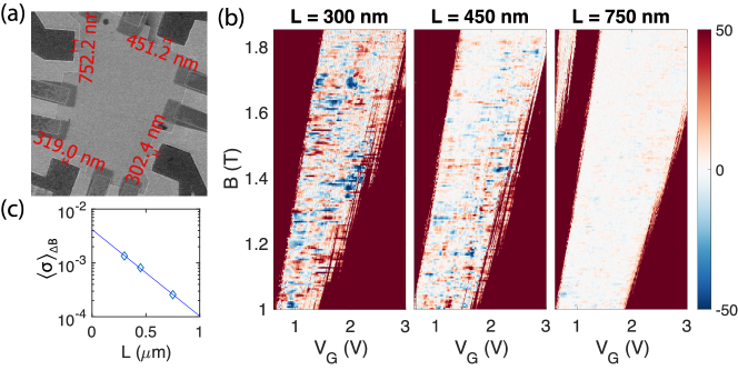
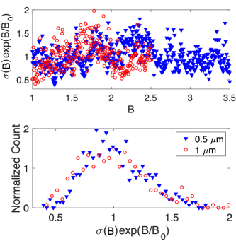
In Fig. 3a we show the patterns of over a wide range of magnetic field for the 0.5 m interface (left) and the 1 m interface (right). A corresponding Hall conductance map is shown in Fig. S2 sup . The boundaries of the 2 plateau are labeled by the green lines. The amplitude of for the longer interface is not only smaller but also decays much faster with increasing . This is consistent with our picture of electrons/holes tunneling from the edge state into the normal cores of the superconducting vortices. Indeed, the probability grows with both and the vortex density, which increases with .
While the dependence of on is highly stochastic (Fig. 1c & S6 in sup ), we can analyze the large-scale trend by averaging over a relatively small range of magnetic fields, mT. The resulting quantity averages over multiple vortex configurations and will be denoted by . As shown in Fig. 3b, it roughly follows an exponential decay with for both interfaces. Excluding the points that reach the noise floor, an exponential fit produces 1.84 T for 0.5 m and 0.85 T for 1 m, in agreement with the expected relation .
Note that this relation further implies an exponential decay of as a function of , with at zero temperature. This dependence indicates that the electrons/holes are efficiently absorbed by multiple vortices, so that the inverse decay length is proportional to the vortex density Kurilovich et al. (2023). The dependence is directly confirmed in another device with three contacts of different interface length, as shown in Fig. S4 sup . Interestingly, both devices have similar in the nm range at 1.5 T.
To summarize the observed trends, we can write
| (1) |
where prefactor represents fluctuations on the scale of a few mT due to vortex rearrangements. Importantly the decay rate is mostly independent of , and is mostly independent of (see Fig. 2b), which supports our assertion that different mechanisms are responsible for the and dependencies.
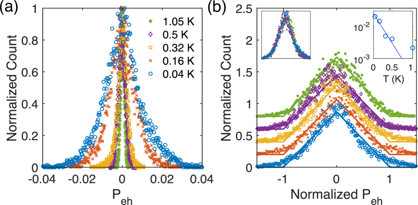
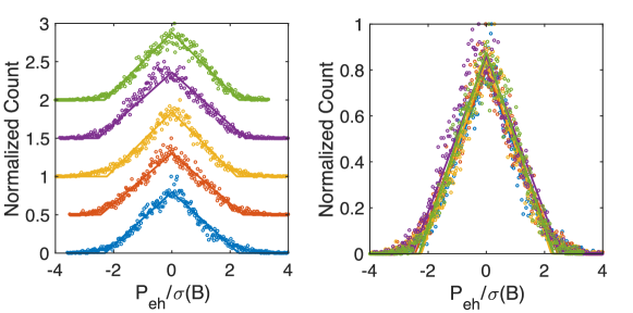
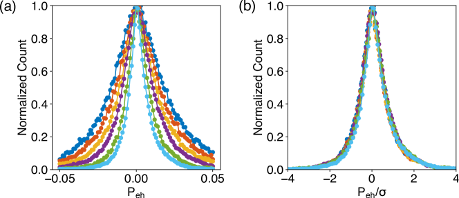
So far we have only considered the standard deviation of , but it is informative to further look into its full distribution. In Fig. 4a we plot the histogram of of the m interface over a small range of T. The range mT is selected because on the one hand it covers many vortex rearrangements; on the other hand mT T so that the systematic reduction of the amplitude is negligible. The measured histogram is clearly peaked around zero, which contrasts with the uniform (rectangular) distribution predicted in Ref. Kurilovich et al. (2023).
While the distribution gets narrower with increasing temperature, the shape remains roughly the same, as seen in Fig. 4b, which replots the histograms with the x-axis normalized by their widths. These widths are plotted in the right inset of Fig. 4b (circles), together with an exponential line whose slope is determined by the constant obtained from Fig. 2b. The decay of the distribution widths with temperature agrees with the line, except for the highest temperature, which is likely limited by the noise in determining .
The distribution shape is expected to be influenced by the positions of the vortices, resulting in the random spread of (see Fig. 1c & S6 in sup ). To evaluate and eventually eliminate the variations of the due to vortex rearrangements, we normalize each trace by its standard deviation calculated for the same . The resulting histograms of are shown in Fig. S7 sup and appear to have a roughly triangular shape similar to those in Fig. 4. We conclude that vortex rearrangements, while quite noticeable, cannot explain the shape of the distribution.
In principle, the non-rectangular distribution of may point to factors that have not yet been fully understood: spin-orbit coupling, interface transparency, contact doping, or specifics of graphene band structure. In particular, if the Andreev conversion probabilities for the two spins states are sufficiently different, the convolution of their rectangular distributions would produce a triangle. Regardless of these mechanisms, the distribution of the should be strongly shaped by the particle losses. In the supplementary sup , we present a toy model which qualitatively reproduces the observed distribution (Fig. S8). In the model, the CAES propagation along the interface is represented by the evolution of a electron/hole density matrix, represented by a trajectory on the Bloch sphere Kurilovich et al. (2023). The key insight of the model is that the losses have uneven effect on different trajectories: Most of the trajectories undergo heavy losses, resulting in a small that contributes to the center of the distribution peak. The rare trajectories which suffered less losses contribute to the tails of the distribution.
In summary, we have reported a systematic investigation of the Andreev conversion probability for the CAES states propagating along a superconducting contact in the QH regime. The main result is the near decoupling of the dependencies on the temperature and magnetic field, i.e. Eq. 1. The dependence on magnetic field, describes the particle loss, where the characteristic field decays with the interface length in agreement with the theoretical prediction Kurilovich et al. (2023). It is natural to associate the temperature dependence, , with decoherence, which is found to be much more efficient compared to the conventional edge states in quantum Hall interferometers. Indeed, the relative phase of the electron and hole components of the CAES should be strongly influenced by the fluctuations of electric environment. Understanding and controling the loss and decoherence processes is crucial for the development of future devices that utilize superconducting correlations in chiral states.
Acknowledgements.
We greatly appreciate stimulating discussion with A. Akhmerov, H. Baranger, L. Glazman, V. Kurilovich, A. Manesco, Y. Oreg, E. Sela, and A. Stern. Sample fabrication and characterization by L.Z. and E.A. were supported by NSF award DMR-2004870. Transport measurements by L.Z. and T.L. and data analysis by L.Z., Z.I. and G.F. were supported by the Division of Materials Sciences and Engineering, Office of Basic Energy Sciences, U.S. Department of Energy, under Award No. DE-SC0002765. The deposition of MoRe performed by F.A. was supported by a URC grant at Appalachian State University. K.W. and T.T. acknowledge support from the Elemental Strategy Initiative conducted by the MEXT, Japan, (grant no. JPMXP0112101001), JSPS KAKENHI (grant no. JP20H00354) and CREST (no. JPMJCR15F3, JST). The sample fabrication was performed in part at the Duke University Shared Materials Instrumentation Facility (SMIF), a member of the North Carolina Research Triangle Nanotechnology Network (RTNN), which is supported by the National Science Foundation (Grant ECCS-1542015) as part of the National Nanotechnology Coordinated Infrastructure (NNCI).References
- Mong et al. (2014) R. S. K. Mong, D. J. Clarke, J. Alicea, N. H. Lindner, P. Fendley, C. Nayak, Y. Oreg, A. Stern, E. Berg, K. Shtengel, and M. P. A. Fisher, Phys. Rev. X 4, 011036 (2014).
- Rickhaus et al. (2012) P. Rickhaus, M. Weiss, L. Marot, and C. Schönenberger, Nano Letters 12, 1942 (2012).
- Komatsu et al. (2012) K. Komatsu, C. Li, S. Autier-Laurent, H. Bouchiat, and S. Guéron, Phys. Rev. B 86, 115412 (2012).
- Wan et al. (2015) Z. Wan, A. Kazakov, M. J. Manfra, L. N. Pfeiffer, K. W. West, and L. P. Rokhinson, Nature Communications 6, 7462 (2015).
- Amet et al. (2016) F. Amet, C. T. Ke, I. V. Borzenets, J. Wang, K. Watanabe, T. Taniguchi, R. S. Deacon, M. Yamamoto, Y. Bomze, S. Tarucha, and G. Finkelstein, Science 352, 966 (2016).
- Lee et al. (2017) G.-H. Lee, K.-F. Huang, D. K. Efetov, D. S. Wei, S. Hart, T. Taniguchi, K. Watanabe, A. Yacoby, and P. Kim, Nature Physics 13, 693 (2017).
- Park et al. (2017) G.-H. Park, M. Kim, K. Watanabe, T. Taniguchi, and H.-J. Lee, Scientific Reports 7, 10953 (2017).
- Sahu et al. (2018) M. R. Sahu, X. Liu, A. K. Paul, S. Das, P. Raychaudhuri, J. K. Jain, and A. Das, Phys. Rev. Lett. 121, 086809 (2018).
- Matsuo et al. (2018) S. Matsuo, K. Ueda, S. Baba, H. Kamata, M. Tateno, J. Shabani, C. J. Palmstrøm, and S. Tarucha, Scientific Reports 8, 3454 (2018).
- Kozuka et al. (2018) Y. Kozuka, A. Sakaguchi, J. Falson, A. Tsukazaki, and M. Kawasaki, Journal of the Physical Society of Japan 87, 124712 (2018).
- Seredinski et al. (2019) A. Seredinski, A. W. Draelos, E. G. Arnault, M.-T. Wei, H. Li, T. Fleming, K. Watanabe, T. Taniguchi, F. Amet, and G. Finkelstein, Science Advances 5, eaaw8693 (2019).
- Zhao et al. (2020) L. Zhao, E. G. Arnault, A. Bondarev, A. Seredinski, T. F. Q. Larson, A. W. Draelos, H. Li, K. Watanabe, T. Taniguchi, F. Amet, H. U. Baranger, and G. Finkelstein, Nature Physics 16, 862 (2020).
- Gül et al. (2022) O. Gül, Y. Ronen, S. Y. Lee, H. Shapourian, J. Zauberman, Y. H. Lee, K. Watanabe, T. Taniguchi, A. Vishwanath, A. Yacoby, and P. Kim, Phys. Rev. X 12, 021057 (2022).
- Hatefipour et al. (2022) M. Hatefipour, J. J. Cuozzo, J. Kanter, W. M. Strickland, C. R. Allemang, T.-M. Lu, E. Rossi, and J. Shabani, Nano Letters 22, 6173 (2022).
- Clarke et al. (2014) D. J. Clarke, J. Alicea, and K. Shtengel, Nature Physics 10, 877 (2014).
- Clarke et al. (2013) D. J. Clarke, J. Alicea, and K. Shtengel, Nature Communications 4, 1348 (2013).
- Hoppe et al. (2000) H. Hoppe, U. Zülicke, and G. Schön, Physical Review Letters 84, 1804 (2000).
- Giazotto et al. (2005) F. Giazotto, M. Governale, U. Zülicke, and F. Beltram, Phys. Rev. B 72, 054518 (2005).
- Akhmerov and Beenakker (2007) A. R. Akhmerov and C. W. J. Beenakker, Phys. Rev. Lett. 98, 157003 (2007).
- van Ostaay et al. (2011) J. A. M. van Ostaay, A. R. Akhmerov, and C. W. J. Beenakker, Phys. Rev. B 83, 195441 (2011).
- Michelsen et al. (2023) A. B. Michelsen, P. Recher, B. Braunecker, and T. L. Schmidt, Phys. Rev. Res. 5, 013066 (2023).
- Manesco et al. (2022) A. L. R. Manesco, I. M. Flór, C.-X. Liu, and A. R. Akhmerov, SciPost Phys. Core 5, 045 (2022).
- Kurilovich et al. (2023) V. D. Kurilovich, Z. M. Raines, and L. I. Glazman, Nature Communications 14, 2237 (2023).
- Tang et al. (2022) Y. Tang, C. Knapp, and J. Alicea, Phys. Rev. B 106, 245411 (2022).
- David et al. (2023) A. David, J. S. Meyer, and M. Houzet, Phys. Rev. B 107, 125416 (2023).
- Schiller et al. (2023) N. Schiller, B. A. Katzir, A. Stern, E. Berg, N. H. Lindner, and Y. Oreg, Phys. Rev. B 107, L161105 (2023).
- Hałas et al. (2008) S. Hałas, T. Pieńkos, M. Czarnacki, and T. Durakiewicz, Vacuum 82, 1094 (2008).
- Liang and Ang (2015) S.-J. Liang and L. K. Ang, Phys. Rev. Appl. 3, 014002 (2015).
- (29) See Supplemental Material
- Ji et al. (2003) Y. Ji, Y. Chung, D. Sprinzak, M. Heiblum, D. Mahalu, and H. Shtrikman, Nature 422, 415 (2003).
- Roulleau et al. (2008) P. Roulleau, F. Portier, P. Roche, A. Cavanna, G. Faini, U. Gennser, and D. Mailly, Phys. Rev. Lett. 100, 126802 (2008).
- Zhao et al. (2022) L. Zhao, E. G. Arnault, T. F. Q. Larson, Z. Iftikhar, A. Seredinski, T. Fleming, K. Watanabe, T. Taniguchi, F. Amet, and G. Finkelstein, Nano Letters 22, 9645 (2022).
- Caroli et al. (1964) C. Caroli, P. D. Gennes, and J. Matricon, Physics Letters 9, 307 (1964).
Methods
Device Fabrication
The graphene and hBN flakes are exfoliated onto Si/SiO2 substrates (280 nm thickness) with Scotch Magic tapes and then assembled together using PC/PDMS stamps. The thickness of the hBN flakes are selected to be 30 nm for top layers and 60 nm for bottom layers. The graphite back-gate layers are about 5 to 10 nm thick. The bottom hBN are intentionally chosen thicker to prevent breakdown between the electrodes and the graphite back-gate. The stamps are made by first dripping SYLGARD 184 silicone droplets onto hot glass slides (C) to form PDMS hemispheres and then plasma ashing for 15 mins. We carefully place PC films over the PDMS bases to avoid bubbles in between. The PC films are prepared with PC solution (6% in weight) spread between two glass slides. The stamps are first cured over a hotplate at 180∘C for 20 mins and then cured again over the stamping station upside down right before usage. During the dry transfer process, the ambient temperature is maintained above 90∘C to reduce water contamination. At the last stage, the fully assembled hBN/graphene/hBN/graphite heterostructure is slowly dropped onto a plasma ashed hot (C) Si/SiO2 substrate to drag bubbles out. After removing PC residue in hot chloroform, the sample is annealed in open air at 500∘C over night.
The stack is characterized by AFM and Raman topography. We pattern the device over the identified clean region using e-beam lithography on top of double layer PMMA resist (495K, A4), developed in cold IPA/DI water mixture (3:1 in volume). Right before electrodes deposition, the patterned region is etched by CHF3/O2 (50/5 ccm, 70 W, 100 mtorr) carefully to etch through the top later hBN only. The normal metal electrodes are made of thermally evaporated Cr/Au (1/90 nm) with a base pressure 10-7 torr. The superconducting electrodes are made of MoRe alloy (50-50 in weight) DC sputtered in a high vacuum system (AJA, 10-8 torr).
Measurements
The measurements are performed in an Oxford dilution refrigerator equipped with resistive coax lines together with two-stage low pass LC and RC filters. The total resistance of each filtered line is about 1.7 kOhm and the cut off frequency is around 200 kHz. The nonlocal differential resistances are measured using a 1nA square-wave excitation with home-made preamplifiers and USB-6363. The graphite back-gate voltage is supplied with USB-6363 in series with a 1/4 voltage divider. For consistency, and to reduce sample overheating, the magnetic field ramp direction is always from high to low.
Supplemental Material
Comparison with a non-superconducting interface
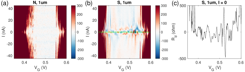
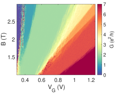
We first verify that the downstream resistance fluctuations originate from the proximity effect of the superconductor instead of other spurious reasons (e.g. non-quantized QH bulk conductance). A careful examination of the signal has been presented in our former work Zhao et al. (2020). To be cautious, we still compare of the superconductor to that of a normal contact of the same interface length in Fig. S1. Indeed, the fluctuating is uniquely present only at the the superconducting interface. In addition, the level of QH quantization can be checked in the data presented in Fig. S2.
Data measured in additional samples
In Fig. S3, we further illustrate the conversion from to similar to that in Fig. 1c.
To test the inferred relation with , we further fabricated another device with 3 different . In Fig. S4 we plot vs. at 60 mK for in the T range (a 10 nA excitation is used for this measurement). Indeed, the dependence on clearly shows an exponential decay with nm.
Uniform temperature dependence of
In Fig. 2a, the curves gradually flatten with increasing temperature, without showing any noticeable broadening. In fact, the curves at different temperatures can be universally scaled by simply normalizing them by their standard deviation: , where is calculated over the range of at the same , Fig. S5. (This excludes the curves in yellow, that jump to a different pattern.) This observation allows us to explore vs. in place of the full in Fig. 2b.
Variation of signal due to rearrangement of vortices
Here we analyze the strong fluctuations of the signal, described by the prefactor in eq. (1). At the lowest temperature, we can take . Qualitatively, the vortex density increases with magnetic field, leading to the losses growing . On top of this trend, the losses randomly change each few mT due to the vortex rearrangements. These variations are described by , which is plotted in the top panel of Fig. S6. The quantity appears to be uniformly distributed in . We plot its histogram in the bottom panel of Fig. S6. The distribution is broad and clearly asymmetric, with most of the counts ranging from 0.5 to 1.5 of the average value.
Histograms of normalized
The distribution of plotted in Fig. 4a is peaked around zero in contrast to the predicted uniform distribution in Ref. Kurilovich et al. (2023). However, a uniform distribution can also be distorted if the distribution of vortex configurations produce a wide spread of (see Fig. S6). To eliminate this effect, we normalize each curve by its standard deviation, , calculated at the same . We plot the histograms of the resulting quantity in Fig. S7. We find that the shape of the distribution remains roughly the same as in Fig. 4a. Therefore, the variation of losses with cannot explain the roughly triangular shape of the distribution.
Toy model for the distribution of
To explain the non-rectangular distribution in Fig. 4 and Fig. S7, we constructed a simple toy model, in which the local state of the CAES is represented by the density matrix, . The CAES propagation along the interface results in random trajectories on the Bloch sphere, which we simulate with the attached code. In the simulation, we assume a random variation of the phase of the order parameter along the interface Kurilovich et al. (2023). We generate multiple realizations of the random superconducting phase to simulate the effect of the vortex rearrangements with . For each realization, we assume that controls the coupling strength between the CAES and the superconductor. We vary this strength thereby generating different trajectories on the Bloch sphere. We take at the final point of the interface, which yields the traces. We verify that without the losses or decoherence, the expected rectangular distribution of is obtained, which corresponds to the uniform random coverage of the Bloch sphere (not shown).
We first model the losses, which we assume to be due to tunneling into zero energy states, e.g. to the Caroli-de Gennes-Matricon states of the nearby vortices Caroli et al. (1964)). We assume that the losses are localized at a few places along the interface corresponding to the random locations of the closest vortices. At a given location along the interface, the loss is maximal at a certain position on the equator of the Bloch sphere, as determined by the local phase of the order parameter. The simulation produces a sharp distribution (blue curve in Fig. S8a), qualitatively similar to those found in the experiment. Analyzing the simulated trajectories, we find that majority of trajectories experience significant losses, resulting in the peak at zero . It is the outlier trajectories which happened to avoid heavy losses that contribute to the tails of the distribution.
We then introduce the dephasing of the standard type, which reduces coherence between the electron and hole components of the density matrix. Keeping the same randomly generated patterns of loss and the phase of the order parameter, we run the simulation for several values of the dephasing. Fig. S8a shows the resulting distributions, which appear qualitatively similar to Fig. 4. The shape of these distributions is also similar to the one obtained in the simulation with pure losses and no dephasing. The similarity of the simulated distributions allows us to rescale them as shown in Fig. S8b, similar to the rescaling of the experimental curves in Fig. S7b.
Given the number of unknown parameters in our toy model, we do not pursue a qualitative agreement with the experiment. Instead, we believe the simulations illustrate the underlying reasons for the unusual shape of the observed histograms of .