Charge distribution and spin textures in magic-angle twisted bilayer graphene
A.O. Sboychakov
Institute for Theoretical and Applied Electrodynamics, Russian Academy of Sciences, Moscow, 125412 Russia
A.V. Rozhkov
Institute for Theoretical and Applied Electrodynamics, Russian Academy of Sciences, Moscow, 125412 Russia
A.L. Rakhmanov
Institute for Theoretical and Applied Electrodynamics, Russian Academy of Sciences, Moscow, 125412 Russia
Abstract
We examine the coexisting spin and charge density waves as a possible ground state of the magic-angle twisted bilayer graphene. When interactions are not included, the spectrum of the material has 4 (8 if spin is taken into account) almost flat almost degenerate bands. Interactions break down the degeneracy forming an order parameter which is usually assumed to be a spin density wave with a preset spin structure. Here we take into account a possible charge density wave contribution to the order parameter, that is, inhomogeneous distribution of the charge density within a twisted graphene supercell. We also calculate self-consistently the spin structure of the order parameter. We find that the density wave order is stable in the whole doping range from to extra electrons per supercell. The spin texture changes from collinear at zero doping to almost coplanar at finite doping. The density wave order shows nematic distortion when we dope the system. We demonstrate that the local spin magnetization is much stronger than the charge density variation, unless the doping exceeds extra electrons or holes per supercell.
In our previous papers OurtBLGPRB2019 ; NematicPRB2020 we assumed the
planar SDW order to be the ground state of the system in the doping range
electrons per supercell. This choice was not arbitrary. It is
known that in the tBLG at small twist angle the electrons at the Fermi
level are located in the AA regions of the superlattice
cell ourBLGreview2016 ; dSPRB . The ground state of the AA stacked
bilayer graphene should be antiferromagnetic
(AFM) AAPRL ; AAPRB2013 .
Based on the assumption of the SDW order, our simulations reproduced
qualitatively well the dependence of the conductivity on the doping
observed experimentally. We also
showed NematicPRB2020
that doping the system away from the charge neutrality point leads to the
formation of the nematic state, which is also detected by the
STM MottNematicNature2019 ; KerelskyNematicNature2019 ; STMNature2019 ; WongNematic2020 .
In the present paper we extend the variety of possible order parameters, considering the non-coplanar SDW order on a backdrop of the inhomogeneous charge distribution. We show that the spin texture changes from collinear to almost coplanar with doping. It is demonstrated that the symmetry of the SDW order is reduced with doping. This leads to the formation of the nematic spin state. At the same time, the rotational symmetry of the charge density is almost unaffected by doping. The nematic state can manifests itself in the non-symmetric spatial distribution of the local density of states, which was observed experimentally MottNematicNature2019 ; KerelskyNematicNature2019 ; STMNature2019 ; WongNematic2020 . Finally, we show that local spin density is much stronger than the charge density variation unless the doping exceeds 3 extra electrons or holes per supercell.
Model Hamiltonian.
The periodic superstructure exists in the tBLG when satisfies the condition
(1)
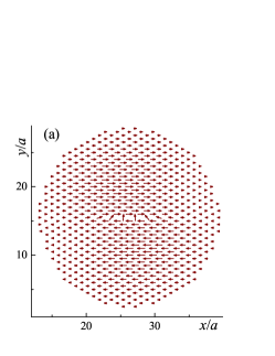
with and being mutually coprime positive integers ourBLGreview2016 . The superlattice cell has a form of a right rhombus. When the superlattice cell coincides with the moiré cell. In our study we consider only such superstructures. When the twist angle is small, the supercell can be considered as consisting of regions with AA, AB, and BA stacking ourBLGreview2016 ; NanoLettTB .
We use the following model Hamiltonian of tBLG:
(2)
Here () are the creation (annihilation) operators of the electron with spin (, ) at the unit cell in the layer () in the sublattice (), while . The first term in Eq. (2) is the single-particle tight-binding Hamiltonian with being the amplitude of the electron hopping from site in the position to the site . The second term in Eq. (2) describes the on-site (Hubbard) interaction of electrons, while the last term corresponds to the inter-site Coulomb interaction (the prime means that the elements with should be excluded).
Now we have to choose a parametrization of the hopping amplitudes. We keep only nearest-neighbor terms for the intralayer hopping with eV. The inter-plane hopping amplitudes are parameterized by the following Slater-Koster formula for electrons
(3)
where is the unit vector transverse to the layers,
(4)
and the cutoff function is introduced to nullify the hopping amplitudes at distances larger than . We use Å, Å. The parameter defines the largest interlayer hopping amplitude. We choose eV (this value was used to describe the AB bilayer graphene ourBLGreview2016 ). The parameter describes how fast the hopping amplitudes decay inside the region . We choose Å.
At the first magic angle the low-energy band structure
consists of 4 almost flat almost degenerate bands separated by energy gaps
from lower and higher dispersive bands. The bandwidth of these flat
bands has a minimum at . For model parameters used here
we numerically determine that
meV, the gaps between flat and dispersive bands are meV, and (which is close to the experimentally observed and corresponds to the superstructure with and ).
Spin and Charge Densities.
When the system has flat bands crossing the Fermi level, the interactions
become very important. The interactions break the symmetry of the single
particle Hamiltonian inducing some order parameter. We start with the
SDW-like ordering, with multicomponent order parameter. First, we introduce on-site order parameters
(5)
The quantity is complex, while is real. They describe on-site magnetization
(6)
Parameters and are controlled by the Hubbard interaction. We take . This value is somewhat smaller than the critical value for a single-layer graphene transition into a mean-field AFM state MF_Uc_sorella1992 , . Thus, our Hubbard interaction is rather strong, but not too strong to open a gap in single layer graphene.
In a graphene layer, each atom in one sublattice has three nearest neighbors belonging to another sublattice. For this reason we consider three types of in-plane nearest-neighbor order parameters of the SDW type, and (), corresponding to three different links connecting the nearest-neighbor sites. These order parameters are defined as follows
(7)
where
,
,
,
,
and
is the in-plane nearest-neighbor Coulomb repulsion energy
(
is the vector connecting
and
sites in the graphene unit cell). We take
,
in agreement with Ref. Wehling . The order parameters (7) define spins on links connecting in-plane nearest neighbor sites according to
where is a vector of the Pauli matrices. In contrast to Ref. NematicPRB2020 , the spins and are allowed to have the components. In Ref. NematicPRB2020 we also considered
inter-layer nearest-neighbor SDW order parameters. The calculations showed, however, that these components are by order of magnitude smaller than (which are smaller than
). In present paper we neglect such order parameters.
Besides the SDW order parameters, we consider here the charge-density-wave-like contributions. First, we take into account that the charges are not uniformly distributed inside the superlattice cell and introduce the quantity
(9)
This value can be considered as the on-site potential due to charge inhomogeneity. Note that is finite even in the absence of any symmetry breaking since the sites inside a supercell are non-identical. Thus, it cannot be considered as an order parameter. In our simulations is normalized according to
(10)
where is the number of supercells in the system, and is the doping level, that is, the number of extra electrons or holes per one supercell. Besides , we introduce the in-plane nearest-neighbor (inter-site) potentials
(11)
For all these charge and spin distributions we assume the same periodicity as the supercell periodicity.
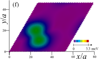
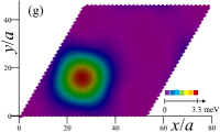
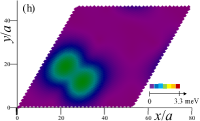
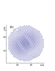
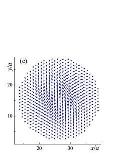
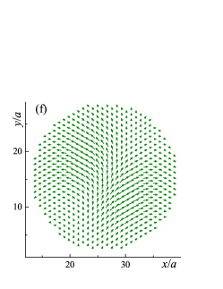
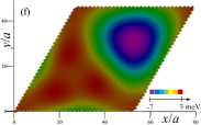
Figure 1: The spatial distribution of the order parameters [(a), (e)] and [ (b) – (d) and (f) – (h)] (for definition, see the text) calculated at [(a) – (d)] and [(e) – (h)]. Doping reduces the symmetry of the order parameters from down to .
Mean-field iteration scheme.
To calculate the order parameters and potentials, we use a mean-field approach. It is based on the decoupling of the quadratic terms in the Hamiltonian (2):
As a result, we obtain a mean-field Hamiltonian . Numerical algorithm for finding the order parameters and the potentials is similar to that used in Ref. NematicPRB2020 . First, we write down the electronic operators in the momentum representation PankratovPRB2013
(13)
where is the number of the graphene unit cells in one layer of the sample, is the position of the -th unit cell of the -th layer, the momentum lies in the first Brillouin zone of the superlattice, and are the reciprocal vectors of the superlattice lying in the first Brillouin zone. The number of vectors is equal to for each graphene layer.
The mean-field Hamiltonian is matrix, where (factor is due to the spin, layer, and sublattice indices). The rank of this matrix is too large to perform numerical integration over the quasimomentum for a realistic time. Indeed, for the first magic angle we have . For this reason, we use simplifications. The main contribution to the order parameters comes from the low-energy states. Consequently, the contributions from other states can be approximated. In the limit of uncoupled () graphene layers and zero order parameters, the matrix is block-diagonal with the matrices on its diagonal
(14)
where , are the unit vectors of the -th layer. The eigenenergies of such a matrix are . The interlayer hopping amplitudes and order parameters are much smaller than . As long as we are interested in low-energy features, we can use the truncated matrix excluding the rows and columns in containing elements with , where is the cutoff energy. The rank of the truncated matrix is . The eigenenergies of , which lie close to , are calculated with significant errors. To fix this problem, we take into account only bands with , where . The number of such bands is . We use , (, ). Calculations with smaller and larger and show that the results are almost independent of these quantities.
The contribution to the total energy from the discarded states
must be accounted for separately. Since is much larger than order parameters, this can be done perturbatively. The leading corrections to the total energy are quadratic in SDW order parameters ,
,
,
and
.
We assume that the proportionality coefficients are identical for all order parameters and are equal to
(15)
where
is the single-layer graphene density of states. Such a correction can be taken into account by the replacement in the mean-field Hamiltonian
(16)
where is the Hamiltonian in the truncated basis. The contributions to and from the bands with are almost independent of the interactions and ordering. In the limit of uncoupled layers and zero order parameters, the contribution to from each excluded band equals . As a result, we obtain the self-consistency condition for
(17)
where are eigenfunctions of
, is the step function, is the
area of the supercell’s Brillouin zone, and is the chemical
potential. The summation in Eq. (17) is performed over
bands and truncated basis, and the equation for chemical potential is
(18)
Figure 2: The on-site spins
in sublattice (a) and
(b) at . Spins lie in the plane. For the purpose of
the visual representation, the rotation of the spins from plane to
plane is performed. Only AA region of the supercell is shown.
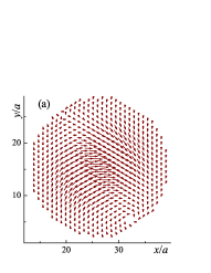
Figure 3:
The textures of spins on the link,
,
calculated at . Panels (a) – (c) show the projections of the
spins for different values of link parameter
,
while panels (d) – (f) depicts the projections (after rotation to
the plane). Only AA region of the supercell is shown.
The contribution to from excluded bands is non-zero
(moreover, one can check that it is non-zero even for single-layer graphene). In the limit of uncoupled layers this contribution is independent of and . Thus, one can write , where
can be estimated as
(19)
where , and is
independent of . For parameters chosen, we have
. The parameter renormalizes the
in-plane nearest-neighbor hopping amplitude .
We assume that this renormalization is already absorbed into the value
eV,
and thus can be ignored.
As for , we add quadratic term to the effective Hamiltonian, similar to that in Eq. (16).
To calculate the order parameters and the potentials we minimize the total
energy iteratively using the method of successive
approximations. In each iteration, we calculate and
of the matrix
, and the gradients
,
where
,
,
,
,
or .
These gradients are used to calculate new values of the aforementioned
quantities. New value of
is found using
Eq. (17) with from Eq. (18).
Results.
Our numerical calculations reveal that the SDW order exists in the system at any doping level. However, the spatial distributions of the SDW magnetization are qualitatively different for different .
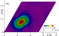
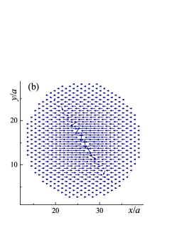
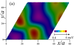
Let us start from . Figures 1(a) – (d) depicts the spatial distributions of
and
inside the superlattice cell for
.
These quantities describe the absolute values of the on-site spins and spins on the links, correspondingly. We see that the order parameters are non-zero only in the AA region. At zero doping, the order parameters spatial distributions have rather symmetric form. The area of non-zero has a shape of a ‘rounded’ hexagon. This hexagon is invariant under rotation on around the center of the AA region , with being the elementary vectors of the superlattice. Figures 1(b) – (d) demonstrate that spin magnetization on the links remain finite within the areas shaped like a dumbbell. The rotation on
and also on around preserves .
When all spins, and , are collinear. For layer , all on-site spins of the sublattice point along axis, while in the sublattice they have the opposite direction. The same is true for layer . Therefore, the on-site spin texture has the collinear AFM arrangement. The spins on the links
also form a kind of AFM structure: in one part of the dumbbell directed along axis, while in another part of the dumbbell they have the opposite direction.
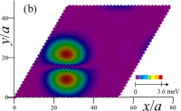
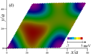
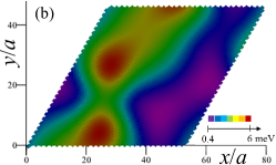
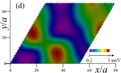
Figure 4:
The spatial distribution of the on-site potential
[(a), (e)],
[(b), (f)],
[(c), (g)], and
[(d), (h)], calculated at [(a) – (d)] and at
[(e) – (h)].
The order parameters distributions change with doping. In Fig. 1(e) – (h) we plot the spatial distribution of and at hole doping . We see that now no hexagonal symmetry exists. The profile of is stretched unidirectionally, and rotation is no longer a symmetry of . However, all these order parameters are symmetric under rotation on . In doped systems the spin textures are no longer collinear. The on-site spins turn out to be coplanar. We believe that this is not an artifact since our numerical procedure accounts for non-coplanar textures. In our simulations the on-site spins lie in the plane (see Fig. 2), they form a helical AFM structure. The spins on links, , form a non-coplanar structures. However, almost all of these spins lie in the plane, and only small fraction of them have components. Figures 3(a) – (c) show the directions of spins projected to the plane, while Figs. 3(d) – (f) show the directions of spins projected to the plane (with subsequent rotation to the plane). We see that almost all spins lie in the plane. The spins which violate the coplanarity lie along three lines passing through the center of the AA region. These lines are visible in Fig. 3(a) – (c).
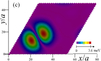
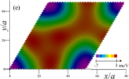
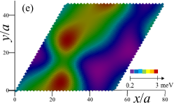
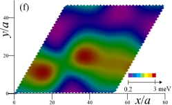
Figure 5:
The spatial distribution of the inter-site potentials for three different , calculated at x=0 [(a) – (c)] and at [(d) – (f)].
In Fig. 4 we plot the spatial distributions of the on-site potential calculated at zero doping [panels (a) – (d)] and at [panels (e) – (h)]. The distributions are shown for each layer and sublattice separately. At there is an excess of electrons in the AA region and lack of electrons in the AB (corners of the supercell) and BA (area centered at ) regions of the superlattice cell. At , the area, where excess of electrons is observed, expands; extra electrons also appear in the AB (for and ) and BA (for and ) regions. At zero doping the charge distributions remain invariant under rotation on around the point . The potentials and are transformed into each other under the rotation on around the point . The same is true approximately at . Thus, the nematicity does not manifest itself through the charge distribution.
Figure 5 shows the spatial distributions of the inter-site potentials , calculated at and . The profiles of are approximately the same for and , and only absolute values of change. These spatial distributions are approximately symmetric under rotation on around . The inter-site potentials are transformed into each other under the rotation on around the point .
Thus, the doping reduces the symmetry of the SDW order from
,
which is the symmetry of the lattice, to
indicating the appearance of the nematic
state NematicPRB2020 .
At the same time the symmetry of the charge-related quantities
and
is virtually unaffected by doping. These parameters are integrated
quantities that are influenced by contributions of high-energy states, the
latter being insensitive to the low-energy symmetry breaking. At the same
time, the electron nematic state can manifest itself as a symmetry
reduction of the local density of states, which can be detected in an STM
experiment. This is confirmed by our simulations.
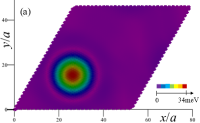
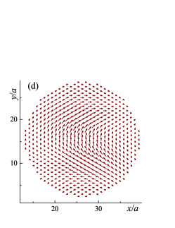
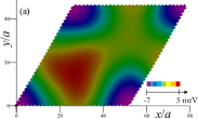
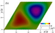
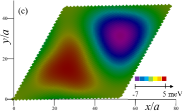
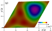
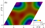
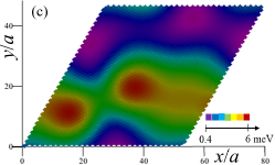
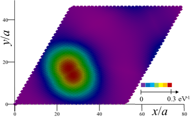
Figure 6
shows the spatial distribution of the local density of states calculated
close to half filling (at
the density of states is almost zero). The spatial profile is stretched
indicating the appearance of the nematic state. Such a feature was observed
in the
experiments MottNematicNature2019 ; KerelskyNematicNature2019 ; STMNature2019 ; WongNematic2020 .
Finally, we compare the values of the spin and charge density variations. At zero doping, the on-site spin order parameter reaches the maximum about meV. At the same time, the on-site charge density variation is about times smaller. The SDW order parameters decrease down to zero, when the doping changes from to . At the same time, the values of do not change much with . However, even at the maximum value of is about times larger than that of , and only at , the on-site SDW order parameter becomes comparable to .
Figure 6: The local density of states calculated close to half filling (). The spatial profile is stretched indicating the appearance of the electron nematic state.
Conclusions.
We study numerically the coexisting spin and charge density waves in the magic-angle tBLG in the doping range extra electrons per supercell using the mean-field approach. The single-electron spectrum of the material has 8 almost flat almost degenerate bands. The electron-electron interaction breaks down the symmetries of the single-particle state forming a set of order parameters. We calculate self-consistently the charge distribution in the supercell and spin structure of the SDW order parameters. We found that the SDW order is stable in the whole doping range. The spin texture of the SDW order parameters depends crucially on changing from collinear at to almost coplanar at finite doping. The ground state of the doped system has the nematic symmetry.
We are grateful to the Joint Supercomputer Center of the Russian Academy of Sciences (JSCC RAS) for the computational resources provided. The data analysis and analytical calculations were funded by the Russian Science Foundation (project No. 22-22-00464
https://rscf.ru/en/project/22-22-00464/).
References
(1)
Y. Cao, V. Fatemi, A. Demir et al.,
Nature 556, 80 (2018).
(2)
X. Lu, P. Stepanov, W. Yang et al.,
Nature 574, 653 (2019).
(3)
Y. Cao, V. Fatemi, S. Fang et al.,
Nature 556, 43 (2018).
(4)
A. Rozhkov, A. Sboychakov, A. Rakhmanov, and F. Nori, Phys. Rep. 648, 1 (2016).
(5)
B. Padhi, C. Setty, and P. W. Phillips, Nano letters 18, 6175 (2018).
(6)
M. Ochi, M. Koshino, and K. Kuroki, Phys. Rev. B 98, 081102 (2018).
(7)
C.-C. Liu, L.-D. Zhang, W.-Q. Chen, and F. Yang, Phys. Rev. Lett. 121,217001 (2018).
(8)
T. Huang, L. Zhang, and T. Ma, Science Bulletin 64, 310 (2019).
(9)
K. Seo, V. N. Kotov, and B. Uchoa, Phys. Rev. Lett. 122, 246402 (2019).
(10)
A. O. Sboychakov, A. V. Rozhkov, A. L. Rakhmanov, and F. Nori, Phys. Rev. B 100, 045111 (2019).
(11)
A. O. Sboychakov, A. V. Rozhkov, A. L. Rakhmanov, and F. Nori, Phys. Rev. B 102, 155142 (2020).
(12)
S. Zhang, X. Lu, and J. Liu, Phys. Rev. Lett. 128, 247402 (2022).
(13)
G. Wagner, Y. H. Kwan, N. Bultinck et al.,
Phys. Rev. Lett. 128, 156401 (2022).
(14)
A. O. Sboychakov, A. V. Rozhkov, K. I. Kugel, and A. L. Rakhmanov, JETP Letters 112, 651 (2020).
(15)
J. M. B. Lopes dos Santos, N. M. R. Peres, and A. H. Castro Neto, Phys. Rev. B 86, 155449 (2012).
(16)
A. L. Rakhmanov, A. V. Rozhkov, A. O. Sboychakov, and F. Nori, Phys. Rev. Lett. 109, 206801 (2012).
(17)
A. O. Sboychakov, A. V. Rozhkov, A. L. Rakhmanov, and F. Nori, Phys. Rev. B 88, 045409 (2013).
(18)
Y. Choi, J. Kemmer, Y. Peng et al.,
Nature Physics 15, 1174 (2019).
(19)
A. Kerelsky, L. J. McGilly, D. M. Kennes et al.,
Nature 572, 95 (2019).
(20)
Y. Xie, B. Lian, B. Jäck, et al.,
Nature 572, 101 (2019).
(21)
D. Wong, K. P.Nuckolls, M. Ohet et al.,
Nature 582, 198 (2020).
(22)
G. Trambly de Laissardière, D. Mayou, and L. Magaud, Nano Letters 10, 804 (2010).
(23)
S. Sorella and E. Tosatti, Europhysics Letters 19, 699 (1992).
(24)
T. O. Wehling, E. Şaşıoğglu, C. Friedrich et al.,
Phys. Rev. Lett. 106, 236805 (2011).
(25)
S. Shallcross, S. Sharma, and O. Pankratov, Phys. Rev. B 87, 245403 (2013).